Cryogenic nano-imaging of second-order moiré superlattices
Second-order superlattices form when moiré superlattices of similar dimensions interfere with each other, leading to even larger superlattice periodicities. These crystalline structures have been engineered utilizing two-dimensional (2D) materials such as graphene and hexagonal boron nitride (hBN) under specific alignment conditions. Such specific alignment has shown to play a crucial role in facilitating correlation-driven topological phases featuring the quantized anomalous Hall effect. While signatures of second-order superlattices have been found in transport experiments, any real-space visualization is lacking to date. In this work, we present cryogenic nanoscale photovoltage (PV) measurements that reveal a second-order superlattice in magic-angle twisted bilayer graphene (MATBG) closely aligned to hBN. This is evidenced by long-range periodic photovoltage modulations across the entire sample backed by corresponding electronic transport features. Our theoretical framework shows that small strain- or twist-angle variations can lead to a drastic shift between a local one-dimensional, square or triangular superlattices. Our real-space observations shed new light on the mechanisms responsible for breaking spatial symmetries in TBG and pave an avenue to engineer long-range superlattice structures in 2D materials.
The recently observed collection of strongly correlated phases in magic-angle twisted bilayer graphene (MATBG) has sparked a wave of experimental and theoretical discoveries 1, 2, 3, 4, 5, 6, 7, 8, 9, 10, 11, 12, 13, 14, 15, 16, 17, 18, 19, 20, 21, 22. In these 2D heterostructures, the proximity effects of encapsulating layers to the MATBG plane can be precisely controlled and provides an additional tuning knob 23, 24. By virtue of such proximity response, alignment of MATBG to adjacent layers of insulating hBN has demonstrated a potential to realize exotic quantum phases, e.g. via an engineered inversion symmetry breaking 25, 26. Scanning tunneling spectroscopy experiments have demonstrated local imaging of such aligned heterostructures, yet only providing visualization and insights within relatively small areas27. The real-space distribution of the second-order superlattice potential (SOSL) on the mesoscale has not yet been reported, thus leaving many open questions about precursors for exotic quantum phases in graphene-based moiré heterostructures, and the role of structural characteristics that stabilise these phases28. Furthermore, experimental investigations into the implications of superlattice strain have been limited, despite their expected influence on the superlattice potential, possibly resulting in a reconfiguration of the phase diagram28 and the emergence of novel phases, such as stripe-like orders 29.
In this work, we perform cryogenic near-field opto-electronic experiments on a MATBG aligned to hBN. With this technique, we are capable of probing the photovoltage response at length scales far below the wavelength (here m), where we are only limited by the tip radius ( nm) and any spreading induced by the photoresponse mechanism. We observe two sets of fringes rotated with respect to each other by 50°, which we interpret as a manifestation of large-scale local potential variations that originate from the second-order superlattice (SOSL). We complement our experimental findings with a theoretical model that visualizes the SOSL in real space as the interference between the underlying first-order superlattice potentials associated with the twisted bilayer graphene and graphene/hBN superlattices. Our model stresses the high sensitivity of the resulting SOSL to local strain and twist angle variations.
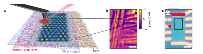
Our experimental workflow is schematically pictured in Fig. 1a. We fabricated a heterostructure consisting of hBN-encapsulated MATBG where the top encapsulating layer is closely aligned to the upper graphene layer as we verified with AFM measurements (Supplementary Note I). The heterostructure is contacted to a set of Cr/Au metallic leads (see Methods and Fig. 1c). In order to visualize the SOSL potential, defined here as electronic potential landscape governed by the atomic lattice structure, we employ a scattering-type scanning near-field imaging microscope operating at a temperature down to 10 K. By focusing infrared light (excitation energy meV, corresponding to wavelength m) to the apex of a sharp metal-coated AFM tip (radius of 20 nm), a hot-spot of light is generated that induces local photoexcitation of the charge carriers at the nanoscale. This leads to a local photovoltage generation that is probed by the global contacts, facilitated by the Shockley-Ramo mechanism 30 (see Fig. 1b,c). Details of the cryogenic near-field photovoltage measurements can be found in the Methods.
Photovoltage nanoscopy on a second-order superlattice The main experimental observation is shown in Fig. 1b, featuring a photovoltage map of our MATBG sample at K. Surprisingly, we observe photovoltage fringes that span across the entire bulk of the sample. In particular, in the top-left corner we observe a clear superposition of two sets of almost vertical and almost horizontal fringes (highlighted by the black circle).
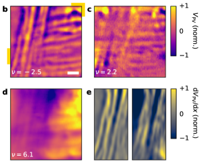
To further unravel the nature of the observed photovoltage periodicities, we map the photovoltage response for different gate voltages (Fig. 2a-d). We observe a very similar photovoltage pattern at charge neutrality (Fig. 2a) and with the Fermi level inside the moiré flat bands (Fig. 2b and c), as well as at a partial filling outside the flat band (Fig. 2d). In particular, the observed periodicity does not change with gate voltage. We also find that the photovoltage response is enhanced by an order of magnitude for fillings outside the flat band, with the features appearing to be less pronounced. (Fig. 2d). To accentuate that the underlying structure remains unchanged with filling factor, we show in Fig. 2e the spatial derivatives of the photovoltage response and we find a clear resemblance between the observed features at the Fermi levels inside and outside the flat band fillings. As a consequence, the observed features cannot be linked with electronic interactions, since the electron dynamics changes drastically between the charge densities inside and outside the flat band fillings, but rather originate from a modulating potential background.
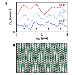
Additional evidence of a modulating potential background is further corroborated by photovoltage measurements as a function of temperature. Fig. 2f depicts normalized photovoltage line cuts and shows an unchanged response with temperature, aside from the magnitude (Supplementary Note II shows the full spatial photovoltage maps at different temperatures). This observation also suggests that the role of electronic interactions in creating the periodic photovoltage response remains irrelevant. From these line traces we extract a periodicity of the SOSL potential of nm, which falls within the resolution limit of our experiment (see Supplementary Note III).
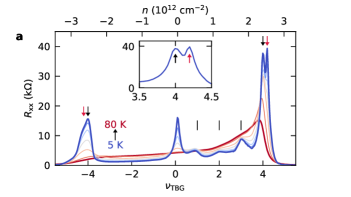
In order to confirm the presence of a SOSL and further characterize its properties, we explore its low-temperature electronic transport properties shown in Fig. 3a (see Methods for details). A set of transport curves vs. band filling taken at temperatures between 5 K and 80 K clearly indicates the presence of flat bands in our twisted bilayer graphene device. We identify characteristic local resistance maxima at integer fillings close to , +2, and +3 (marked by black lines), confirming the magic-angle nature of our device. In addition, we observe two pronounced band insulator resistance peaks characteristic for fully-filled or -emptied electronic flat bands at . Interestingly, instead of observing a single resistance peak, we observe split resistance maxima at and a shoulder at that appear nearly symmetric around the charge-neutrality point (CNP). Here we argue that this electronic transport signature originates from a close alignment between hBN and MATBG, which we further confirm by inspecting the AFM topography (Supplementary Note I) and extracting a large thermally-activated gap at CNP of meV Supplementary Note IV). The latter is a signature signalling the Dirac cones gap opening due to the graphene/hBN alignment31. Overall, we find that the lower density peak originates from a single-particle gap in MATBG (marked by the black arrow) and the higher density peak is a result of alignment between MATBG and hBN plane (marked by the red arrow) 32, 33.
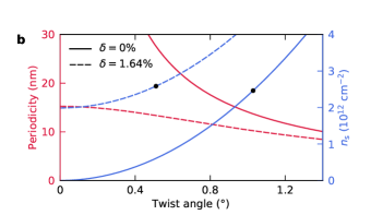
After carefully extracting the charge carrier density using the Hall effect, we define the twist angles (between hBN and bottom graphene) and (between the two graphene layers) based on the resistance peak positions (see Methods). Fig. 3b relates the charge carrier density expected at a fully filled moiré band in the case of twisted graphene layers (solid lines, lattice mismatch ) and in the case of graphene/hBN (dashed lines, lattice mismatch 2). Here, the black markers correspond to charge carrier densities extracted from Fig. 3a, from where we determine and . We note that our device shows a little twist angle variations of (Supplementary Note IV), in line with the presence of a SOSL across the entire sample, despite its high twist-angle sensitivity.


Electronic transport measurements strongly suggest that the sample hosts two coexisting superlattices. They are formed by a graphene layer closely aligned to hBN and the TBG superlattice, with periodicities of about 13.4 and 13.7 nm, respectively (deduced as in Fig. 3b). These two superlattices give rise to a SOSL with an even larger periodicity 34, 35, 36. Figure 1a shows an example of such second-order superlattice, mimicking the configuration in our sample. An hBN flake (green) has a small lattice mismatch and misalignment with respect to a graphene sheet (red), while a second graphene sheet has only a slight twist (blue).
Notably, our photovoltage maps provide a real-space image of the broken inversion symmetry in the MATBG superlattice. MATBG becomes asymmetric with respect to inversion when closely aligned to the adjacent hBN layer (Fig. 2g). Our observation of a complex real-space patterns of the second-order superlattice constitutes a first realization of inversion symmetry breaking imaged over the entire bulk of the studied device. Yet, we do not observe any signatures of the anomalous Hall effect (AHE) in electronic transport measurements. This is consistent with recent theoretical predictions and local magnetometry experiments where only very specific twist angles between TBG and hBN/graphene satisfy a commensurate condition for an AHE state 37, 38.
Calculation of spatial potential profile To model the spatial potential profile of the second-order superlattice, we examine its formation in the reciprocal space. In this work, we consider the case of an unstrained and strained heterostructure. First, we start with the case without applied strain. Figure 4a shows the lattice vectors of the unstrained hBN and graphene lattices, from which we take the difference vectors (blue) that represent their SOSL. These vectors feature a strongly reduced length and by taking the inverse of their moduli (and accounting for a factor ), we find the periodicity of the SOSL (also defined analytically in the Methods). Figure 4c depicts the SOSL periodicity for a range of and . We note that is equal in the three principal directions (representing a triangular lattice). We find a limited window of twist angles where a SOSL can be detected in our experiment, that is where . This is understood as in reciprocal space the superlattice vectors need to line up very closely with each other, while they also depend sensitively on hBN and graphene lattice mismatch , and . For and the twist angles extracted from the transport measurements, we find nm, which is slightly lower than the periodicity extracted in the near-field photovoltage maps. Note, it is a lucky coincidence that the hBN-graphene lattice mismatch happens to be such that SOSLs appear for twist angles near the magic angle.
We now move to the case where lattice strains become important actors in overall SOSL formation. Our minimalistic model of a triangular lattice lacks an explanation for the observation of periodic fringes in only two directions, which in turn are separated by an unexpected angle of (dashed lines in Fig.2a). To account for that, we introduce a small amount of a uniaxial heterostrain to the graphene layers, which is commonly present in these heterostructures 9, 39, 40, 41, 42. We apply a strain tensor to the graphene lattice vectors 43, 44, following , where
| (1) |
where is the angle of the principal direction of applied uniaxial strain with respect to the zigzag direction, and is the Poisson ratio of graphene 45. is the identity matrix. As illustrated in Fig. 4b, strain has a large impact on the relative magnitude and direction of the second-order superlattice vectors. This leads to a deformation of the lattice, such that superlattices act as ‘magnifying glasses’ of strain 46, 47. We repeat the calculation of with strain9, 39, 40, 41, 42 applied to both graphene layers along the zigzag direction (Supplementary Note V discusses details of these calculations in the presence of strain). The blue vectors in Fig. 4b become modified and now have three different moduli, which would naively be represented by three separate red color blobs in the - space.
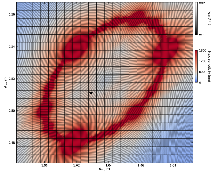
Figure 4d displays the maximum periodicity of three principal lattice vectors and reveals an intricate picture of strongly varying periodicities for different twist angles. Notably, this distribution is much more complex than expected from a simple picture introduced in Fig. 4a. Here, we take into account that a simple vector summation may end up with a set of lattice vectors representing by obtuse triangles. Since that would lead to an overestimation of we correct for it by remapping the lattice vectors until we reach an acute triangle, allowing for a fair comparison of with . This leads to the SOSL unit cell size that is represented by a fractal-like ring of non-vanishing wavelengths (Fig. 4d).
To obtain a better understanding of this result, we focus our attention to three particular sets of parameters (, , ) and visualize the real-space potential of the resulting second-order superlattice. As demonstrated in Fig. 4e, tiny variations in the twist angle and strain have a large impact on the type of second-order superlattice. For instance, by applying 0.1% of strain, the geometry may change from a triangular to a 1D lattice. Likewise, a square lattice can be formed by changing both twist angles only slightly. We calculate the real-space potential for a wider range of both twist angles, as presented in the birds-eye view in Figure 5. We emphasize that smaller periodicities must emerge in other non-dominant directions as well. However, these cannot be measured using our near-field probe with a limited spatial resolution and spatial selectivity of the global electrical photovotage probes. We can identify the following features: at three resonant points, a 1D lattice emerges with an even longer periodicity than our sample lateral dimensions, and hence is not detectable. Surrounding these points, 1D lattice structures are present with periodicities on the order of several hundreds of nanometers. Further away from these resonant points, the periodicity tends to fall below the experimental resolution and thus could not be observed. On the other hand, a triangular lattice forms right in the middle of these resonant points, which in turn converts via a square lattice towards a 1D lattice near those resonant points. This clearly illustrates the wide variety of lattices that can be formed in the limited parameter space of our experiment: (, , ).
PV generation mechanism How do we interpret the observed bulk photoresponse that does not decay away from contacts? Here, we assume that the periodicities (i.e. the spatial frequencies) embedded in the combined hBN/MATBG lattice structure are preserved in the lattice potential, and subsequently in the electronic properties that could induce a photovoltage. As we established above, there must be at least one non-linearity in the optoelectronic response pathway (Supplementary Note VI).
In many cases, the optoelectronic response in graphene-based devices is primarily facilitated by the photothermoelectric effect (PTE), which drives a photovoltage that is proportional to the spatial gradients in the Seebeck coefficient 48, 49, 50, 51, 30. Also in our case, it could play a role in the photoresponse pathway, since the Seebeck coefficient is a function of the electrical conductivity, which in turn is governed by the electronic properties of the atomic lattice. Hence, this pathway will provide a projection of the underlying lattice structure on the photovoltage maps. In this scenario, we can explain the strong enhancement of photovoltage response for higher filling factors (as seen in Fig 2d) by an increased cooling length due to the enhanced charge carrier mobility in the remote bands, as well as by the absorption efficiency and strength of the generating photovoltage mechanism 52. In the vicinity of more mobile charge carriers (i.e., outside the flat band regime), the photovoltage electrodes become less sensitive to spatial Seebeck coefficient variations, while the reduced charge carrier mobility inside the flat band boosts our probes’ spatial sensitivity.
Another possible PV generation mechanism is the second-order photoresponse, which has been reported to be more significant in flat band systems 53, 54, 55, 56, and this is enabled when inversion symmetry is broken by utilizing hBN alignment, as is seen in our system. Additionally, strain can lead to a non-zero bulk photoresponse for unpolarized light. Specifically, infrared inter-band transitions in twisted bilayer graphene were found to produce a dominant second-order photocurrent response (linear shift current). Generally, it is likely that bulk photovoltaic effects will take precedence at low temperatures, and it has been shown to lead to an increased magnitude for fillings above =4. However, we emphasize that comprehensive understanding of the photovoltage generation mechanism is not strictly required to explain the dataset shown in the current study and will remain the focus of the future reports.
Outlook To conclude, we have realized and observed a second-order superlattice formed by the alignment of MATBG to one of the adjacent hBN substrates. These observations, corroborated by our theoretical model, demonstrate a wide tuneability of the SOSL structures. In combination with controlled ways 57, 58 to tune , or strain , it will open the pathway to explore optoelectronic properties of a variety of different SOSL structures including triangular, square and 1D lattices. In particular, the latter holds a promise to explore Luttinger liquid states with a tuneable crystalline quality 1D channels59. The alignment of MATBG and hBN has been found to promote the emergence of unique quantum states displaying the quantum anomalous Hall effect60. Our study sheds a new light on the mesoscale precursors of such alignment. Some open questions, however, remain. For example, what exact mechanism drives the photovoltage in the SOSLs and what is at the cause of the required non-linear effect playing a significant role in the photovoltage generation? Further experiments are needed to reveal a mesoscopic picture of inversion symmetry breaking in moiré materials due to alignment with hBN and the role of strain profiles.
Methods
Device fabrication
The device consists of TBG encapsulated in 16 nm bottom hBN and 10 nm top hBN flakes, altogether placed on top of a graphite flake, serving as a local gate. During the stacking process, the graphene flake is cut with an AFM tip, with intention to prevent additional strain building up in the tear-and-stack process used otherwise 61, 62, 23. To minimize the number of bubbles in the stack, we pick up each flake at a temperature within C 63, 64. In the final step, when dropping the stack on the target substrate with alignment markers, we repeat the drop-down step at least once to further squeeze out air bubbles. Figure S1 shows an AFM scan of the resulting stack. We choose the cleanest area of the stack to pattern our device in a Hall-bar shape (Fig. 1c).
Cryogenic near-field photovoltage measurement details
We used a cryogenic scattering-type scanning near-field microscope (cryoSNOM) developed by Neaspec/Attocube to carry our the near-field photovoltage experiments at temperatures between K. A tuneable quantum cascade laser (Daylight Solutions) acts as an infrared light source, and the data shown in this work were acquired at an excitation energy of meV (10.6 m). We focus approximately 10 mW of this light on a PtIr-coated AFM tip (Nanoworld, 50 nm coating), which is oscillating above the sample surface at kHz with a tapping amplitude of nm. The AFM feedback loop incorporates a system developed by Neaspec/Attocube by which we can lower the quality factor of the AFM cantilever resonance to the values similar to ambient operation at room temperature. This helps a quick decay of the cantilever motion, and therefore we are less limited in the scanning speed. Finally, to reduce coupling of strong floor vibrations with our microscope, we set up a home-built active damping system that cancels these vibrations and stabilizes the optical table.
For simultaneous measurement of the photovoltage between two pairs of contacts, we used two differential voltage amplifiers (Ithaco 1201) with a different contact providing the ground. The carrier doping in our samples is tuned by applying a DC voltage between the graphite gate and our device, while keeping the Si backgate grounded. To avoid detecting unwanted far-field contributions to the photovoltage signal, we detect the near-field signals at the second harmonic of the cantilever oscillation.
We follow Ref. 51 in the scheme for analysing the photovoltage maps. Here, the measured photovoltage signal is demodulated with the driving signal of the AFM cantilever as a reference signal. However, the actual motion of the AFM cantilever can have a phase offset that varies with the position on the sample (due to tip–sample interaction). This phase offset is given at each pixel by the measured phase delay between the tip driving signal and the actually detected motion. Therefore, we correct our photovoltage signal measured at harmonic by subtracting at every point times this phase delay. In addition to this, there remains a global phase offset in the corrected photovoltage signal due to the electronics in the circuit. Since the photovoltage signal is a real-valued quantity, we subtract this global phase offset, which we determine by taking the most frequent phase within a scan.
Transport measurement details
The main set of four-terminal transport data shown in Fig. 3a was taken in an Advanced Research System cryostat with base temperature of 5 K and magnetic field up to 1 T. In these electronic transport measurements we followed a conventional lock-in measurement scheme. A low-frequency AC current (17.111 Hz) of 10 nA flows between the bottom-right and top contacts, while measuring the voltage drop between the two left-middle contacts using a Stanford SR860 lock-in amplifier. The gate voltage was sourced using a Keithley 2400 Source Meter Unit.
Analysis of transport data
From a Hall measurement in a magnetic field of 1 T we determine the carrier density (in ) as a function of the applied gate voltage . A linear fit near the charge-neutrality points ( V) yields in units of . For the subsequent analysis we allow for a small shift in the charge neutrality voltage (for instance induced by photodoping 65) by replacing with . From the peak value of the resistance peak at charge neutrality in Fig. 3a we find mV. We define the full-filling carrier density as half the distance from the two resistance peaks marked by the black arrows in Fig. 3a. In this, we notice that these two peaks are slightly off-centered with respect to the charge neutrality by 60 mV. The resistance peak of the hBN-Gr superlattice is less developed for negative carrier densities. Therefore we extract the corresponding to the hBN-Gr lattice from the relative scaling of the Gr-Gr and hBN-Gr superlattice peaks at positive carrier densities (marked in black and red, respectively).
First-order superlattice periodicity
Our transport data reveals two moiré lattices hosted by our sample: one given by graphene aligned to hBN, and another one owing to twisted bilayer graphene (TBG). Such moiré lattices exhibit a resistive state at a particular carrier density associated with the full-fulling state of the superlattice 33, 66. For a superlattice formed by two superposed hexagonal lattices, this full-filling carrier density is given by 33
| (2) |
where the twist angle and lattice mismatch define the superlattice periodicity as
| (3) |
with nm corresponding to the graphene lattice periodicity. The properties of TBG are reflected by the curves with , while we model hBN-graphene superlattice with . This value is slightly lower than the value typically stated in literature, , However, the typical amount of strain in the graphene layers of can account for this difference.
References
- [1] Cao, Y. et al. Unconventional superconductivity in magic-angle graphene superlattices. Nature 556, 43–50 (2018).
- [2] Cao, Y. et al. Correlated insulator behaviour at half-filling in magic-angle graphene superlattices. Nature 556, 80–84 (2018).
- [3] Yankowitz, M. et al. Tuning superconductivity in twisted bilayer graphene. Science 363, 1059–1064 (2019).
- [4] Lu, X. et al. Superconductors, orbital magnets and correlated states in magic-angle bilayer graphene. Nature 574, 653–657 (2019).
- [5] Zondiner, U. et al. Cascade of phase transitions and Dirac revivals in magic-angle graphene. Nature 582, 203–208 (2020).
- [6] Xie, M. & MacDonald, A. H. Nature of the Correlated Insulator States in Twisted Bilayer Graphene. Physical Review Letters 124, 097601 (2020).
- [7] Po, H. C., Zou, L., Vishwanath, A. & Senthil, T. Origin of mott insulating behavior and superconductivity in twisted bilayer graphene. Physical Review X 8, 031089 (2018).
- [8] Dodaro, J. F., Kivelson, S. A., Schattner, Y., Sun, X.-Q. & Wang, C. Phases of a phenomenological model of twisted bilayer graphene. Physical Review B 98, 075154 (2018).
- [9] Wong, D. et al. Cascade of electronic transitions in magic-angle twisted bilayer graphene. Nature 582, 198–202 (2020).
- [10] Xie, F., Song, Z., Lian, B. & Bernevig, B. A. Topology-bounded superfluid weight in twisted bilayer graphene. Physical review letters 124, 167002 (2020).
- [11] Balents, L., Dean, C. R., Efetov, D. K. & Young, A. F. Superconductivity and strong correlations in moiré flat bands. Nature Physics 16, 725–733 (2020).
- [12] Lian, B., Wang, Z. & Bernevig, B. A. Twisted bilayer graphene: a phonon-driven superconductor. Physical review letters 122, 257002 (2019).
- [13] Gonzalez, J. & Stauber, T. Kohn-luttinger superconductivity in twisted bilayer graphene. Physical review letters 122, 026801 (2019).
- [14] Isobe, H., Yuan, N. F. & Fu, L. Unconventional superconductivity and density waves in twisted bilayer graphene. Physical Review X 8, 041041 (2018).
- [15] Liu, C.-C., Zhang, L.-D., Chen, W.-Q. & Yang, F. Chiral spin density wave and d+ i d superconductivity in the magic-angle-twisted bilayer graphene. Physical review letters 121, 217001 (2018).
- [16] Bistritzer, R. & MacDonald, A. H. Moiré bands in twisted double-layer graphene. Proceedings of the National Academy of Sciences 108, 12233–12237 (2011).
- [17] Koshino, M. et al. Maximally localized wannier orbitals and the extended hubbard model for twisted bilayer graphene. Physical Review X 8, 031087 (2018).
- [18] Kang, J. & Vafek, O. Strong coupling phases of partially filled twisted bilayer graphene narrow bands. Physical review letters 122, 246401 (2019).
- [19] Nuckolls, K. P. et al. Strongly correlated chern insulators in magic-angle twisted bilayer graphene. Nature 588, 610–615 (2020).
- [20] Wu, S., Zhang, Z., Watanabe, K., Taniguchi, T. & Andrei, E. Y. Chern insulators, van hove singularities and topological flat bands in magic-angle twisted bilayer graphene. Nature materials 20, 488–494 (2021).
- [21] Saito, Y. et al. Hofstadter subband ferromagnetism and symmetry-broken chern insulators in twisted bilayer graphene. Nature Physics 17, 478–481 (2021).
- [22] Saito, Y. et al. Isospin pomeranchuk effect in twisted bilayer graphene. Nature 592, 220–224 (2021).
- [23] Stepanov, P. et al. Untying the insulating and superconducting orders in magic-angle graphene. Nature 583, 375–378 (2020).
- [24] Arora, H. S. et al. Superconductivity in metallic twisted bilayer graphene stabilized by WSe2. Nature 583, 379–384 (2020).
- [25] Serlin, M. et al. Intrinsic quantized anomalous Hall effect in a moiré heterostructure. Science 367, 900–903 (2020).
- [26] Sharpe, A. L. et al. Emergent ferromagnetism near three-quarters filling in twisted bilayer graphene. Science 365, 605–608 (2019).
- [27] Oh, M. et al. Evidence for unconventional superconductivity in twisted bilayer graphene. Nature 600, 240–245 (2021).
- [28] Wagner, G., Kwan, Y. H., Bultinck, N., Simon, S. H. & Parameswaran, S. Global phase diagram of the normal state of twisted bilayer graphene. Physical Review Letters 128, 156401 (2022).
- [29] Jiang, Y. et al. Charge order and broken rotational symmetry in magic-angle twisted bilayer graphene. Nature 573, 91–95 (2019).
- [30] Ma, Q., Kumar, R. K., Xu, S.-Y., Koppens, F. H. L. & Song, J. C. W. Photocurrent as a multi-physics diagnostic of quantum materials (2022).
- [31] Zhang, Y.-H., Mao, D. & Senthil, T. Twisted bilayer graphene aligned with hexagonal boron nitride: Anomalous Hall effect and a lattice model. Physical Review Research 1, 033126 (2019).
- [32] Dean, C. R. et al. Hofstadter’s butterfly and the fractal quantum Hall effect in moiré superlattices. Nature 497, 598–602 (2013).
- [33] Yankowitz, M. et al. Emergence of superlattice Dirac points in graphene on hexagonal boron nitride. Nature Physics 8, 382–386 (2012).
- [34] Wang, L. et al. New Generation of Moiré Superlattices in Doubly Aligned hBN/Graphene/hBN Heterostructures. Nano Letters 19, 2371–2376 (2019).
- [35] Finney, N. R. et al. Tunable crystal symmetry in graphene–boron nitride heterostructures with coexisting moiré superlattices. Nature Nanotechnology 14, 1029–1034 (2019).
- [36] Wang, Z. et al. Composite super-moiré lattices in double-aligned graphene heterostructures. Science Advances 5, eaay8897 (2019).
- [37] Shi, J., Zhu, J. & MacDonald, A. Moiré commensurability and the quantum anomalous hall effect in twisted bilayer graphene on hexagonal boron nitride. Physical Review B 103, 075122 (2021).
- [38] Grover, S. et al. Chern mosaic and berry-curvature magnetism in magic-angle graphene. Nature Physics 1–8 (2022).
- [39] Jiang, L., Wang, S., Zhao, S., Crommie, M. & Wang, F. Soliton-Dependent Electronic Transport across Bilayer Graphene Domain Wall. Nano Letters 20, 5936–5942 (2020).
- [40] Benschop, T. et al. Measuring local moiré lattice heterogeneity of twisted bilayer graphene. Physical Review Research 3, 013153 (2021).
- [41] Kazmierczak, N. P. et al. Strain fields in twisted bilayer graphene. Nature Materials 20, 956–963 (2021).
- [42] Mesple, F. et al. Heterostrain rules the flat-bands in magic-angle twisted graphene layers. arXiv:2012.02475 (2020).
- [43] Pereira, V. M., Castro Neto, A. H. & Peres, N. M. R. Tight-binding approach to uniaxial strain in graphene. Physical Review B 80, 045401 (2009).
- [44] Naumis, G. G., Barraza-Lopez, S., Oliva-Leyva, M. & Terrones, H. Electronic and optical properties of strained graphene and other strained 2D materials: a review. Reports on Progress in Physics 80, 096501 (2017).
- [45] Blakslee, O. L., Proctor, D. G., Seldin, E. J., Spence, G. B. & Weng, T. Elastic Constants of Compression-Annealed Pyrolytic Graphite. Journal of Applied Physics 41, 3373–3382 (1970).
- [46] Cosma, D. A., Wallbank, J. R., Cheianov, V. & Fal’ko, V. I. Moiré pattern as a magnifying glass for strain and dislocations in van der Waals heterostructures. Faraday Discuss. 173, 137–143 (2014).
- [47] Jiang, Y. et al. Visualizing Strain-Induced Pseudomagnetic Fields in Graphene through an hBN Magnifying Glass. Nano Letters 17, 2839–2843 (2017).
- [48] Gabor, N. M. et al. Hot Carrier-Assisted Intrinsic Photoresponse in Graphene. Science 334, 648–652 (2011).
- [49] Lemme, M. C. et al. Gate-Activated Photoresponse in a Graphene p–n Junction. Nano Letters 11, 4134–4137 (2011).
- [50] Woessner, A. et al. Near-field photocurrent nanoscopy on bare and encapsulated graphene. Nature Communications 7, 10783 (2016).
- [51] Hesp, N. C. H. et al. Nano-imaging photoresponse in a moiré unit cell of minimally twisted bilayer graphene. Nature Communications 12, 1640 (2021).
- [52] Deng, B. et al. Strong mid-infrared photoresponse in small-twist-angle bilayer graphene. Nature Photonics 14, 549–553 (2020).
- [53] Chaudhary, S., Lewandowski, C. & Refael, G. Shift-current response as a probe of quantum geometry and electron-electron interactions in twisted bilayer graphene. Physical Review Research 4, 013164 (2022).
- [54] Ma, C. et al. Intelligent infrared sensing enabled by tunable moiré quantum geometry. Nature 604, 266–272 (2022).
- [55] Arora, A., Kong, J. F. & Song, J. C. Strain-induced large injection current in twisted bilayer graphene. Physical Review B 104, L241404 (2021).
- [56] Kaplan, D., Holder, T. & Yan, B. Twisted photovoltaics at terahertz frequencies from momentum shift current. Physical Review Research 4, 013209 (2022).
- [57] Ribeiro-Palau, R. et al. Twistable electronics with dynamically rotatable heterostructures. Science 361, 690–693 (2018).
- [58] Inbar, A. et al. The quantum twisting microscope. arXiv preprint arXiv:2208.05492 (2022).
- [59] Wang, P. et al. One-dimensional luttinger liquids in a two-dimensional moiré lattice. Nature 605, 57–62 (2022).
- [60] Tschirhart, C. L. et al. Imaging orbital ferromagnetism in a moiré chern insulator. Science 372, 1323–1327 (2021).
- [61] Chen, G. et al. Evidence of a gate-tunable Mott insulator in a trilayer graphene moiré superlattice. Nature Physics 15, 237–241 (2019).
- [62] Saito, Y., Ge, J., Watanabe, K., Taniguchi, T. & Young, A. F. Independent superconductors and correlated insulators in twisted bilayer graphene. Nature Physics 16, 926–930 (2020).
- [63] Pizzocchero, F. et al. The hot pick-up technique for batch assembly of van der Waals heterostructures. Nature Communications 7, 11894 (2016).
- [64] Purdie, D. G. et al. Cleaning interfaces in layered materials heterostructures. Nature Communications 9, 5387 (2018).
- [65] Ju, L. et al. Photoinduced doping in heterostructures of graphene and boron nitride. Nature Nanotechnology 9, 348–352 (2014).
- [66] Cao, Y. et al. Superlattice-Induced Insulating States and Valley-Protected Orbits in Twisted Bilayer Graphene. Physical Review Letters 117, 116804 (2016).
Acknowledgements
F.H.L.K. acknowledges financial support from the Government of Catalonia trough the SGR grant, and from the Spanish Ministry of Economy and Competitiveness, through the Severo Ochoa Programme for Centres of Excellence in R&D (Ref. SEV-2015-0522), and Explora Ciencia (Ref. FIS2017-91599-EXP). F.H.L.K. also acknowledges support by Fundacio Cellex Barcelona, Generalitat de Catalunya through the CERCA program, and the Mineco grant Plan Nacional (Ref. FIS2016-81044-P) and the Agency for Management of University and Research Grants (AGAUR) (Ref. 2017-SGR-1656). Furthermore, the research leading to these results has received funding from the European Union’s Horizon 2020 programme under grant agreements Refs. 785219 (Graphene Flagship Core2) and 881603 (Graphene Flagship Core3), and Ref. 820378 (Quantum Flagship). This work was supported by the ERC under grant agreement Ref. 726001 (TOPONANOP). P.S. acknowledges support from the European Union’s Horizon 2020 research and innovation programme under the Marie Skłodowska-Curie Grant No. 754510. N.C.H.H. acknowledges funding from the European Union’s Horizon 2020 research and innovation programme under the Marie Skłodowska-Curie grant agreement Ref. 665884. K.W. and T.T. acknowledge support from JSPS KAKENHI (Grant Refs. 19H05790, 20H00354 and 21H05233). This project has received funding from the “Presidencia de la Agencia Estatal de Investigación” within the PRE2020-094404 predoctoral fellowship.
Author contributions
F.H.L.K. conceived the experiment. N.C.H.H., S.B.-P., P.S. performed near-field experiments on a system optimized by N.C.H.H., D.B.-R. and H.H.S. Transport experiments were performed by P.S. on a system built by R.K.K. The sample was fabricated by P.S. using a contact recipe developed by H.A. and with hBN crystals provided by K.W. and T.T. The results were analyzed and interpreted by N.C.H.H. and P.S. using a model developed by N.C.H.H. The manuscript was written by P.S., N.C.H.H. and F.H.L.K. with input from all authors. F.H.L.K supervised the work.
Competing Financial Interests
The authors declare no competing financial interests.
Data Availability Statement
The data that support the plots within this paper and other findings of this study are available from the corresponding authors upon reasonable request.