On-chip time-domain terahertz spectroscopy of superconducting films below the diffraction limit
Abstract
Free-space time domain THz spectroscopy accesses electrodynamic responses in a frequency regime ideally matched to interacting condensed matter systems. However, THz spectroscopy is challenging when samples are physically smaller than the diffraction limit of 0.5 mm, as is typical, for example, in van der Waals materials and heterostructures. Here, we present an on-chip, time-domain THz spectrometer based on semiconducting photoconductive switches with a bandwidth of 200 GHz to 750 GHz. We measure the optical conductivity of a 7.5-um wide NbN film across the superconducting transition, demonstrating spectroscopic signatures of the superconducting gap in a sample smaller than 2% of the Rayleigh diffraction limit. Our spectrometer features an interchangeable sample architecture, making it ideal for probing superconductivity, magnetism, and charge order in strongly correlated van der Waals materials.
Terahertz time-domain spectroscopy (THz TDS) can be used to extract the complex optical conductivity of quantum materials without Kramers-Kronig relations. The few-meV energy scale and the picosecond time scale of a typical THz pulse makes THz spectroscopy well suited to experiments in many fields of research, particularly strongly correlated phenomena [1, 2, 3, 4], superconductivity [5, 6, 7, 8] and non-equilibrium dynamics[6, 9]. However, free space THz TDS, which has been used extensively to study bulk materials and thin films, cannot be used directly to study correlated phenomena in van der Waals heterostructures, an increasingly active area for probing these same phenomena [10, 11, 12]. Free space THz TDS inherently suffers from the inability to focus THz beams on samples smaller than the Rayleigh diffraction limit of 488 m at 0.75 THz. vdW heterostructures, often m or smaller, have a reduced cross-section with free-space THz beams, leading to a drastically diminished signal-to-noise ratio that precludes most experiments. Though THz near-field imaging techniques [13, 14, 15, 16, 17, 18] can achieve extreme sub-wavelength resolution, they are often difficult to integrate into cryostats, have low excitation efficiency if standard far-field excitation techniques are used, and are limited to narrow bands of THz frequencies.
The diffraction limit can also be circumvented by confining THz pulses within transmission lines patterned on a chip. Early on-chip THz experiments incorporated photoconductive (PC) switches into transmission line circuits to emit and detect THz radiation[19, 20, 21]. Recent on-chip THz efforts[22, 23, 24, 25, 26, 27, 28, 29, 30, 31] have explored new geometries, leading to increases in the THz amplitude and spectral bandwidth. On-chip THz TDS has been recently used to study electronic phases at cryogenic temperatures in carbon nanotubes [32], topological insulators [4], and two-dimensional electronic systems such as GaAs [33] and graphene [34, 35, 36, 37, 38]. Most of the existing designs for on-chip THz spectroscopy require monolithic fabrication of the THz emitter/receiver and the vdW device. The combined complexity of fabricating both the THz spectrometer and a vdW device to perform a single experiment, however, reduces measurement throughput.
Higher throughput may be achieved by disentangling the fabrication of the THz spectrometer (switch board) and the device (on the sample board) as introduced recently by Lee et al. [39] at room temperature. Here, we demonstrate cryogenic operation of an on-chip THz spectrometer with a fast sample exchange architecture, and use it to extract the complex optical conductivity of a lithographically-defined NbN device below its superconducting transition temperature. Our experimental geometry is shown in Fig.1, and consists of a ‘switch board’ containing transmission lines and photoconductive switches for both THz generation and readout and an interchangeable ‘sample board’ containing a sample of interest, transmission line segments, and additional deposited electrical contacts.
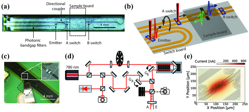
The switch board is a permanent fixture containing low temperature (LT) grown GaAs PC switches coupled to lithographically defined coplanar stripline transmission lines (Fig.1a). The transmission lines have a conductor width of m, a separation of m, and are terminated by photonic bandgap filters that reduce THz reflections from the transmission line terminations at long times. The switch board is fabricated on a m thick cyclo-olefin polymer (COP) substrate. High transparency, low permeability and a nearly temperature and frequency-independent optical index of 1.52 at THz frequencies ensures minimal pulse broadening [40, 41, 42]. The thin substrate and comparatively small dielectric constant substrate mitigates the -dependent Cerenkov radiation loss that often dominates on-chip THz propagation [43, 44, 45, 46, 28, 21]. In addition, the local dielectric environment of thin COP substrates does not support unbound leaky-wave modes (see supplementary).
We use separate transmission lines for THz emission and detection. The transmission line for the THz detection is gapped between the detector A-switch and B-switch to allow for the placement of the sample board. Sample boards are fabricated on 50 m thick z-cut dual-side polished quartz. Nanofabrication of fragile 50 m quartz is accomplished by crystal-bonding quartz to a silicon carrier wafer, patterning the coplanar stripline (CPS) and performing any additional sample-related nanofabrication steps, and then dissolving the crystal bond to release the quartz film. The sample board is then aligned to the switch board under an optical microscope, resulting in a reliable placement precision of 10 m. The resulting combined structure is shown schematically in Fig.1b while a micrograph of an aligned thru sample board is shown in Fig.1c.
We illuminate both the emitter and detector (A/B) PC switches with 3 mW of 780 nm, 75 fs Gaussian laser pulses with a repetition rate of 250 MHz. The optical path is illustrated in Fig.1d. The beam to the emitter switch is chopped at 3.2 kHz, routed through an optical delay stage, directed on the emitter switch using a scanning galvanometer (GE), and focused to diameter . A beam-splitter extracts 500 W for power and spot stability monitoring on the A-switch beam path. We apply a 10V DC bias across the emitter switch, providing the energy that is converted into a THz transient in the emission line when the emitter switch is illuminated. This THz pulse is subsequently coupled to the detection transmission line via an inductive directional coupler, which provides a DC block between the emission and detection transmission lines (Fig.1b). To improve the stability of our measurements, we spatially map the DC photocurrent across the emitter switch using scanning galvanometer GE (Fig.1e), allowing us to stabilize switch operation at the position of maximum photocurrent through real-time feedback.
The beam for the detector switch is routed through another scanning galvanometer (GA) prior to being focused on the switch, thus allowing for automatic and precise alignment of the laser beam on the PC switches. The THz pulse traveling along the detection transmission line is then measured at the detector A-switch. The detector switch is momentarily triggered by an optical pulse and thus allows us to measure the current across the detector switch, which samples the local electric field across the detection PC switch. Since the instantaneous current across the detector A-switch is only hundreds of picoamps, we use a transimpedance amplifier with gain 1e-7 A/V, the output of which is then demodulated using a lock-in amplifier synchronized to the chopper. Sweeping the optical delay stage continuously allows us to vary the time delay of the optical pulses exciting the emitter and the detector switches. This allows us to extract the time-domain electric field of the incident, reflected, and transmitted THz pulse from the transients recorded at the PC switch A and B. We move the optical delay stage continuously, measuring the time-domain THz signal with a Nyquist frequency of nearly 350 THz. We, then, apply standard THz TDS signal processing [47, 48] and smooth the time-domain data with a 101-point, 3rd order Savitsky-Golay filter.
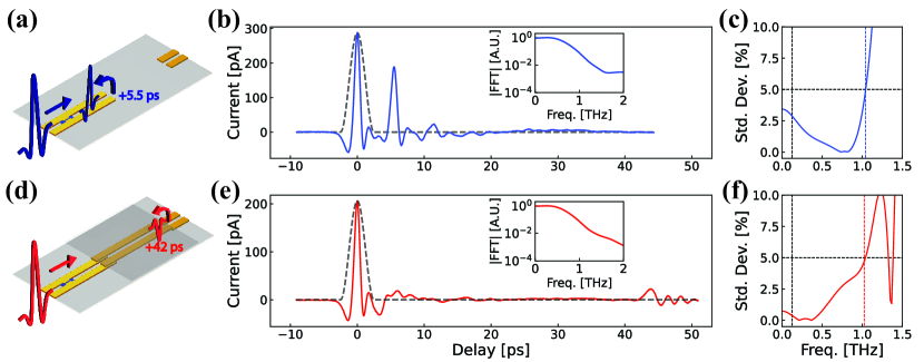
Fig. 2a-c show characterization data of the spectrometer at room temperature with no sample board mounted. In this configuration, the THz pulse traverses the A-switch (producing a ‘directivity’ peak at zero delay) and is subsequently reflected at the open termination of the transmission line, producing a peak 5.5 ps after the directivity. The directivity and reflected signal have the same polarity, correctly indicating that the transmission line termination behaves as an open circuit. Additional structure, including a weaker peak at 11 ps, results from Fabry-Perot reflections between the open circuit and A-switch. The spectral amplitude and phase of both the directivity pulse D() and the sample-reflected pulse R() are isolated using appropriate Hann windows and computed by Fourier transform. We define usable bandwidth as frequencies for which the standard deviation is less than 5% of the signal amplitude as shown in Fig. 2c, yielding a bandwidth of about 1 THz.
Characterization data for a sample board containing a bare transmission line (thru) are shown Fig. 2d-f. Accurate alignment of the transmission line allows the strength of the THz pulse reflected from the sample board interface (around 5.5ps) to be smaller than % of the directivity, indicating good coupling between switch and sample boards. The transmitted THz pulse propagates across the sample board transmission line until the second interface, where it undergoes another partial reflection. This reflected pulse is observed at the A-switch about 42 ps after the directivity. The reflected signal is featureless between 20 and 42 ps. This window corresponds to a significant fraction of the transmission line length on the sample board, and sets the bounds for placement of the device to be tested.
For both configurations, is reproducible to within 5% out to 1 THz (Fig. 2c and f). Recording and from the sample board interface (in addition to reflections from the device to be tested) allows us to characterize the emitted THz pulse and the sample board alignment. We consequently focus on THz reflection rather than transmission in what follows, even though our circuit permits the measurement of both THz reflection and transmission.
Having characterized the on-chip THz spectrometer at room temperature, we now demonstrate its cryogenic capability by extracting the complex optical conductivity () of a superconductor as it is cooled below its transition temperature. Conventional superconductivity exhibits distinct features such as the superconducting gap () in the real optical conductivity () and like response in the imaginary optical conductivity () [49]. To inform the design of the sample, we model a sample on the transmission lines as complex admittance connecting one metal line to the other. The admittance takes the form Y() = Y1() + jY2() for radial frequency and imaginary unit .The reflected signal R(YZ0,) is proportional to the directivity D() and sample reflection coefficient , which is given by:
| (1) |
where is the characteristic impedance of the transmission line. We are interested in maximizing the response to small changes in sample admittance , which can be expressed as . Using (1) for , we find that this quantity is maximized when YZ0 = 2. The lateral width and thickness of the superconducting film are thus chosen to satisfy the maximal contrast condition at temperatures just above the superconducting transition.
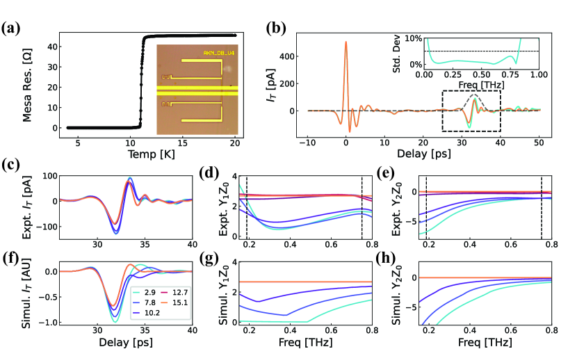
For the superconducting film, we use NbN, chosen for its moderate superconducting transition temperature (TC) and well-documented electrodynamics[50, 51, 52, 53, 54]. NbN films were deposited by magnetron sputtering (AJA ATC 2200-V sputtering system) with power 300W, pressure 1.8 mTorr, and 45/3.8 sccm Ar/N2 gas flow. The four-terminal DC transport curve is shown in 3a, with the data scaled by a geometric factor to accurately represent the resistance shorting the transmission line. The sample has a TC of 11.1K, where the TC is defined as 90% of the normal state resistance at 15K. With lateral width 7.5 m, the sample is 3.2% of one wavelength at 750 GHz, justifying the lumped element approximation. The sample thickness of 151 nm is chosen to bring the resistance in the normal state as close as possible to the maximum contrast condition. Experimentally, we find that the sample presented here has Y = 2.58 at room temperature, which, given the residual resistivity ratio of 0.94 for NbN, ensures good matching at low temperatures. The sample board containing the NbN film is aligned to the switch board and cooled down to 3K in an exchange gas environment. The exchange gas ensures thermalization of the sample, despite the poor thermal conductivity of the COP switch board.
To extract the complex admittance of the superconducting state, we assume a frequency-independent admittance in the normal state, , which we take to be equivalent to the conductance measured by DC transport. The ratio of the reflected signal in the normal and superconducting states can then be used to extract the superconductor’s admittance YS() via the relation:
| (2) |
The THz time-domain reflection signal of the NbN sample measured above and below the TC is presented in Fig. 3b, with the dashed box outline highlighting the signal reflected from the NbN device. The repeatability of the THz signal reflected from the sample at a temperature of 3K is shown in the inset, showing a usable bandwidth extending to GHz. The dynamic range, defined as the ratio of the peak Fourier amplitude and the background noise level exceeds 2000 for the NbN reflection.
Fig. 3c shows the time-domain reflection from the NbN, after application of the window shown in gray in Fig. 3b. The measured reflection is temperature independent at high temperatures but exhibits strong temperature dependence after the onset of superconductivity; qualitatively, the peak signal increases while simultaneously also shifting to later times by fs as the temperature is lowered below . These behaviors are consistent with expectations. Specifically, the increase in the peak reflection signal results from decreased THz absorption by normal carriers, while the lagging phase arises from the inductive response of the incipient Cooper pairs[55].
The real () and imaginary () admittance, expressed in units of transmission line impedance (), are extracted using Eq. 2 and are shown in Fig. 3d and e, respectively. Free space THz conductivity measurements of NbN in the normal state report a featureless real conductivity equal to the measured DC value and a negligible imaginary conductivity [50, 52] from DC to 750 GHz. We therefore use the DC value of YN for all measurable frequencies.
The upper and the lower frequency cutoffs are delineated with black dashed lines in Fig. 3d and e. The upper frequency cutoff is defined as the frequency at which the normalized standard deviation of the THz signal magnitude is at least 5% (inset), while the lower frequency cutoff is defined as the product of the minimum resolvable frequency of the windowed directivity or windowed NbN reflection and the equivalent noise bandwidth (ENBW) of the isolating Hann window of 1.5. The minimum resolvable frequency is given by the maximum size of the isolating window used for the reflection, which is set by the distance between the signal of interest and features arising from unwanted reflections such as those that occur at the switch board/sample board interface. Practically, in our current geometry the low frequency limit is 200 GHz. This could be be extended by increasing the physical spacing between the detector switch A and the switch-sample board interface.
We simulate the electromagnetic response of the superconductor using a model developed for disordered superconductors by Zimmerman and collaborators[49]. We take the NbN to be in impure limit (), use K, and use a superconducting gap of the following form:
| (3) |
where, is 500 GHz and is the Boltzmann constant. The simulated time-domain response of the superconductor and the corresponding real and imaginary admittances are plotted in Fig. 3f, g, and h, respectively. We use the complex admittance obtained from the BCS model[49] to simulate the reflected signal in the frequency domain, as shown in Fig. 3g and h. The time domain signal shown in Fig. 3f was then reconstructed from the complex admittance using the inverse Fourier transform.
The measured and the simulated time-domain profiles show similar qualitative features such as the increase in signal peak value and the phase lag below the superconducting transition temperature. The real admittance () of the superconducting state reduces as we go from the high frequency () response of the normal carriers into the gap (), followed by an increase due to thermal broadening of the superfluid peak at . The imaginary admittance () of the superconducting state shows the characteristic -like response indicative of the superfluid density, whose spectral weight increases as the temperature decreases.
While our results demonstrate the qualitative electrodynamic response of a superconducting thin film, further improvements in phase accuracy and bandwidth are needed to get a better quantitative understanding of, say, unconventional superconductors. Imperfect alignment of the laser spot and the PC switches, for instance, introduces a random variation in the THz emission and the propagation length of the THz pulses. We use the directivity ratio in Eq. 2 to calibrate the system, however, the THz path error of length subsequently accumulates to a phase error of . Better phase sensitivity can likely be achieved by miniaturizing the photoconductive switches to match the laser spot.
In summary, we have demonstrated a cryogenic-compatible on-chip THz spectrometer with a fast sample interchange architecture, and used it to extract the complex optical admittance of a deeply sub-wavelength superconducting NbN sample between 200 and 750 GHz. The confinement of the THz field within the transmission line and ease of sample interchange makes this spectrometer architecture ideal to investigate gate-tunable van der Waals heterostructures, with near-term applications to the physics of correlated electronic states and ultra-high frequency devices.
Acknowledgements.
The authors acknowledge discussions with V. Ramaprasad, L.A. Cohen, and B. Potts, and the assistance of P. Kissin in designing the optical set up. The early stages of this work (through mid-2022) were supported by the Army Research Office under No. MURI W911NF-16-1-0361. Work from 2022 until publication was supported by the National Science Foundation (NSF) Materials Research Science and Engineering Center (MRSEC) at UC Santa Barbara, Award DMR 1720256, through a seed grant and through the use of the MRL Shared experimental facilities. This work was additionally supported by the Gordon and Betty Moore Foundation EPIQS program under award GBMF9471. A portion of this work was performed in the UCSB Nanofabrication Facility, an open access laboratory. A portion of this work was performed at the Institute for Terahertz Science and Technology (ITST) at UCSB.Appendix A COP and unbound substrate modes
The generation of unbound leaky wave modes[56] greatly affects the ability of an on-chip THz spectrometer to measure the reflection and transmission from the device. Ideally, the THz pulse would propagate in only the CPS’s bound quasi-TEM mode [35]. If any coplanar transmission line and substrate dielectric environment supports leaky-wave modes, such modes are radiated isotropically upon emitter excitation. Some radiation goes into free space, some radiation is coupled to the transmission line as a bound mode, and some radiation is coupled as a leaky-wave mode in the substrate. All three types of modes are propagating THz electric fields that can be sampled by readout PC switches[57]. Unbound free space modes will propagate to the readout PC switch many picoseconds before the bound transient. The bound transmission line mode, then the unbound substrate modes, will reach the readout PC switch. Unbound substrate modes may propagate longitudinally in the substrate or may reflect from the substrate underside and edges, delaying their arrival at the readout PC switch by up to hundreds of picoseconds. As the substrate thickness is reduced, the substrate begins acting as a dielectric waveguide for unbound modes, producing measurable electric fields at long time delays.
To demonstrate the effects of unbound leaky-wave modes, a thru circuit was fabricated with two LT GaAs switches placed 10 mm apart (Fig. 4a). The emitter is connected to the thru CPS of the same dimensions used in the main text via an capacitive coupler. The circuit was fabricated on three substrates: 50 m thick COP, 180 m thick polyethylene terephthalate (PET) and 100 m thick sapphire. The resulting transients and their normalized Fourier transforms are shown in Fig. 4b-g.
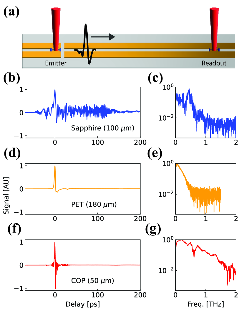
The measured transmission with a sapphire substrate shows a signal 35 ps before the main transient from unbound free space modes. The bound transient, mixed with unbound modes, appears at zero delay. Strong oscillations continue for 130 ps, due to the leaky wave substrate modes and their reflections from the substrate underside and periphery. After 130 ps, the oscillations reduce in amplitude, but do not vanish. The bound transient cannot be isolated with a narrow window because that peak contains bound and unbound contributions. Even if the bound transient could be isolated, the window would have to be so narrow that the minimum resolvable frequency would be reduced to about 1 THz.
The unbound mode cannot propagate for thin PET and COP substrates as a result of decreased substrate permittivity. The moderate loss tangent and dispersive index in PET, however, results in a bound transient with only 300 GHz bandwidth. COP’s frequency-independent index and minimal loss tangent result in a large signal, large bandwidth transient, even after 10 mm of propagation. COP is therefore the best of the three thin substrates for THz applications.
In the case of short ( mm) transmission lines fabricated on thick ( mm) substrates, the reflected leaky-wave modes do not have sufficient time to propagate to the readout PC switch and are thus not conflated with the desirable bound mode signal. Both short transmission lines and thick substrates are undesirable. Short transmission lines increase the minimum resolvable frequency; thick substrates suffer exacerbated Cerenkov radiation loss. The use of COP substrates mitigates both factors, although at a cost in difficulty of switch fabrication.
References
- Basov et al. [2011] D. N. Basov, R. D. Averitt, D. V. D. Marel, M. Dressel, and K. Haule, Electrodynamics of correlated electron materials, Reviews of Modern Physics 83, 471 (2011).
- Aguilar et al. [2012] R. V. Aguilar, A. V. Stier, W. Liu, L. S. Bilbro, D. K. George, N. Bansal, L. Wu, J. Cerne, A. G. Markelz, S. Oh, and N. P. Armitage, Terahertz response and colossal kerr rotation from the surface states of the topological insulator bi2se3, Physical Review Letters 108, 087403 (2012).
- Wu et al. [2016] L. Wu, M. Salehi, N. Koirala, J. Moon, S. Oh, and N. P. Armitage, Quantized faraday and kerr rotation and axion electrodynamics of a 3d topological insulator, Science 354, 1124 (2016).
- Kastl et al. [2015] C. Kastl, C. Karnetzky, H. Karl, and A. W. Holleitner, Ultrafast helicity control of surface currents in topological insulators with near-unity fidelity, Nature Communications 6, 1 (2015).
- Bilbro et al. [2011] L. S. Bilbro, R. V. Aguilar, G. Logvenov, O. Pelleg, I. Božović, and N. P. Armitage, Temporal correlations of superconductivity above the transition temperature in la2-xsrxcuo4 probed by terahertz spectroscopy, Nature Physics 7, 298 (2011).
- Fausti et al. [2011] D. Fausti, R. I. Tobey, N. Dean, S. Kaiser, A. Dienst, M. C. Hoffmann, S. Pyon, T. Takayama, H. Takagi, and A. Cavalleri, Light-induced superconductivity in a stripe-ordered cuprate, Science 331, 189 (2011).
- Hu et al. [2014] W. Hu, S. Kaiser, D. Nicoletti, C. R. Hunt, I. Gierz, M. C. Hoffmann, M. L. Tacon, T. Loew, B. Keimer, and A. Cavalleri, Optically enhanced coherent transport in yba2cu3o6.5 by ultrafast redistribution of interlayer coupling, Nature Materials 13, 705 (2014).
- Mahmood et al. [2019] F. Mahmood, X. He, I. Bozovic, and N. P. Armitage, Locating the missing superconducting electrons in the overdoped cuprates la2xsrxcuo4, Physical Review Letters 122, 027003 (2019).
- Mitrano et al. [2016] M. Mitrano, A. Cantaluppi, D. Nicoletti, S. Kaiser, A. Perucchi, S. Lupi, P. D. Pietro, D. Pontiroli, M. Riccò, S. R. Clark, D. Jaksch, and A. Cavalleri, Possible light-induced superconductivity in k3c60 at high temperature, Nature 530, 461 (2016).
- Kennes et al. [2021] D. M. Kennes, M. Claassen, L. Xian, A. Georges, A. J. Millis, J. Hone, C. R. Dean, D. N. Basov, A. N. Pasupathy, and A. Rubio, Moiré heterostructures as a condensed-matter quantum simulator, Nature Physics 17, 155 (2021).
- Balents et al. [2020] L. Balents, C. R. Dean, D. K. Efetov, and A. F. Young, Superconductivity and strong correlations in moiré flat bands, Nature Physics 16, 725 (2020).
- Andrei et al. [2021] E. Y. Andrei, D. K. Efetov, P. Jarillo-Herrero, A. H. MacDonald, K. F. Mak, T. Senthil, E. Tutuc, A. Yazdani, and A. F. Young, The marvels of moiré materials, Nature Reviews Materials 6, 201 (2021).
- Schäffer et al. [2021] S. Schäffer, Y. Loth, M. Nagel, S. Sawallich, A. Wigger, and P. H. Bolivar, A terahertz s-snom tip with integrated photoconductive emitter switch evaluated on an afm-system platform, International Conference on Infrared, Millimeter, and Terahertz Waves, IRMMW-THz 2021-August, 10.1109/IRMMW-THZ50926.2021.9567288 (2021).
- Eisele et al. [2014] M. Eisele, T. L. Cocker, M. A. Huber, M. Plankl, L. Viti, D. Ercolani, L. Sorba, M. S. Vitiello, and R. Huber, Ultrafast multi-terahertz nano-spectroscopy with sub-cycle temporal resolution, Nature Photonics 2014 8:11 8, 841 (2014).
- Cocker et al. [2013] T. L. Cocker, V. Jelic, M. Gupta, S. J. Molesky, J. A. Burgess, G. D. L. Reyes, L. V. Titova, Y. Y. Tsui, M. R. Freeman, and F. A. Hegmann, An ultrafast terahertz scanning tunnelling microscope, Nature Photonics 2013 7:8 7, 620 (2013).
- Jelic et al. [2017] V. Jelic, K. Iwaszczuk, P. H. Nguyen, C. Rathje, G. J. Hornig, H. M. Sharum, J. R. Hoffman, M. R. Freeman, and F. A. Hegmann, Ultrafast terahertz control of extreme tunnel currents through single atoms on a silicon surface, Nature Physics 2017 13:6 13, 591 (2017).
- Mittleman et al. [2018] D. M. Mittleman, P. Dean, A. Valavanis, J. Keeley, K. Bertling, Y. L. Lim, R. Alhathlool, A. D. Burnett, L. H. Li, S. P. Khanna, D. Indjin, T. Taimre, A. D. Rakic, E. H. Linfield, and A. G. Davies, Twenty years of terahertz imaging [invited], Optics Express, Vol. 26, Issue 8, pp. 9417-9431 26, 9417 (2018).
- Fei et al. [2011] Z. Fei, G. O. Andreev, W. Bao, L. M. Zhang, A. S. McLeod, C. Wang, M. K. Stewart, Z. Zhao, G. Dominguez, M. Thiemens, M. M. Fogler, M. J. Tauber, A. H. Castro-Neto, C. N. Lau, F. Keilmann, and D. N. Basov, Infrared nanoscopy of dirac plasmons at the graphene-sio2 interface, Nano Letters 11, 4701 (2011).
- Auston [1975] D. H. Auston, Picosecond optoelectronic switching and gating in silicon, Applied Physics Letters 26, 101 (1975).
- Auston and Nuss [1988] D. H. Auston and M. C. Nuss, Electrooptic generation and detection of femtosecond electrical transients, IEEE Journal of Quantum Electronics 24, 184 (1988).
- Grischkowsky [2000] D. R. Grischkowsky, Optoelectronic characterization of transmission lines and waveguides by terahertz time-domain spectroscopy, IEEE Journal on Selected Topics in Quantum Electronics 6, 1122 (2000).
- Wood et al. [2013] C. D. Wood, D. Mistry, L. H. Li, J. E. Cunningham, E. H. Linfield, and A. G. Davies, On-chip terahertz spectroscopic techniques for measuring mesoscopic quantum systems, Review of Scientific Instruments 84, 085101 (2013).
- Cunningham et al. [2010] J. Cunningham, M. B. Byrne, C. D. Wood, and L. Dazhang, On-chip terahertz systems for spectroscopy and imaging, Electronics Letters 46 (2010).
- Dazhang et al. [2009] L. Dazhang, J. Cunningham, and M. B. Byrne, On-chip terahertz goubau-line waveguides with integrated photoconductive emitters and mode-discriminating detectors, Appl. Phys. Lett 95, 92903 (2009).
- Heligman [2021] D. M. Heligman, Terahertz Time Domain Spectroscopy Techniques for Antiferromagnets and Metamaterials, Ph.D. thesis, The Ohio State University (2021).
- Karnetzky et al. [2018] C. Karnetzky, P. Zimmermann, C. Trummer, C. D. Sierra, M. Wörle, R. Kienberger, and A. Holleitner, Towards femtosecond on-chip electronics based on plasmonic hot electron nano-emitters, Nature Communications 9, 1 (2018).
- Shi et al. [2022] Z. Shi, H. Zhang, K. Khan, R. Cao, Y. Zhang, C. Ma, A. K. Tareen, Y. Jiang, M. Jin, and H. Zhang, Two-dimensional materials toward terahertz optoelectronic device applications, Journal of Photochemistry and Photobiology C: Photochemistry Reviews 51, 100473 (2022).
- Smith and Darcie [2019] R. Smith and T. Darcie, Demonstration of a low-distortion terahertz system-on-chip using a cps waveguide on a thin membrane substrate, Optics Express 27, 13653 (2019).
- Wood et al. [2006] C. Wood, J. Cunningham, P. C. Upadhya, E. H. Linfield, I. C. Hunter, A. G. Davies, and M. Missous, On-chip photoconductive excitation and detection of pulsed terahertz radiation at cryogenic temperatures, Applied Physics Letters 88, 142103 (2006).
- Yoshioka et al. [2022] K. Yoshioka, T. Wakamura, M. Hashisaka, K. Watanabe, T. Taniguchi, and N. Kumada, Tracking ultrafast photocurrent generation and transport in hbn-encapsulated graphene using on-chip thz spectroscopy, 2022 47th International Conference on Infrared, Millimeter and Terahertz Waves (IRMMW-THz) , 1 (2022).
- Wang et al. [2023] E. Wang, J. Adelinia, M. Chavez-Cervantes, T. Matsuyama, M. Fechner, M. Buzzi, G. Meier, and A. Cavalleri, Nonlinear transport in a photo-induced superconductor, preprint at arXiv:2301.06425 (2023).
- Zhong et al. [2008] Z. Zhong, N. M. Gabor, J. E. Sharping, A. L. Gaeta, and P. L. McEuen, Terahertz time-domain measurement of ballistic electron resonance in a single-walled carbon nanotube, Nature Nanotechnology 3, 201 (2008).
- Wood et al. [2012] C. D. Wood, D. Mistry, L. H. Li, J. E. Cunningham, E. H. Linfield, and A. G. Davies, On-chip thz generation and detection at milli-kelvin temperatures for the study of ultrafast phenomena in confined semiconductor systems, International Conference on Infrared, Millimeter, and Terahertz Waves, IRMMW-THz , 1 (2012).
- McIver et al. [2019] J. W. McIver, B. Schulte, F. U. Stein, T. Matsuyama, G. Jotzu, G. Meier, and A. Cavalleri, Light-induced anomalous hall effect in graphene, Nature Physics 16, 38 (2019).
- Gallagher et al. [2019] P. Gallagher, C. S. Yang, T. Lyu, F. Tian, R. Kou, H. Zhang, K. Watanabe, T. Taniguchi, and F. Wang, Quantum-critical conductivity of the dirac fluid in graphene, Science 364, 158 (2019).
- Island et al. [2020] J. O. Island, P. Kissin, J. Schalch, X. Cui, S. R. U. Haque, A. Potts, T. Taniguchi, K. Watanabe, R. D. Averitt, and A. F. Young, On-chip terahertz modulation and emission with integrated graphene junctions, Applied Physics Letters 116 (2020).
- Hunter et al. [2015] N. Hunter, A. S. Mayorov, C. D. Wood, C. Russell, L. Li, E. H. Linfield, A. G. Davies, and J. E. Cunningham, On-chip picosecond pulse detection and generation using graphene photoconductive switches, Nano Letters 15, 1591 (2015).
- Prechtel et al. [2012] L. Prechtel, L. Song, D. Schuh, P. Ajayan, W. Wegscheider, and A. W. Holleitner, Time-resolved ultrafast photocurrents and terahertz generation in freely suspended graphene, Nature Communications 3, 1 (2012).
- Lee et al. [2022] J. Lee, S. Sawallich, M. C. Lemme, and M. Nagel, On-chip terahertz sensor based on low-loss coplanar strip lines for the analysis of microscale two-dimensional materials, in 2022 47th International Conference on Infrared, Millimeter and Terahertz Waves (IRMMW-THz) (2022) pp. 1–2.
- Yanagi et al. [2008] S. Yanagi, M. Onuma, J. Kitagawa, and Y. Kadoya, Propagation of terahertz pulses on coplanar strip-lines on low permittivity substrates and a spectroscopy application, Applied Physics Express 1, 012009 (2008).
- Cunningham et al. [2011] P. D. Cunningham, N. N. Valdes, F. A. Vallejo, L. M. Hayden, B. Polishak, X. H. Zhou, J. Luo, A. K. Jen, J. C. Williams, and R. J. Twieg, Broadband terahertz characterization of the refractive index and absorption of some important polymeric and organic electro-optic materials, Journal of Applied Physics 109 (2011).
- Kaji et al. [2018] T. Kaji, Y. Tominari, T. Yamada, S. Saito, I. Morohashi, and A. Otomo, Terahertz-wave generation devices using electro-optic polymer slab waveguides and cyclo-olefin polymer clads, Optics Express 26 (2018).
- Auston [1983] D. H. Auston, Subpicosecond electro-optic shock waves, Applied Physics Letters 43, 713 (1983).
- Grischkowsky et al. [1987] D. Grischkowsky, I. N. Duling, J. C. Chen, and C. C. Chi, Electromagnetic shock waves from transmission lines, Physical Review Letters 59, 1663 (1987).
- Sychugin et al. [2019] S. A. Sychugin, E. A. Mashkovich, A. V. Maslov, and M. I. Bakunov, Terahertz cherenkov radiation from a tightly focused ultrashort laser pulse in an electro-optic medium, J. Opt. Soc. Am. B 36, 1101 (2019).
- Wang et al. [2015] Z. Wang, F. Su, and F. A. Hegmann, Ultrafast imaging of terahertz cherenkov waves and transition-like radiation in linbo3, Optics Express 23, 8073 (2015).
- Neu and Schmuttenmaer [2018] J. Neu and C. A. Schmuttenmaer, Tutorial: An introduction to terahertz time domain spectroscopy (thz-tds), Journal of Applied Physics 124, 231101 (2018).
- Potts et al. [2019] A. M. Potts, M. T. Warren, R. V. Aguilar, and T. T. Mai, Corrective re-gridding techniques for non-uniform sampling in time-domain terahertz spectroscopy, J. Opt. Soc. Am. B 36, 1037 (2019).
- Zimmermann et al. [1991] W. Zimmermann, E. H. Brandt, M. Bauer, E. Seider, and L. Genzel, Optical conductivity of bcs superconductors with arbitrary purity, Physica C: Superconductivity 183, 99 (1991).
- Cheng et al. [2016] B. Cheng, L. Wu, N. J. Laurita, H. Singh, M. Chand, P. Raychaudhuri, and N. P. Armitage, Anomalous gap-edge dissipation in disordered superconductors on the brink of localization, Physical Review B 93, 180511 (2016).
- Hong et al. [2013] T. Hong, K. Choi, K. I. Sim, T. Ha, B. C. Park, H. Yamamori, and J. H. Kim, Terahertz electrodynamics and superconducting energy gap of nbtin, Journal of Applied Physics 114 (2013).
- Sim et al. [2017] K. I. Sim, Y. C. Jo, T. Ha, J. H. Kim, J. H. Kim, and H. Yamamori, Terahertz electrodynamics and superconducting energy gap of nbn, Journal of the Korean Physical Society 71, 571 (2017).
- Nuss et al. [1991] M. C. Nuss, K. W. Goossen, J. P. Gordon, P. M. Mankiewich, M. L. O’Malley, and M. Bhushan, Terahertz time-domain measurement of the conductivity and superconducting band gap in niobium, Journal of Applied Physics 70, 2238 (1991).
- Nuss and Orenstein [1998] M. C. Nuss and J. Orenstein, Terahertz time-domain spectroscopy, Millimeter and Submillimeter Wave Spectroscopy of Solids 74, 7 (1998).
- Tinkham [1975] M. Tinkham, Introduction to Superconductivity, 2nd ed. (McGraw-Hill, New York, 1975).
- Shigesawa et al. [1995] H. Shigesawa, M. Tsuji, and A. A. Oliner, Simultaneous propagation of bound and leaky dominant modes on printed-circuit lines: A new general effect, IEEE Transactions on Microwave Theory and Techniques 43, 3007 (1995).
- Lauck et al. [2022] S. Lauck, S. Sawallich, R. B. Kohlhaas, A. Michalski, L. Liebermeister, M. Nagel, M. Schell, and B. Globisch, Photonic thz near-field imaging: Characterizing high-frequency components from 100 ghz to 4 thz, International Conference on Infrared, Millimeter, and Terahertz Waves, IRMMW-THz (2022).