Gatemon qubit based on a thin InAs-Al hybrid nanowire
Abstract
We study a gate-tunable superconducting qubit (gatemon) based on a thin InAs-Al hybrid nanowire. Using a gate voltage to control its Josephson energy, the gatemon can reach the strong coupling regime to a microwave cavity. In the dispersive regime, we extract the energy relaxation time 0.56 s and the dephasing time 0.38 s. Since thin InAs-Al nanowires can have fewer or single sub-band occupation and recent transport experiment shows the existence of nearly quantized zero-bias conductance peaks, our result holds relevancy for detecting Majorana zero modes in thin InAs-Al nanowires using circuit quantum electrodynamics.
Topological quantum computation [1, 2] aims to solve the decoherence problem at the device level by encoding information into Majorana zero modes [3, 4]. A promising material candidate is the semiconductor-superconductor hybrid nanowires [5, 6]. Tremendous efforts have been put into searching for possible Majorana signatures in InAs and InSb nanowires [7, 8, 9, 10, 11, 12, 13, 14]. Meanwhile, proposals on topological qubits have been theoretically explored with great enthusiasm [15, 16, 17, 18, 19, 20, 21]. A major technique in those proposals is the circuit quantum electrodynamics (cQED), similar to that in the superconducting transmon qubit [22, 23]. Moreover, cQED could also be used to probe Majorana signatures if incorporating the nanowire into a transmon-like device [24, 25, 26, 27, 28]. Motivated by this, transmon qubits based on InAs-Al nanowires have been realized and studied in recent years [29, 30, 31, 32, 33, 34, 35, 36, 37]. The InAs wire diameters in those gate-tunable transmons (gatemons) are typically large, 75-160 nm. Though the junction region can be easily gate-tuned, the proximitized InAs region is heavily screened by the covered Al film and is still in the multi-subband regime. Thick wire and multi-band bring challenges into the Majorana detection [38, 39, 40, 41, 42, 43]. To overcome this issue, thin InAs-Al nanowires have been explored and nearly quantized zero bias conductance peaks have been reported [44, 11, 12]. Here, we report the realization of gatemon qubit based on these thin wires. The InAs diameter is 35 nm, significantly smaller than those in previous gatemons. Our result paves the way for future Majorana cQED experiments.
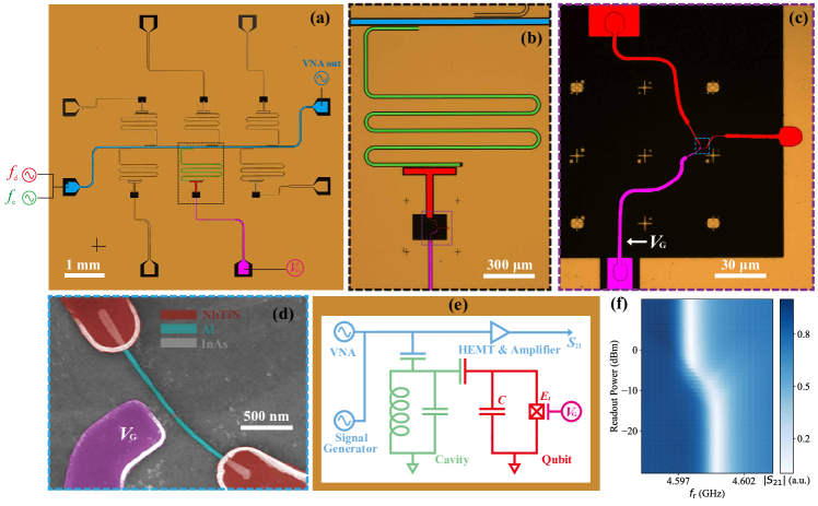
Qubit device and measurement circuit. Figure 1(a) shows the optical image (false colored) of the device chip. One gatemon qubit (device A, the dashed box) was measured with results shown in Figs. 2-4. The other five qubits on this chip were not working. We have characterized three working qubits, see the supplementary material (SM) for the other two. For the device fabrication, a 100-nm-thick NbTiN superconducting film (the orange region) was first sputtered onto a sapphire substrate. Reactive ion etching was then performed to etch away part of the film (the dark regions). This lithography step defines the co-planar wave-guide feed line (blue), the resonator/cavity (green) and the shunt capacitor of the gatemon (red). Figure 1(b) is a zoomed-in image of the qubit. The feed line capacitively couples to a cavity for the qubit readout. The cavity internal quality factor, , is 14000 and the bare resonance frequency is 4.6 GHz. The cavity further couples to the T-shape capacitor whose capacitance is estimated to be 100 fF. This capacitor connects to the InAs-Al nanowire Josephson junction (Figs. 1(c) and 1(d)) and together, they form the gatemon qubit. The large capacitance determines the charging energy to 190 MHz. The other side of the Josephson junction connects to the ground. A side gate (pink) tunes the junction transparency and therefore controls the Josephson energy, . The junction was defined by removing (etching) a small Al segment on the InAs wire (diameter 35 nm). Transports on these wires show a gate-tunable supercurrent () on the order of 100 nA [45]. The corresponding 50 GHz is much larger than . This ensures that the qubit can be operated in the transmon regime. For details of the device fabrication, circuit set-up and cavity calibration, see SM (the method session, Figs. S1 and S2).
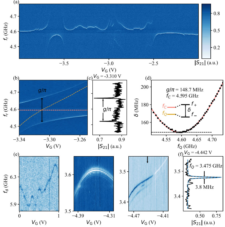
Figure 1(e) draws the equivalent circuit diagram. For the cavity and qubit readout, a microwave tone of frequency (near the cavity resonant frequency ) is applied to the feed line (see Fig. 1(a)). The transmission of this microwave tone, , is measured by a vector network analyzer (VNA). Figure 1(f) is such a “single-tone” measurement by sweeping and its power while monitoring the transmission amplitude . At high power, the qubit is “overwhelmed” and the dip in corresponds to the bare resonant frequency of the cavity [46]. At low power, the resonant frequency is qubit-state dependent due to the cavity-qubit dispersive interaction. The repulsion of the qubit and cavity causes the shift of the resonance frequency as shown in Fig. 1(f). To excite and control the qubit, a second microwave tone of frequency can be applied in the standard “two-tone” spectroscopy.
Vacuum Rabi splitting and qubit spectroscopy. In Fig. 2(a), we keep the readout power low and scan the gate voltage (). The resonant frequency of the cavity is gate tunable, indicating the presence of the gatemon. For better visibility, a signal background, contributed by standing waves in the circuit, was subtracted from (see Fig. S3 in SM for details). The jumps in the spectrum are due to charge instabilities in the InAs-Al devices which are also commonly observed in the transport characterizations. The qubit frequency () is given by the energy difference between the ground state and the first excited state, . tunes therefore controls . When is tuned close to the cavity frequency (), the strong qubit-cavity hybridization leads to the anti-crossings. This anti-crossing is observed in the single-tone spectrum shown in Fig. 2(a). See Fig. 2(b) for a fine scan (an enlargement) of an anti-crossing. Figure 2(c) is the line cut at = -3.310 V where the peak spacing is the smallest. In this strong coupling regime, the frequencies of the two peaks are . The peak spacing, , is a function of . The qubit frequency can be obtained by . Figure 2(d) plots the extracted and . The red line is the theory fit based on the formula above. We extract the qubit-cavity coupling strength 74 MHz.
Next we tune to bias away from and reach the dispersive regime. The large detuning, , could effectively suppress the energy relaxation due to the Purcell effect [47]. Figure 2(e) shows the two-tone spectroscopy, as a function of the qubit drive (the second tone) at three different ranges. The readout frequency (the first tone) was fixed near the cavity resonance (). When is scanned on resonance with , the qubit can be excited and the resonator frequency is shifted. A signal in the readout tone can be observed due to the cavity shift. The spectroscopy in Fig. 2(e) reveals the gate tunable nature of . The non-monotonic fluctuations are associated with the non-ballistic property of the InAs-Al junction, indicating the presence of disorder.
The multiple peaks in Fig. 2(e) are likely caused by the photon-number-dependent frequency shift of the qubit [48]. This is obvious when the cavity readout tone was continuously applied (instead of pulsed) on the feed line, see Fig. S4 in SM for detailed analysis. The extracted peak spacing (12 MHz) roughly matches our estimation of 10 MHz. Figure 2(f) shows a line cut of the qubit excitation peak from Fig. 2(e). From the Lorentzian fit we extract the full width at half maximum (FWHM 3.8 MHz). This width corresponds to a coherence time 0.26 s, consistent with the time-domain measurement in Figs. 3 and 4.
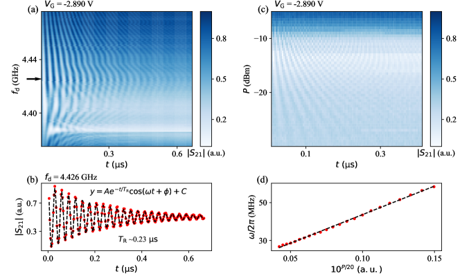
Rabi oscillations. We now manipulate the gatemon qubit in time domain. A qubit drive pulse () was first applied for a duration time of and then followed by a readout pulse of the cavity. Figure 3(a) shows the typical Rabi oscillations as a function of and . The Rabi oscillation frequency . The term, const., is proportional to the square of the driving amplitude. The oscillation pattern shows a Chevron feature. We note that the pattern gets disrupted near 4.40 GHz, probably due to the presence of another cavity on the chip whose resonant frequency is around 4.40 GHz. From Fig. 3(a), we can estimate the qubit frequency 4.426 GHz. Note that this is not in the dispersive regime yet since the detuning is not large enough. Figure 3(b) shows the line cut near . Fitting the decaying oscillation using an empirical formula (the dashed line), we extract the Rabi coherence time 0.23 s.
In Fig. 3(c), the qubit drive power is varied. Higher power drives the qubit faster, resulting in a shorter oscillation period. We extract the oscillation frequency (the inverse of the period) and plot it as a function of its driving amplitude (converted from the power) in Fig. 3(d). The dashed line is a linear fit, confirming its Rabi oscillation nature.
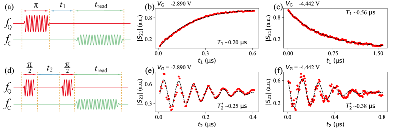
Gatemon quantum coherence. To extract the gatemon energy relaxation time , a pulse was first applied to excite the qubit to the state. The readout was performed after the waiting time (Fig. 4(a)). Figures 4(b) and 4(c) show the exponential fit at two different gate voltages. A relaxation time 0.56 s can be extracted. The dephasing time was determined by the Ramsey experiment: inserting a waiting time between two slightly detuned /2 pulses before the readout (Fig. 4(d)). Figures 4(e) and 4(f) show two Ramsey oscillations. can reach 0.38 s. The fitting assumes an exponential decaying envelope: [49]. Note that the gate voltage of Figs. 4(c) and 4(f) corresponds to the dispersive regime ( here is 3.446 GHz), therefore a longer coherence time is expected. As a comparison, the coherence times for Figs. 4(b) and 4(e) are shorter due to the Purcell effect. indicates that the coherence of our qubit is not entirely limited by energy relaxation. For the Rabi oscillations at = -4.442 V (same with Figs. 4(c) and 4(f)), see Fig. S5. In Fig. S6, we show the measurement of two more gatemon qubits.
In summary, we have studied the gatemon qubit based on a thin InAs-Al hybrid nanowire. The gatemon can reach strong coupling to a cavity. Coherent Rabi oscillations can be observed. The qubit relaxation time and dephasing time can reach 0.56 s and 0.38 s, respectively. Future work on these thin-wire-based gatemons could aim for possible Majorana signatures in a finite magnetic field.
Acknowledgment We thank Chunqing Deng and Luyan Sun for valuable discussions. We also thank the Teaching Center for Experimental Physics of Tsinghua University for using their equipment. This work is supported by Tsinghua University Initiative Scientific Research Program, Alibaba Innovative Research Program, National Natural Science Foundation of China (Grant Nos. 12204047, 92065106, 61974138). D.P. also acknowledges the support from Youth Innovation Promotion Association, Chinese Academy of Sciences (Nos. 2017156 and Y2021043). Raw data and processing codes within this paper are available at https://doi.org/10.5281/zenodo.7620737.
References
- Kitaev [2003] A. Kitaev, Fault-tolerant quantum computation by anyons, Annals of Physics 303, 2 (2003).
- Nayak et al. [2008] C. Nayak, S. H. Simon, A. Stern, M. Freedman, and S. Das Sarma, Non-abelian anyons and topological quantum computation, Rev. Mod. Phys. 80, 1083 (2008).
- Read and Green [2000] N. Read and D. Green, Paired states of fermions in two dimensions with breaking of parity and time-reversal symmetries and the fractional quantum hall effect, Phys. Rev. B 61, 10267 (2000).
- Kitaev [2001] A. Y. Kitaev, Unpaired majorana fermions in quantum wires, Physics-Uspekhi 44, 131 (2001).
- Lutchyn et al. [2010] R. M. Lutchyn, J. D. Sau, and S. Das Sarma, Majorana fermions and a topological phase transition in semiconductor-superconductor heterostructures, Phys. Rev. Lett. 105, 077001 (2010).
- Oreg et al. [2010] Y. Oreg, G. Refael, and F. von Oppen, Helical liquids and majorana bound states in quantum wires, Phys. Rev. Lett. 105, 177002 (2010).
- Mourik et al. [2012] V. Mourik et al., Signatures of majorana fermions in hybrid superconductor-semiconductor nanowire devices, Science 336, 1003 (2012).
- Deng et al. [2016] M. Deng et al., Majorana bound state in a coupled quantum-dot hybrid-nanowire system, Science 354, 1557 (2016).
- Gül et al. [2018] Ö. Gül et al., Ballistic majorana nanowire devices, Nature Nanotechnology 13, 192 (2018).
- Zhang et al. [2021] H. Zhang et al., Large zero-bias peaks in insb-al hybrid semiconductor-superconductor nanowire devices, arXiv: 2101.11456 (2021).
- Song et al. [2022] H. Song et al., Large zero bias peaks and dips in a four-terminal thin inas-al nanowire device, Phys. Rev. Research 4, 033235 (2022).
- Wang et al. [2022] Z. Wang et al., Plateau regions for zero-bias peaks within 5 of the quantized conductance value , Phys. Rev. Lett. 129, 167702 (2022).
- Prada et al. [2020] E. Prada et al., From andreev to majorana bound states in hybrid superconductor–semiconductor nanowires, Nature Reviews Physics 2, 575 (2020).
- Zhang et al. [2019] H. Zhang et al., Next steps of quantum transport in majorana nanowire devices, Nature Communications 10, 5128 (2019).
- Alicea et al. [2010] J. Alicea, Y. Oreg, G. Refael, F. Oppen, and M. Fisher, Non-abelian statistics and topological quantum information processing in 1d wire networks, Nature Physics 7 (2010).
- Hyart et al. [2013] T. Hyart, B. van Heck, I. C. Fulga, M. Burrello, A. R. Akhmerov, and C. W. J. Beenakker, Flux-controlled quantum computation with majorana fermions, Phys. Rev. B 88, 035121 (2013).
- Knapp et al. [2016] C. Knapp, M. Zaletel, D. E. Liu, M. Cheng, P. Bonderson, and C. Nayak, The nature and correction of diabatic errors in anyon braiding, Phys. Rev. X 6, 041003 (2016).
- Aasen et al. [2016] D. Aasen, M. Hell, R. V. Mishmash, A. Higginbotham, J. Danon, M. Leijnse, T. S. Jespersen, J. A. Folk, C. M. Marcus, K. Flensberg, and J. Alicea, Milestones toward majorana-based quantum computing, Phys. Rev. X 6, 031016 (2016).
- Plugge et al. [2017] S. Plugge, A. Rasmussen, R. Egger, and K. Flensberg, Majorana box qubits, New Journal of Physics 19, 012001 (2017).
- Vijay and Fu [2016] S. Vijay and L. Fu, Teleportation-based quantum information processing with majorana zero modes, Phys. Rev. B 94, 235446 (2016).
- Karzig et al. [2017] T. Karzig, C. Knapp, R. M. Lutchyn, P. Bonderson, M. B. Hastings, C. Nayak, J. Alicea, K. Flensberg, S. Plugge, Y. Oreg, C. M. Marcus, and M. H. Freedman, Scalable designs for quasiparticle-poisoning-protected topological quantum computation with majorana zero modes, Phys. Rev. B 95, 235305 (2017).
- Koch et al. [2007] J. Koch, T. M. Yu, J. Gambetta, A. A. Houck, D. I. Schuster, J. Majer, A. Blais, M. H. Devoret, S. M. Girvin, and R. J. Schoelkopf, Charge-insensitive qubit design derived from the cooper pair box, Phys. Rev. A 76, 042319 (2007).
- Houck et al. [2007] A. Houck, D. Schuster, J. Gambetta, J. Schreier, B. Johnson, J. Chow, L. Frunzio, J. Majer, M. Devoret, S. Girvin, and R. Schoelkopf, Generating single microwave photons in a circuit, Nature 449, 328 (2007).
- Ginossar and Grosfeld [2014] E. Ginossar and E. Grosfeld, Microwave transitions as a signature of coherent parity mixing effects in the majorana-transmon qubit, Nature communications 5, 4772 (2014).
- Yavilberg et al. [2015] K. Yavilberg, E. Ginossar, and E. Grosfeld, Fermion parity measurement and control in majorana circuit quantum electrodynamics, Phys. Rev. B 92, 075143 (2015).
- Li et al. [2018] T. Li, W. A. Coish, M. Hell, K. Flensberg, and M. Leijnse, Four-majorana qubit with charge readout: Dynamics and decoherence, Phys. Rev. B 98, 205403 (2018).
- Ávila et al. [2020] J. Ávila, E. Prada, P. San-Jose, and R. Aguado, Majorana oscillations and parity crossings in semiconductor nanowire-based transmon qubits, Phys. Rev. Research 2, 033493 (2020).
- Chirolli et al. [2022] L. Chirolli, N. Y. Yao, and J. E. Moore, Swap gate between a majorana qubit and a parity-protected superconducting qubit, Phys. Rev. Lett. 129, 177701 (2022).
- Larsen et al. [2015] T. W. Larsen, K. D. Petersson, F. Kuemmeth, T. S. Jespersen, P. Krogstrup, J. Nygård, and C. M. Marcus, Semiconductor-nanowire-based superconducting qubit, Phys. Rev. Lett. 115, 127001 (2015).
- de Lange et al. [2015] G. de Lange, B. van Heck, A. Bruno, D. J. van Woerkom, A. Geresdi, S. R. Plissard, E. P. A. M. Bakkers, A. R. Akhmerov, and L. DiCarlo, Realization of microwave quantum circuits using hybrid superconducting-semiconducting nanowire josephson elements, Phys. Rev. Lett. 115, 127002 (2015).
- Casparis et al. [2016] L. Casparis, T. W. Larsen, M. S. Olsen, F. Kuemmeth, P. Krogstrup, J. Nygård, K. D. Petersson, and C. M. Marcus, Gatemon benchmarking and two-qubit operations, Phys. Rev. Lett. 116, 150505 (2016).
- Luthi et al. [2018] F. Luthi, T. Stavenga, O. W. Enzing, A. Bruno, C. Dickel, N. K. Langford, M. A. Rol, T. S. Jespersen, J. Nygård, P. Krogstrup, and L. DiCarlo, Evolution of nanowire transmon qubits and their coherence in a magnetic field, Phys. Rev. Lett. 120, 100502 (2018).
- Kringhøj et al. [2020] A. Kringhøj, B. van Heck, T. W. Larsen, O. Erlandsson, D. Sabonis, P. Krogstrup, L. Casparis, K. D. Petersson, and C. M. Marcus, Suppressed charge dispersion via resonant tunneling in a single-channel transmon, Phys. Rev. Lett. 124, 246803 (2020).
- Bargerbos et al. [2020] A. Bargerbos, W. Uilhoorn, C.-K. Yang, P. Krogstrup, L. P. Kouwenhoven, G. de Lange, B. van Heck, and A. Kou, Observation of vanishing charge dispersion of a nearly open superconducting island, Phys. Rev. Lett. 124, 246802 (2020).
- Larsen et al. [2020] T. W. Larsen, M. E. Gershenson, L. Casparis, A. Kringhøj, N. J. Pearson, R. P. G. McNeil, F. Kuemmeth, P. Krogstrup, K. D. Petersson, and C. M. Marcus, Parity-protected superconductor-semiconductor qubit, Phys. Rev. Lett. 125, 056801 (2020).
- Sabonis et al. [2020] D. Sabonis, O. Erlandsson, A. Kringhøj, B. van Heck, T. W. Larsen, I. Petkovic, P. Krogstrup, K. D. Petersson, and C. M. Marcus, Destructive little-parks effect in a full-shell nanowire-based transmon, Phys. Rev. Lett. 125, 156804 (2020).
- Bargerbos et al. [2022] A. Bargerbos et al., Singlet-doublet transitions of a quantum dot josephson junction detected in a transmon circuit, PRX Quantum 3, 030311 (2022).
- Caroff et al. [2009] P. Caroff, K. A. Dick, J. Johansson, M. E. Messing, K. Deppert, and L. Samuelson, Controlled polytypic and twin-plane superlattices in iii-v nanowires, Nature nanotechnology 4, 50 (2009).
- Shtrikman et al. [2009] H. Shtrikman, R. Popovitz-Biro, A. Kretinin, L. Houben, M. Heiblum, M. Bukała, M. Galicka, R. Buczko, and P. Kacman, Method for suppression of stacking faults in wurtzite iii- v nanowires, Nano letters 9, 1506 (2009).
- Pan et al. [2014] D. Pan et al., Controlled synthesis of phase-pure inas nanowires on si (111) by diminishing the diameter to 10 nm, Nano letters 14, 1214 (2014).
- Pientka et al. [2012] F. Pientka, G. Kells, A. Romito, P. W. Brouwer, and F. Von Oppen, Enhanced zero-bias majorana peak in the differential tunneling conductance of disordered multisubband quantum-wire/superconductor junctions, Physical review letters 109, 227006 (2012).
- Rainis et al. [2013] D. Rainis, L. Trifunovic, J. Klinovaja, and D. Loss, Towards a realistic transport modeling in a superconducting nanowire with majorana fermions, Physical Review B 87, 024515 (2013).
- Pan and Das Sarma [2020] H. Pan and S. Das Sarma, Physical mechanisms for zero-bias conductance peaks in majorana nanowires, Phys. Rev. Research 2, 013377 (2020).
- Pan et al. [2022] D. Pan et al., In situ epitaxy of pure phase ultra-thin inas-al nanowires for quantum devices, Chinese Physics Letters 39, 058101 (2022).
- Wang et al. [2023] Z. Wang et al., Supercurrent in a quasi-ballistic thin inas-al hybrid nanowire device, to be appeared (2023).
- Reed et al. [2010] M. D. Reed, L. DiCarlo, B. R. Johnson, L. Sun, D. I. Schuster, L. Frunzio, and R. J. Schoelkopf, High-fidelity readout in circuit quantum electrodynamics using the jaynes-cummings nonlinearity, Phys. Rev. Lett. 105, 173601 (2010).
- Purcell et al. [1946] E. M. Purcell, H. C. Torrey, and R. V. Pound, Resonance absorption by nuclear magnetic moments in a solid, Phys. Rev. 69, 37 (1946).
- Schuster et al. [2007] D. Schuster, A. Houck, J. Schreier, A. Wallraff, J. Gambetta, A. Blais, L. Frunzio, J. Majer, B. Johnson, M. Devoret, S. Girvin, and R. Schoelkopf, Resolving photon number states in a superconducting circuit, Nature 445, 515 (2007).
- Krantz et al. [2019] P. Krantz, M. Kjaergaard, F. Yan, T. P. Orlando, S. Gustavsson, and W. D. Oliver, A quantum engineer’s guide to superconducting qubits, Applied Physics Reviews 6, 021318 (2019).
See pages 1 of SM_gatemon.pdf See pages 2 of SM_gatemon.pdf See pages 3 of SM_gatemon.pdf See pages 4 of SM_gatemon.pdf See pages 5 of SM_gatemon.pdf