Observation of a Pinched-Loop in a Current-Excited Inductive Circuit
Abstract
In this work, we show that a pinched-loop can be observed in the voltage-current plane when a series R-L circuit is current excited. Specifically, the resistance (R) in this circuit is variable and is voltage-controlled by the voltage developed across the inductor due to the exciting current. In this context, we confirm our previous results that the pinched-loop is not a characteristic of memrsitors or memrsitive systems and that it can be observed in many other nonlinear systems. Numerical simulations, circuit simulations and experimental results validate the theory.
I Introduction
Memristors have been studied as new electronic devices with promising analog/digital and neuromorphic applications [1, 2, 3]. Their characteristic behavior is a pinched-loop in the current-voltage plane [4]. This behavior however has been shown to exist in other nonlinear devices such as a non-linear inductor or a non-linear capacitor [5], and that its appearance is linked to satisfying the necessary conditions of the theory of Lissajous figures [6]. The pinched-loop is a Lissajous figure of order two; i.e. with one point of intersection (also known as the pinch point). To generate such a figure from two signals, one of them must contain a harmonic component with twice the frequency of the other signal. In addition, the phase shift between this harmonic and the fundamental frequency component must not exceed [6]. Without using a nonlinear device, the frequency-doubling mechanism mandated by the theory of Lissajous figures, cannot be generated from an applied input signal (voltage or current) with a fixed frequency. We have recently verified this fact using commercially available memristor devices in [7] where we have shown that the measured memristor current signal does indeed contain a strong harmonic component at twice the frequency of the applied voltage signal. This harmonic is the only one needed to generate the pinched-loop and therefore all other higher-order harmonics can be filtered out from the current signal [7].
In this work, we show that a current excited series R-L network can also generate a pinched-loop if the resistor is nonlinear and voltage-controlled by the voltage developed across the inductor resulting from the current excitation. This forms a kind of self-feedback state-control which in-directly implements a multiplication operation. This multiplication operation generates a harmonic component (in the voltage developed across the R-L circuit) with twice the frequency of the applied input current signal. The proposed concept is validated using a simple circuit implementation that relies on a junction field effect transistor (JFET) operating as a voltage-controlled resistor. When compared to other similar concepts in the literature [8], the robustness and simplicity of this work become apparent. An experimental verification using a Field Programmable Analog Array (FPAA) of the proposed concept is also provided.
II Theory
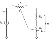
Consider the circuit shown in Fig. 1 composed of an inductor in series with a resistor which has a fixed part () and a variable part (). The network is excited by a current source () and the developed voltage on the network () is measured. The variable resistance is voltage-controlled by the inverted voltage developed on the inductor; i.e. or a scaled (by factor ) version of this voltage. Therefore, the total resistance of the network is given by
| (1) |
where is an arbitrary reference voltage to ensure proper dimensions. The input voltage measured across the network is therefore given by
| (2) |
The above equation can be transformed into dimensionless form after defining , , , and using the normalized time . We thus obtain the following equation
| (3) |
The second term in the above equation represents a clear multiplication operation without need for a physical multiplier. This operation is the key behind the frequency-doubling mechanism and hence generating the pinched-loop as demonstrated below.
(a)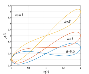
(b)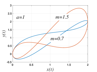
(c) 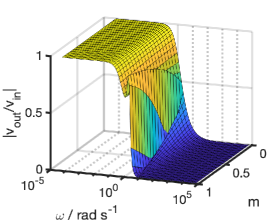
Numerical simulation results of equation (3) are shown in Fig. 2(a) for and three different values of . Here, with for simplicity. The pinched-loop behavior can clearly be obtained from equation (3) and the pinch point is located at . The loop is always symmetrical in this case whereas in Fig. 2(b), non-symmetrical loops are observed for and . Specifically, two results are shown for and . The generation of the pinched-loop in (3) can be attributed to the frequency doubling mechanism resulting from the term. For , the system is described by the two parametric equations
| (4) |
and at the pinch-point , the phase shift between the two signals is satisfying the Lissajous condition for creating a pinched-loop. It can also be shown in this case that
| (5) |
and hence
| (6) |
Therefore, the infliction point at is located at with the corresponding value of , as expected. Note however that the second term in (5) cancels out at and at . Therefore, there are two more points at which which are and . These two points are clearly visible in Fig. 2(a) for . In fact, for any value of and , the pinched loop always passes through the two points and as clear from Fig. 2(a,b).
It is worth mentioning that taking the voltage across the resistor in Fig. 1 as an output ( and considering the magnitude response of ; where shows a classical low-pass filter response with a cutoff frequency when . Now with , it is seen that the normalized output voltage is equal to . Therefore assuming that , it can be shown that
| (7) |
since and time is normalized with respect to , it can be seen that the low-pass filter transfer function at is as expected. Figure 2(c) shows the magnitude response of (7) for different values of and for .
III Circuit Verification
III-A with discrete components
It is possible to realize the circuit in Fig. 1 using a JFET as a voltage-controlled resistor as shown in Fig. 3. Here, a fixed resistor is used as whereas the current feedback op amp (CFOA) is used as a differential amplifier to obtain the voltage developed across the inductor and re-inject it to the gate terminal of the JFET device. The control voltage for the JFET resistance is thus equal to . Meanwhile, op amp is another CFOA used as a voltage-to-current converter in order to obtain the excitation current through its high impedance current output terminal.
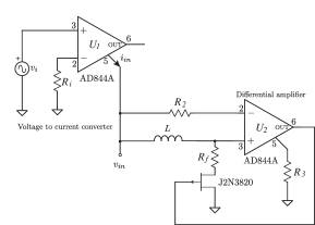
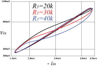
Using an AD844 CFOA device and a J2N3820 JFET device, the Spice simulated response of the circuit is plotted in Fig. 4 depicting versus for three different ratios of namely and . The inductor was chosen as and had an amplitude of with a DC offset voltage of and a frequency of . The nominal resistance of the JFET was measured as and therefore the circuit simulations correspond to in the numerical simulations. We noted that at , a symmetrical loop is observed (see red loop in Fig. 4) whereas for a lower and a higher value, the loop is not symmetrical. Therefore, plays the role of and controls the loop symmetry when .
III-B with a Field Programmable Analog Array
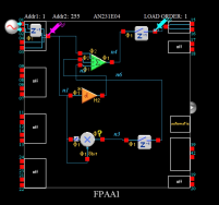
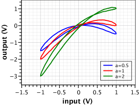
For experimental verification, the AN231E04 FPAA from Anadigm was employed to validate the concept described by (3). The board is programmed through the AnadigmDesigner®2 EDA software, and the tested configuration is depicted in Fig. 5, where the Hold, SumDiff (summation stage), Differentiator and Multiplier CAMs are utilized. The clock frequency was set to 100kHz, while the system is stimulated by a 1KHz, 1V input signal. Considering that and the results of the synthesis of the input and output waveforms are demonstrated in Fig. (6a), while the corresponding results for and are provided in Fig. (6b). The skewness in the pinched-loops is attributed to the limited dynamic range of the FPAA.

IV Discussion
We stress that pinched-loop behavior can only exist in nonlinear circuits and systems meaning that any fabricated solid-state device that shows a pinched-loop must have an embedded form of state-controlled nonlinearity; most likely a voltage- or current-controlled resistor or transconductor. In this regards, it is important to recall that an inductor may exist in the form of a parasitic element not intentionally inserted in series with a voltage-controlled resistor. If the voltage developed across this inductor leaks to the resistor (e.g. through magnetic coupling), it may then cause the appearance of the pinched-loop behavior. Interestingly, in the very recent work of [9], the author show that “the halide perovskite memristor response contains the composition of two inductive processes”. Therefore, the existence of inductive behavior in nano-materials is not unusual.
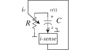
Furthermore, applying the duality principle to the circuit in Fig. 1, it can be established that a voltage-excited parallel R-C circuit where the resistor is controlled by the current developed inside the capacitor as a result of the applied voltage excitation will lead to similar results; i.e. observation of pinched-loops. This dual circuit is depicted in Fig. 7 where a current sensing mechanism can be used to sense the current in the capacitor and re-use it to control the parallel resistor. In solid-state devices, this may naturally occur through leakage. In fact, the work of [10] has already shown that in a memristor device, there must exist two capacitors ( and ) parallel to the switch on and switch off resistances ( and ) (see Fig. 5 of [10]) leading to the conclusion of that work that “memory resistance and memory capacitance” must co-exist. From a circuit theoretical point of view, it is known that in order to measure a voltage it must be held on a capacitor for the duration of the measurement. If this voltage is across a resistor, then there must exist a physical or a parasitic capacitor to hold this voltage. Therefore, it is literally impossible to ignore the capacitive effect particularly in nano-scale devices [11]. In fact, we beg to argue that the pinched-loop observed in nano-devices is either via an inductive effect (following for example the topology of Fig. 1 above [9]) or via a capacitive effect (following the topology of the dual circuit in Fig. 7, for example [10]). The talk about a capacitance-free and/or inductance-free mem(resistor) is fundamentally in-correct and obstructs the understanding of the true mechanisms by which a pinched-loop can be created [6] [12].
V Conclusion
We investigated a new concept for generating pinched loops using the current excitation of an inductive circuit. This work is a further contribution to the body of research that confirms that pinched hysteresis loops are not unique to memristors [13] and are not finger-prints of these devices as unfortunately widely advocated. In addition, the question of whether the memristor is or is not a fundamental element has been addressed by several authors (see for example [14, 15]). In practice, the link between magnetic flux and electric charge implies that one of them is the cause and the other is the measurable effect. If the electric charge (magnetic flux) is the cause, then there must exist a capacitive (inductive) effect by which this charge (flux) is transported. Whether a pinched-loop is observed or not is absolutely governed by satisfying the theory of Lissajous figures [16, 17] between the current and voltage signals.
References
- [1] B. Chen, H. Yang, F. Zhuge, Y. Li, T. Chang, Y. He, W. Yang, N. Xu, and X. Miao, “Optimal tuning of memristor conductance variation in spiking neural networks for online unsupervised learning,” IEEE Trans. Electron Devices, vol. 66, pp. 2844–2849, June 2019.
- [2] Y. Zhao, C. Fang, X. Zhang, X. Xu, T. Gong, Q. Luo, C. Chen, Q. Liu, H. Lv, Q. Li, F. Zhang, L. Li, and M. Liu, “A compact model for drift and diffusion memristor applied in neuron circuits design,” IEEE Trans. Electron Devices, vol. 65, pp. 4290–4296, Oct 2018.
- [3] L. Ge, W. Xuan, S. Liu, S. Huang, X. Wang, S. Dong, H. Jin, and J. Luo, “Biomaterial Gelatin film based crossbar structure resistive switching devices,” IEEE Transactions on Nanotechnology, vol. 17, pp. 78–83, Jan 2018.
- [4] A. Elwakil, M. Fouda, and A. Radwan, “A simple model of double-loop hysteresis behavior in memristive elements,” IEEE Trans. Circuits and Systems II: Express Briefs, vol. 60, no. 8, pp. 487–491, 2013.
- [5] M. E. Fouda, A. S. Elwakil, and A. G. Radwan, “Pinched hysteresis with inverse-memristor frequency characteristics in some nonlinear circuit elements,” Microelectronics Journal, vol. 46, no. 9, pp. 834–838, 2015.
- [6] B. Maundy, A. S. Elwakil, and C. Psychalinos, “Correlation between the theory of lissajous figures and the generation of pinched hysteresis loops in nonlinear circuits,” IEEE Trans. Circuits and Systems I: Regular Papers, vol. 66, no. 7, pp. 2606–2614, 2019.
- [7] S. Majzoub, A. Elwakil, C. Psychalinos, and B. Maundy, “On the mechanism of creating pinched hysteresis loops using a commercial memristor device,” AEU - Int. J. Electronics and Communications, vol. 111, p. 152923, 2019.
- [8] A. G. Alharbi, M. E. Fouda, Z. J. Khalifa, and M. H. Chowdhury, “Electrical nonlinearity emulation technique for current-controlled memristive devices,” IEEE Access, vol. 5, pp. 5399–5409, 2017.
- [9] M. Berruet, J. C. Pérez-Martínez, B. Romero, C. Gonzales, A. M. Al-Mayouf, A. Guerrero, and J. Bisquert, “Physical model for the current–voltage hysteresis and impedance of halide perovskite memristors,” ACS Energy Letters, vol. 7, no. 3, pp. 1214–1222, 2022.
- [10] I. Salaoru, Q. Li, A. Khiat, and T. Prodromakis, “Coexistence of memory resistance and memory capacitance in tio2 solid-state devices,” Nanoscale Research Letters, vol. 9, no. 1, p. 552, 2014.
- [11] S. Zhu, B. Sun, S. Ranjan, X. Zhu, G. Zhou, H. Zhao, S. Mao, H. Wang, Y. Zhao, and G. Fu, “Mechanism analysis of a flexible organic memristive memory with capacitance effect and negative differential resistance state,” APL Materials, vol. 7, no. 8, p. 081117, 2019.
- [12] B. Xu, C. Paillard, B. Dkhil, and L. Bellaiche, “Pinched hysteresis loop in defect-free ferroelectric materials,” Phys. Rev. B, vol. 94, p. 140101, Oct 2016.
- [13] L. Chua, “If it is pinched it is a memristor,” Semiconductor Science and Technology, vol. 29, no. 10, p. 104001, 2014.
- [14] I. Abraham, “The case for rejecting the memristor as a fundamental circuit element,” Scientific reports, vol. 8, no. 1, p. 10972, 2018.
- [15] B. Tellini, M. Bologna, K. J. Chandía, and M. Macucci, “Revisiting the memristor concept within basic circuit theory,” International Journal of Circuit Theory and Applications, vol. 49, no. 11, pp. 3488–3506, 2021.
- [16] J. Wang, G. Zhang, and Z. You, “Design rules for dense and rapid lissajous scanning,” Microsystems & Nanoengineering, vol. 6, no. 1, p. 101, 2020.
- [17] A. Figueroa, S. Cuevas, and E. Ramos, “Lissajous trajectories in electromagnetically driven vortices,” Journal of Fluid Mechanics, vol. 815, pp. 415–434, 2017.