Scientific CMOS sensors in Astronomy: IMX455 and IMX411
Abstract
Scientific complementary metal-oxide-semiconductor (CMOS) detectors have developed quickly in recent years thanks to their low cost and high availability. They also have some advantages over charge-coupled devices (CCDs), such as high frame rate or typically lower readout noise. These sensors started to be used in astronomy following the development of the first back-illuminated models. Therefore, it is worth studying their characteristics, advantages, and weaknesses. One of the most widespread CMOS sensors are those from the Sony IMX series, which are included in large astronomical survey projects based on small and fast telescopes because of their low cost, and capability for wide-field and high-cadence surveys. In this paper, we aim to characterize the IMX455M and IMX411M sensors, which are integrated into the QHY600 and QHY411 cameras, respectively, for use in astronomical observations. These are large (36 24 and 54 40 mm) native 16 bit sensors with 3.76 m pixels and are sensitive in the optical range. We present the results of the laboratory characterization of both cameras. They showed a very low dark current of 0.011 and 0.007 e- px-1 s-1 @–10°C for the QHY600 and QHY411 cameras, respectively. They also show the presence of warm pixels, 0.024% in the QHY600 and 0.005% in the QHY411. Warm pixels proved to be stable and linear with exposure time, and are therefore easily corrected using dark frames. Pixels affected by the Salt & Pepper noise are 2% of the total and a method to correct for this effect is presented. Both cameras were attached to night telescopes and several on-sky tests were performed to prove their capabilities. On-sky tests demonstrate that these CMOS behave as well as CCDs of similar characteristics and (for example) they can attain photometric accuracies of a few milli-magnitudes.
PASP
1 Introduction
Historically, observational astronomy has been determined by the development of imaging technology. In the early twentieth century, the introduction of the photographic plate marked an unprecedented revolution, but their very limited quantum efficiency (QE) of 0.1% made it imperative to develop more effective alternatives. The turning point came in 1969 with the appearance of charge-coupled devices (CCDs, Boyle & Smith (1970)), which are silicon-based sensors with two-dimensional arrays of photosensitive units (pixels). These devices produced improved linearity and quantum efficiency over photographic plates and simplified data analysis thanks to their analog-to-digital conversion (ADC). The first astronomical image that was taken with a CCD appeared in 1975 when scientists from NASA’s Jet Propulsion Laboratory obtained an image of the planet Uranus at a wavelength of 8900 Å (Janesick et al., 1987). The development and refinement of CCDs have increasingly made these sensors the most widely used option for the manufacture of astronomical instruments.
Over the last two decades, the rise of alternative technologies has undermined the prevalence of CCD sensors. Complementary metal-oxide-semiconductor (CMOS) image sensors started to be developed in the 1990s (Fossum, 1997). However, they still had a number of disadvantages when compared with CCDs, such as lower dynamic range (DR), and poorer linearity and sensitivity (Bigas et al., 2006). Although CMOS sensors soon established themselves in the consumer market, their inherent constraints restricted their application in certain fields, especially those related to science. To overcome the typical limitations of CMOS, the so-called scientific CMOS (sCMOS) were introduced in 2009 as a result of a collaboration between Andor Technology, Fairchild Imaging (BAE Systems) and PCO Imaging (Coates et al., 2009). This new generation of sensors combined high frame rates, reasonable pixel and sensor sizes, and quantum efficiencies comparable to CCDs—especially back-illuminated (BI) sCMOS (Princeton Instruments, 2016)—and a considerable reduction in the noise levels that are traditionally associated with CMOS.
Scientific CMOS are beginning to be accepted in astronomy. The first analyses in this respect mainly involve two sensors: CIS2051 (later rebranded as CIS2521), which was developed by Andor Technology and integrated into the Neo series detectors; and GSENSE, which was developed by Gpixel and integrated by several companies, e.g., Finger Lakes Instrumentation, QHYCCD, and Andor Technology. Experiments performed with Andor Neo showed low readout noise (1 e-) and linearity deviations up to the saturation point within the expected range of 1%. However, two features were noticed: the transfer curve was observed to bend, even at low signal levels, which was possibly caused by the non-linearity of an amplifier stage; and the signal shows certain irregularities with high variance in the transition region between high and low gain modes (Schildknecht et al., 2013). This, along with a limited QE due to being front-illuminated and a lower fill factor (Qiu et al., 2013), means that this sensor is not the most suitable for regular observations, and its usefulness is mostly constrained to bright objects and high frame rates. The back-illuminated GSENSE2020 sensor, integrated in the Andor Marana, was recently tested for its application in astronomy by Qiu et al. (2021) and Karpov et al. (2021). This sensor showed a low readout noise (1.6 e-), good linearity (), and a stable bias. This sensor family has a dual-amplifier structure in which two 12 bit images are taken simultaneously and are then merged into a single 16 bit high dynamic range image. However, this mechanism is susceptible to jumps and instabilities around the transition region between high and low gain. In addition, edge glowing and charge persistence over long periods of time is also present. The capabilities of these sensors decrease considerably with exposure times longer than several seconds, which is a consequence of these effects and the increase of dark current; however, they are still suitable instruments for high frame rate observations.
Many leading manufacturers are now developing instrumentation based on next-generation sCMOS sensors, but their suitability for general use in astronomy is still largely unexplored. One of the most widespread sensors are those from the Sony IMX series, which are being included in large projects such as the Argus Optical Array (Law et al., 2022), Large Array Survey Telescope (Ofek et al., 2023) or the next generation of telescopes for the ATLAS project (Tonry et al., 2018) , such as the one that will be installed at Teide Observatory, ATLAS-Teide (Licandro et al., 2023a), because of their low cost and capability for wide-field and high-cadence surveys.
In this paper, we present the results of the laboratory characterization of the sCMOS BI Sony IMX455M and IMX411M sensors when integrated into the QHY600M and QHY411M cameras. In Section 2, the two devices are tested, and the laboratory set-up and the telescopes that we used are presented. Sections 3.1 and 3.2 describe the tests performed under dark conditions: spatio-temporal variation of bias and dark and contaminating effects, such as random telegraph noise and the presence of warm pixels. In Section 3.3, the main operating features such as the gain fix pattern noise and linearity are verified using the photon transfer curve. The quantum efficiency measures are shown in Section 3.4 and the charge persistence effect reported in other sCMOS sensors is reviewed in Section 3.5. Finally, several approaches to processing telescope data and on-sky results based on this analysis are discussed in Section 5.
| Feature | QHY600M Pro | QHY411M |
|---|---|---|
| Sensor | Sony BI IMX455M | Sony BI IMX411M |
| Sensor size (diagonal) | 43.3 mm | 66.7 mm |
| Pixel size | 3.76 3.76 m | |
| Pixel area | 9600 6422 | 14304 10748 |
| Effective pixels | 61.17 Mpx | 151 Mpx |
| Max full frame rate | ||
| (USB 3.0 port, full frame | ||
| and 16-bit output) | 2.5 fps | 1 fps |
| A/D sample depth | ||
| (11 binning) | 16–bit | |
| Shutter type | Rolling shutter | |
| Cooling system | ||
| (temperatures below ambient) | Air cooling (-30C) | Air cooling (-35C) |
| Water cooling (-45C) | ||
2 Methods
2.1 Instruments
The QHY600M111https://www.qhyccd.com/scientific-camera-qhy600pro-imx455/ camera is based on the back-illuminated IMX455 monochrome sensor that is manufactured by SONY, which is a full-frame (35 mm format) sensor with , 3.76 m square pixels. The QHY411M222https://www.qhyccd.com/scientific-camera-qhy411-qhy461/ camera is based on SONY’s IMX411 monochrome sensor, which is also backilluminated but with a larger sensor size, (equivalent to medium-format cameras, mm). Both of these sensors include an overscan region of 33 and 91 rows, respectively, and they are native ADC sampled at 16 bit, which is a significant change from previous generations of sCMOS sensors that were based on 12 bit image merging (see Karpov et al. (2021)). The main features of the cameras are listed in Table 1. We used the QHY600M Pro version, which allows a faster Gbps fiber connection to a frame grabber with an additional 4 GB of DDR3 memory—although in this paper all tests were done via USB 3.0 connection—and triggering the rolling shutter via an external GPS with an accuracy of more than a microsecond. It is worth mentioning that both sensors, especially the IMX455, are used in cameras from other manufactures, e.g., Atik Apx60, ZWO ASI6200MM Pro.
These cameras can operate in several modes and gain settings, which essentially change their gain, readout noise (RON), and full-well capacity (FWC). In this paper, we have focused on those that are considered most appropriate for use in astronomy because they maintain a good balance between these characteristics, which are Mode#1 (High Gain Mode) and gain setting 0 (hereafter, #1@0) on the QHY600M Pro and Mode #4, and gain setting 0 (hereafter, #4@0) on the QHY411M, although some results for other modes are also shown.
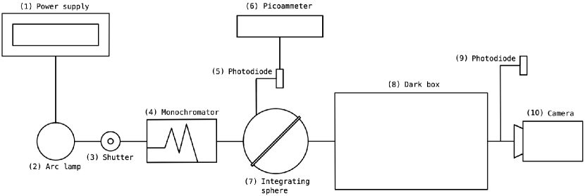
2.2 Optical test bench
The evaluation of the sensors was performed using existing experimental equipment, which are available at the Laboratory of Imaging and Sensors for Astronomy (LISA), at the Instituto de Astrofísica de Canarias (Tenerife, Spain). The set-up is schematically shown in Figure 1. A Newport M-66881 QTH lamp was connected to A Newport 68945 digital power supply, with intensity stabilization. In the Newport Oriel Cornerstone monochromator, the option to apply an order sorting filter was selected. This filter blocked higher diffraction orders from interfering with the selected wavelengths. A Newport 76994 shutter was placed between the lamp and the monochromator to control the light beam before taking each dark frame. A Labsphere US-080-SF/SL integrating sphere, placed next to the monochromator, had incorporated a Hamamatsu S1336-5B1 photodiode, which was in turn connected to a Keysight B2980A picoammeter. Next, a dark box was located, followed by the test of the camera. A second photodiode (Hamamatsu S2281) was connected to the exit port of the dark box. The conversion factors between the intensity measured by the picoammeter on the first photodiode and the radiant power received on the second photodiode at the exit of the dark box were characterized, in addition to the correction to the distance between the photodiode and the sensor back focus. During the tests, the laboratory temperature was about C and the humidity was 40–50%. Both cameras were air-cooled, with operating temperatures of C for the QHY600M Pro and C for the QHY411M.
2.3 Telescopes
The sky tests were performed with two of the robotic telescopes (Telescopios Abiertos Robticos, TAR) of Teide Observatory (Tenerife, Canary Islands, Spain). The QHY600M Pro was installed on the prime focus of TAR03, 0.46-m /2.8 C18 reflector telescope on a Planewave L500 altaz mount. An ROI of was used, giving a FOV of with px-1. The QHY411M was mounted on a Meade LX200-ACF 16′′ 0.406-m /10, on an APM GE-300 Direct Drive equatorial mount, with UV/IR-Cut/L, SDSS g′, r′ and i′ 50 mm filterswhich were manufactured by Baader Planetarium GmbH. The sensor was trimmed to mm, giving a FOV of arcmin with 0.40′′ px-1. Both cameras were connected via USB 3.0 and operated with air cooling at C. After the first tests, the QHY411M was installed in one of the 80 cm telescopes of the Two-meter Twin Telescope (TTT) project, which is a 0.80-m /6.85 Ritchey–Chrétien altaz telescope that was manufactured by ASA Astrosysteme GmbH, with a total FOV of and a plate scale of px-1.
3 Results
3.1 Bias stability and ”Salt & Pepper” effect
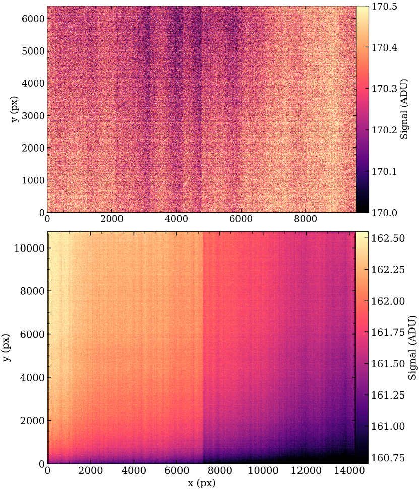
The bias frame stability in both cameras was tested in the laboratory under conditions of complete darkness. In all of the tests that are presented here, including the telescope runs, the offset setting was fixed at 10. First, 21 continuous unbinned full frames bias were obtained and stacked with a 3-clipping median to obtain the master bias. The result is shown in Figure 2. Both cameras show dark signal non-uniformity (DSNU), with a notable column-to-column pattern and pixel-to-pixel variations. Gradients can be observed in the QHY600M Pro toward the upper region, with variations of less than 1 ADU, especially in the QHY411M, with more than 2 ADU of difference between the upper left-hand and the lower right-hand corner.
In the readout process of typical CCDs, the charge is transferred to one—or several in the case of large sensors—output channels, each with a high-quality amplifier and an analog-to-digital converter (ADC). In contrast, in CMOS, each pixel has its own built-in electronics, which contain an amplifier and ADC. This allows a very high frame rate by parallelizing the readout process but exposes the sensor to these kinds of pixel-to-pixel variations, both in darkness (with different readout or thermal noises) and illuminated (with variations in gain or quantum efficiency). In sCMOS, each pixel must be understood as an independent sensor, so all corrections over them, such as subtraction of the bias level, must be done while bearing in mind that there is no single value that characterizes all of the pixels simultaneously. For this reason, although the QHY600M Pro and QHY411M have an overscan region, it is more accurate to use a full frame master bias or dark that takes into consideration these non-uniformities between pixels.
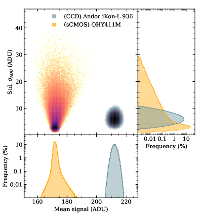
Once the spatial behavior of each pixel in darkness has been revised, the same 21 bias frames of the QHY411M are used to see its temporal performance in detail. Now, instead of taking the three-clipped median, the unclipped standard deviation and mean signal are plotted against each other, for every single pixel, in the left-hand plot of Figure 3. This shows that most of the pixels are found in a circular zone with a well-determined average signal between 170 and 175 ADU, corresponding to the median bias value, and with a standard deviation below 4 ADU. However, about 11% of the pixels show a temporal standard deviation that is higher than this value and also present deviations in the mean signal, with a kite-shaped dispersion. If this scatter were caused by pixels exhibiting higher values of read noise only, then the points would be distributed vertically, like a gradated column. If, however, the pixels had a different threshold voltage, i.e., bias level, but maintained the RON, then the points would be distributed horizontally. Instead, the kite-shape indicates that either both occur at the same time for these pixels or that there is an additional anomalous behavior at play.
For comparison, the same number of frames was taken with a CCD, the ANDOR iKon-L 936 BEX2-DD333https://andor.oxinst.com/assets/uploads/ products/andor/documents/andor-ikon-l-936-specifications.pdf, and the standard deviation and temporal average of each pixel was also obtained. The kite-shaped dispersion is not visible in this case. Furthermore, the histograms along both axes show the expected Gaussian shape: on the standard axis, a peak centered on the RON value; and on the mean signal axis, a peak centered on the average bias level and a width equal to the RON/. In the case of the QHY411M—the same behavior is observed in the QHY600M Pro—the histograms show a narrow peak and tails toward high standard deviation. This implies that most of the pixels show a low RON, but some others have a skewed signal on both sides of the average bias level.
With this distribution, defining a nominal value for RON is
not straightforward. Looking at the standard deviation
histogram, the peak is located at 3.0 ADU (3.1 e-), and the
rms at 3.74 ADU (3.83 e-), close to the 3.72 e- reported by the manufacturer. From here on, the rms value will
be used as a reference for the RON. For the QHY600M Pro, an
rms value of 3.48 e- was obtained, compared to the 3.67 e- reported by the manufacturer. The values for the other modes
of operation are included in Table 3.
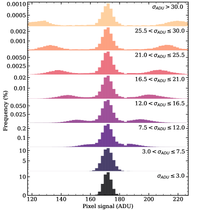
Returning to the standard versus average plot for the sCMOS in Figure 5, the pixels are now grouped in ranges of std. and the signal of each obtained in all of the 21 frames is retrieved. The distribution of each of these groups is shown in the right-hand plot of Figure 5. For pixels showing a temporal deviation of the order of the RON (7.5), the distribution of the measured signal is Gaussian, similar to that of a conventional CCD. The large majority of the pixels are in these first two ranges (45% of the pixels with 3 and 98% with 7.5). For the other ranges (with larger deviations), the pixels begin to show a triple Gaussian distribution, with two smaller peaks that are centered on both sides of the central peak and with similar widths. For larger values of the separation of the peaks is greater. In these anomalous pixels, the pixel distribution is indicative of the following behavior: while most of the time these pixels return values that are around the mean value of the bias level with a normal noise equivalent to readout, their returned values occasionally jump toward larger or smaller values with defined separations and different probabilities for each pixel.
The symmetry in the three Gaussian distributions does not
necessarily mean that all of the anomalous pixels jump between
higher and lower levels with the same probability. In that case,
the standard versus average plot would not show a kite-shaped
scatter but a column, given that the average of the signal would
always lie in the central range. To show a kite-shaped
dispersion, there must be some pixels that tend to exhibit more
deviations toward one of the Gaussians, either the upper or the
lower Gaussian, thus skewing the average to either side and
resulting in the widening of the tails of the mean signal
distribution, which is shown in yellow in the lower left-hand
plot of Figure 3.
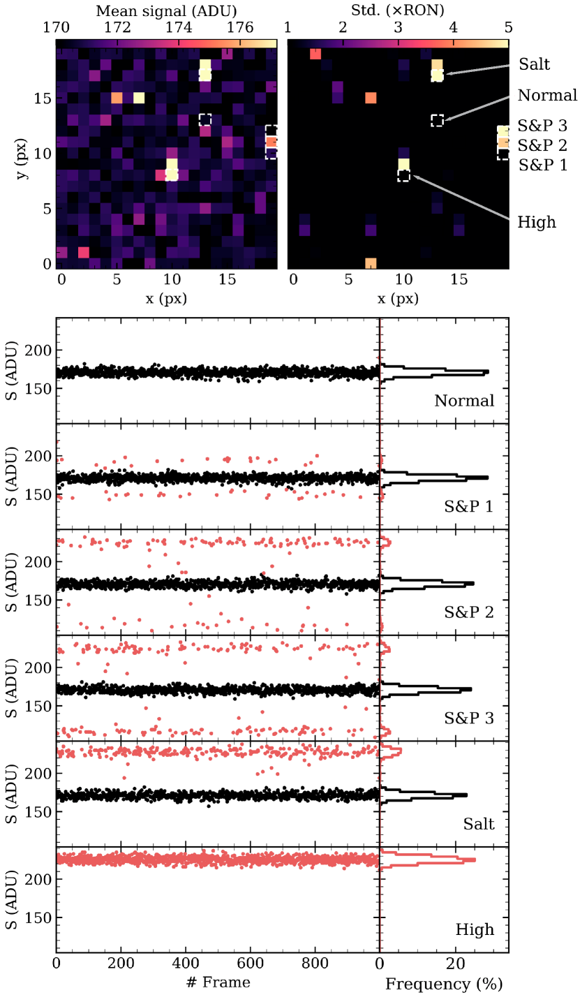
For a more detailed insight into the behavior of these pixels
with high standard deviation, 1000 consecutive bias frames
were obtained with the QHY600M Pro. The temporal average
and standard deviation of all the frames has been taken in a
small central region of , which is shown in the
upper part of Figure 4. Most of the pixels have an average
signal around 171 ADU and a dispersion below the RON, as
expected. However, some of them show anomalous patterns in
the average value, the standard deviation, or both at the same
time. Several pixels have been selected as samples, showing the
time evolution of the signal in the lower plots. As a reference, a
pixel with normal values of average signal and deviation has
been taken, following a normal distribution over the 1000
frames, with mean 170.4 ADU and standard deviation 3.69 ADU. The pixel labeled S&P 1 also has an average signal
similar to the others, with a slightly higher standard deviation
of 6.42 ADU but still close to the RON obtained in the previous
section. However, the temporal distribution reveals how some
points, 5.5% of the total, appear both above and below the
average signal, with a gap of about 20 ADU, which is more
than three times the RON (see the red dots in the plots below).
Other pixels show the same effect more often, e.g., S&P 3, where 19.3% of the 1000 frames show an anomalous value of ADU. This is revealed by a high standard deviation of
23.6 ADU. Although this can be understood as a high RON in
its electronics, it should be noted that its distribution is not a
wide Gaussian but a set of three normal distributions—the main
distribution is centered on 171 ADU, and two smaller ones
corresponding to these random leaps to higher and lower values
at 110 and 230 ADU. The S&P 2 pixel shows jumps at the
same levels but with a higher proportion of values in the upper
level (10.6% of the total) than in the lower level, 3%. Consequently, the signal that was obtained in the average
frame, 174.5 ADU, deviates from the other pixels, as shown in
the image.
These jumps between above- and below-average signal values are observed when blinking between images, regardless of their exposure time and temperature. A pattern of bright and dark pixels that appear and disappear from one frame to the next is observed. This effect, which is sometimes referred as Salt & Pepper, is random telegraph noise (RTN). RTN is the fluctuation of the signal between discrete levels as a consequence of the capture and emission of charges by defects or traps located very close to the Si–SiO2 interface (Uren et al., 1985). In scaled CMOS detectors, this trapping process causes a shift in the relationship between the drain current of the MOS transistor and the gate voltage, discretely increasing or decreasing the offset level, which fluctuates as random trapping and de-trapping of charges, either electrons or holes (Martin-Martinez et al., 2020).
This random noise must be addressed when processing images taken with these detectors. Unusually low or high pixel values can cause deviations in photometric measurements of sources in low light levels. Simply averaging images is not an optimal method because it does not avoid, but may reduce, RTN. For instance, the pixel “Salt” in the Figure 4 shows fluctuations only toward higher, not lower, values, and therefore any averaging that is done by including any of the anomalous points (25.5%) will be inaccurate. The way to deal with these outliers is to take several images and stack them using a more robust statistic. This technique will be discussed further in Section 5. It is also possible to identify some pixels with higher than average signals but with low standard deviation. Some of them are independent of exposure time, such as the pixel “High” in the figure, which can be corrected by subtracting the master bias. However, others depend on exposure time and are treated as warm pixels in the next section.
3.2 Dark current and warm pixels
Dark current (DC) refers to the unwanted leakage current
that is generated in photosensitive devices in the absence of
incoming light, which is mainly due to the thermal generation
of charges in the silicon layer, and is strongly dependent on the
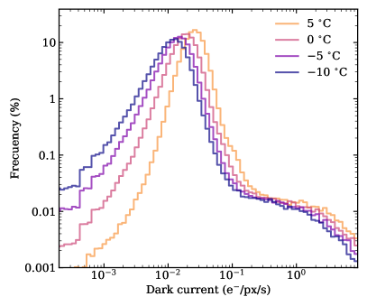
temperature and exposure time. To characterize the DC, five dark frames of 1000 s exposure time were taken, a master bias
taken just before was subtracted, and they were median
stacked. This was done for various temperatures: from C to C on the QHY600M Pro and from C to C on the
QHY411M, on which water cooling was installed for these
tests. The DC distribution in electrons per pixel and seconds of
exposure is shown in Figure 5. The distribution curves have
similar shapes, with a shift toward higher DC with increasing
temperature. When the peak is reached, the DC drops rapidly
toward a smooth hump, from which it drops back down again.
This hump corresponds to a set of pixels with exceptionally
higher DC, which are seen in the images as pixels with a higher
signal that is steady from frame to frame, unlike the Salt &
Pepper effect described in the previous section, which increases
with exposure time. At C, only 0.024% of the QHY600M Pro pixels and 0.005% of the QHY411M have a DC greater
than RON. These warm pixels have signals lower than the
saturation level, and therefore they can be corrected with an
appropriate master dark. The median value of the dark current
for each camera and temperature is shown in Table 2. It is
worth mentioning here that no glow has been seen in any of the
darks taken in either of the cameras, as reported for other
sCMOS sensors (Karpov et al., 2021).
| T (C) | DC (e- px-1 s-1) | |
|---|---|---|
| QHY600M Pro | QHY411M | |
| 5 | 0.025 | |
| 0 | 0.018 | |
| -5 | 0.014 | 0.009 |
| -10 | 0.011 | 0.007 |
| -15 | 0.005 | |
| -20 | 0.004 | |
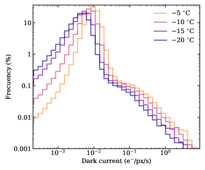
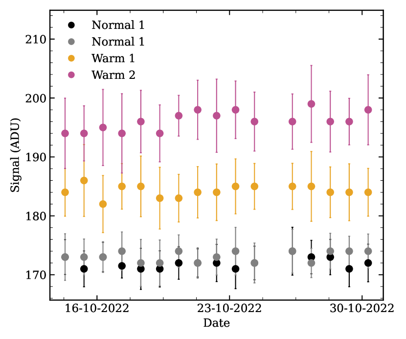
Some warm pixels in a central region of the QHY411M have been identified and revised in more detail. First, sets of 21 dark frames taken consecutively with different exposure times have been stacked. The median signal of two warm and two normal pixels is shown in Figure 6, where the standard deviation is included as uncertainty bars. It is clear that the signal of these warm pixels scales linearly with the exposure time in the range of 1–300 s. The result of the linear least squares fit is shown at the top of the plot, all of them with . Note that in this case a master bias has not been subtracted, and therefore the value of the offset is different from 0. This result implies that it is possible to correct the warm pixels in images of a given exposure time if the slope of this line for each pixel is known, which can be obtained with other exposure times (e.g., at the beginning of the night). Although a scaled master dark is intended to be subtracted from the science images, it should be noted that warm pixels, having a higher thermal signal, will be noisier than those with a lower DC.
For more than 3 weeks, sets of 21 darks of 30 s exposure were taken every night. The median value in these four pixels as a function of time is shown in Figure 7, where the error bars again show their standard deviation. With this test, we have tried to see if there is a substantial variation in the values of these pixels over longer periods of time. Taking into account that the noise in these pixels is a combination of the RON and the thermally generated electrons, which follow a Poissonian distribution, it can be seen that the possible variations in the pixel dark signal over at least these three weeks is not significant with respect to the total noise. Therefore, meaningful night-to-night variations of the master dark or bias are not expected.
3.3 Photon Transfer Curve and linearity
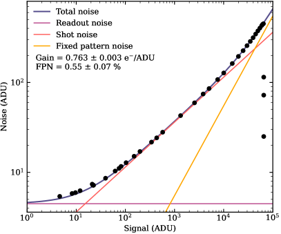
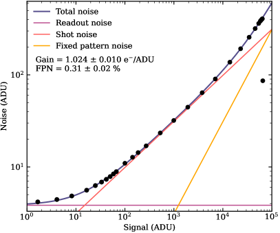
The photon transfer curve (PTC) is used to characterize the response of the sensors to homogeneous illumination, obtaining main features such as the gain—conversion factor between electrons and digital counts (ADU), the full-well capacity (FWC), or the contribution of the different sources to the total noise. The laboratory set-up that is described in Figure 1 was modified by removing the monochromator, so that the light coming from the QTH lamp could directly enter the integrating sphere. The power supply was kept stable. Sets of three images of uniformly illuminated exposures were then taken while increasing the exposure time until the saturation turn-off point was reached. Three bias frames were taken before and after each series, stacked by median 3-clipping and subtracted from all of the illuminated images. A central region of interest (ROI) of unbiased pixels was used for both cameras. The signal was obtained as the mean of the three images stacked. The mean of the standard deviation across the three frames was taken to obtain the noise value.
The total noise under illumination is given by the quadrature sum of three main components: RON, shot noise, and fixed pattern noise (FPN):
| (1) |
where (ADU) is the readout noise, (ADU) the signal, (eADU) the gain and the FPN factor (Janesick, 2007).
The relationship between the noise and signal for the two sensors is shown in Figure 8. The RON was fixed with the value defined in the previous section, while the gain and FPN parameters were obtained by fitting the expression (1) on a logarithmic scale. This procedure was repeated in windows of pixels along the ROI to obtaining a curve for each of them, 360 in total. The rms of the parameter distributions was used to estimate their uncertainty. In both plots, three regions can be distinguished. At low illumination, below 10 ADU, RON, which does not depend on the signal, is the dominating noise source. From then on, shot noise starts to become important, and is essentially the main component between 100 and 10,000 ADU. Thereafter, the contribution of the FPN becomes significant and a deviation from Poissonian behavior is observed. In the QHY600M Pro, this source is the main contributor above 50,000 ADU, with a factor of , being lower, , in the QHY411M, where the shot noise is dominant almost up to the saturation point. A PTC has also been obtained for other operating modes, whose resulting values are included in Table 3.
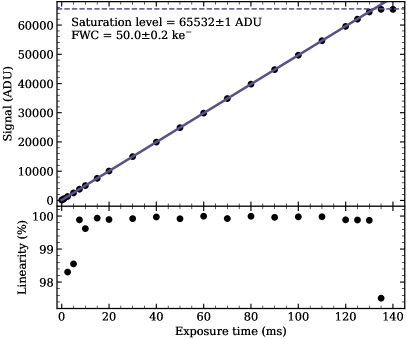
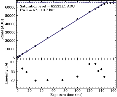
The linearity of the sensors is evaluated by plotting the signal (adding the bias level) against the exposure time, as is done for the standard operating modes in Figure 9. A straight line was fitted to the points between 100 and 60,000 ADU (top plot). The relative rms difference between the points and the line is shown below. In both cases, the deviation from linearity is less than 2% up to the saturation point, which was determined for all of the operating modes and included in Table 3.
| Mode | Gain | RON | FPN | FWC |
| (e-/ADU) | (ADU) | (%) | (ke-) | |
| QHY600M Pro | ||||
| 0@26 | 0.4050.003 | 6.28 | 0.5210.005 | 25.30.2 |
| 1@0 | 0.7630.003 | 4.56 | 0.550.07 | 50.00.2 |
| QHY411M | ||||
| 1@0 | 0.9790.008 | 3.03 | 0.290.02 | 27.20.2 |
| 4@0 | 1.0240.010 | 3.74 | 0.310.02 | 67.10.7 |
| 5@0 | 0.3320.002 | 4.65 | 0.320.02 | 22.80.1 |
| 6@0 | 0.7760.003 | 4.48 | 0.320.02 | 50.60.2 |
| 7@0 | 0.2510.001 | 5.69 | 0.340.02 | 16.500.05 |
3.4 Quantum efficiency
Using the optical setting described in Figure 1, central wavelengths in the range between 350 and 1100 nm with 25 nm steps were selected in the monochromator. The grating configuration was set to have an outcoming light with nm bandwidth. The QHY600M Pro was placed at 13.3 mm from the exit of the dark box, which is separated by 30 mm from the Hamamatsu S2281 photodiode. The total distance between the IMX455 sensor and the photodiode, considering the back focus distance of the camera, was 66.8 mm. In the case of the QHY411M, it could be placed in contact with the box, so the total distance between the photodiode and the IMX411 sensor was 58.5 mm. Both cameras were binned to have enough signal with exposure times shorter than 10 s at those wavelengths where they are less efficient.
Three images were taken at each wavelength step, a master bias that was created at the beginning of the series was subtracted from all of them and they were stacked with the 3-clipped median. Simultaneously, the output intensity of the photodiode placed at the secondary port of the integrating sphere was measured with the picoammeter for approximately 30 s, taking an average value. The observed fluctuations in this value were always less than 2%. The systematic uncertainty of the method is estimated to be around 2%. To avoid vignetting effects at the edges of the dark box-camera junction, a central ROI of binned pixels was used to obtain the median signal , after checking that there were no inhomogeneities in the sensor illumination in that area. The exposure time had to be varied throughout wavelength steps to keep all of the measurements in the shot noise dominated region between 1000 and 40,000 ADUs. The absolute quantum efficiency for each wavelength is given by the expression:
| (2) |
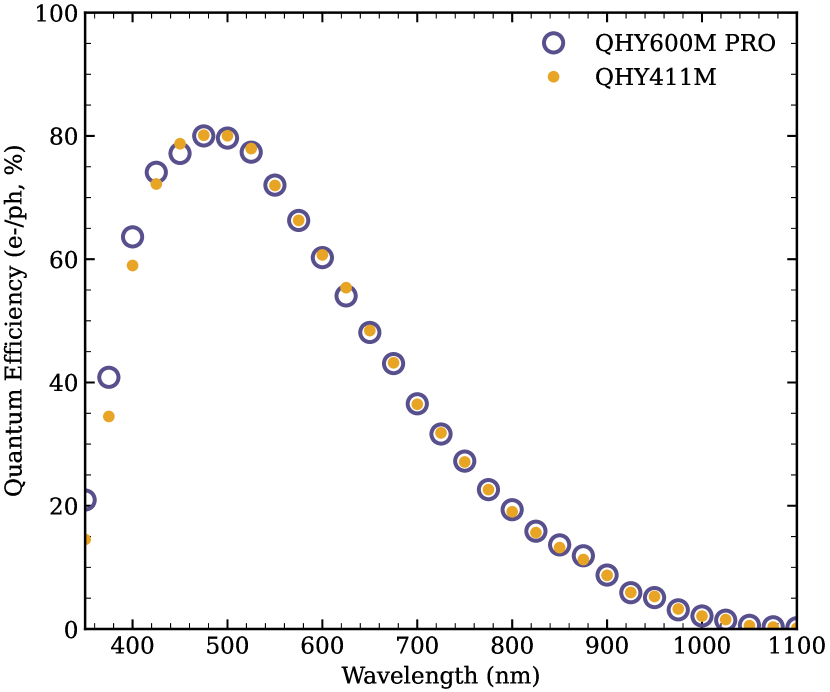
The QE curves for the sensors are shown in Figure 10. Both show very similar behavior, with a peak efficiency of 80% at 475 nm, a steep drop at shorter wavelengths, and a gradual decrease toward the redder ones, with a QE of 40% at 700 nm and 10% at 900 nm. Back-illuminated sCMOS sensors with reduced pixel size, such as the IMX455 and IMX411, have a typical silicon substrate thickness of around 3 m (Yokogawa et al., 2017). This optimizes the photon absorption in the visible range but makes the less energetic photons, which have a higher penetration capability, less likely to be detected. Without any additional red enhancement technology, improving efficiency in the red and near-infrared requires a thicker substrate that, with such small pixels, would lead to image degradation owing to crosstalk between adjacent pixels. This is the reason for the poor performance at longer wavelengths.
It should be noted that the curves that are obtained here represent an overall reduction of 9% over the full absolute QE curve published by QHYCCD, which has a peak of 92% at 450 nm, 46% at 700 nm, and 15% at 900 nm. Nonetheless, the conditions and configuration used by them, as well as the uncertainties in their measurements, are unknown and the calibration method to obtain the QE curves is different from the one used here, which has been used to calibrate multiple astronomical instruments before. The same procedure and test bench have been used, for instance, to calculate the QE in sCMOS cameras such as Andor Marana, FLI-Kepler, and ORCA-Hamamatsu. They have also been used in several deep depletion CCDs, such as the well-known Teledyne e2v 4482 and 231-84 BI. In all cases, QE fits rather well with data supplied by the manufacturers. Gill et al. (2022) have very recently presented a low-cost method to obtain, among other features, the absolute QE of detectors being applied to the IMX455 sensor. Their results also show a lower performance than that presented by QHYCCD, especially in the red part, although they had a similar peak efficiency, with 93% at 480 nm, 42% at 700 nm, and 10% at 900 nm, making an overall deviation from our results of 5%. Finally, Betoule et al. (2023) have studied the quantum efficiency of the IMX411 sensor in great detail and obtained a result that is very similar to Figure 10, with a peak of 83% at 490 nm, 37% at 700 nm and 6% at 900 nm.
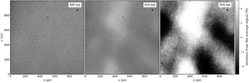
During the tests, optical etaloning was observed at longer wavelengths, as shown in Figure 11 for the QHY600M Pro. Similar behavior was observed also for the QHY411M and reported by Betoule et al. (2023). The maximum variation over the average frame mean value is around 1% at 650 nm, and reaches 10% at 850 nm and above. This is a known effect in thinned back-illuminated devices, resulting from multiple reflections produced inside the depletion region by a mismatch between its refractive indices and the adjacent layers. This effect has not been observed in sky images taken with TAR04 using a wider bandwidth, such as SDSS i′ (690–850 nm).
3.5 Charge persistence
Charge persistence is an effect that occurs when a portion of the signal remains in the detector element after the sensor has been read out. It is a consequence of the creation of traps at the interface between the photodiode and the transfer gates, which capture free electrons and gradually release them, resulting in a decay of the residual signal in the subsequent images after the illuminating source has been removed. This effect has been observed with tests performed in the laboratory with the FLI Kepler KL400 and Andor Marana cameras, both with GSENSE400BSI sensors, showing a behavior similar to that reported by Karpov et al. (2021). Although they did not observe any effect in sky images, previous tests performed with these cameras on the same telescopes used in our work did show a smearing effect in pixels that had previously been exposed close to the FWC, which remained visible up to tens of minutes later.
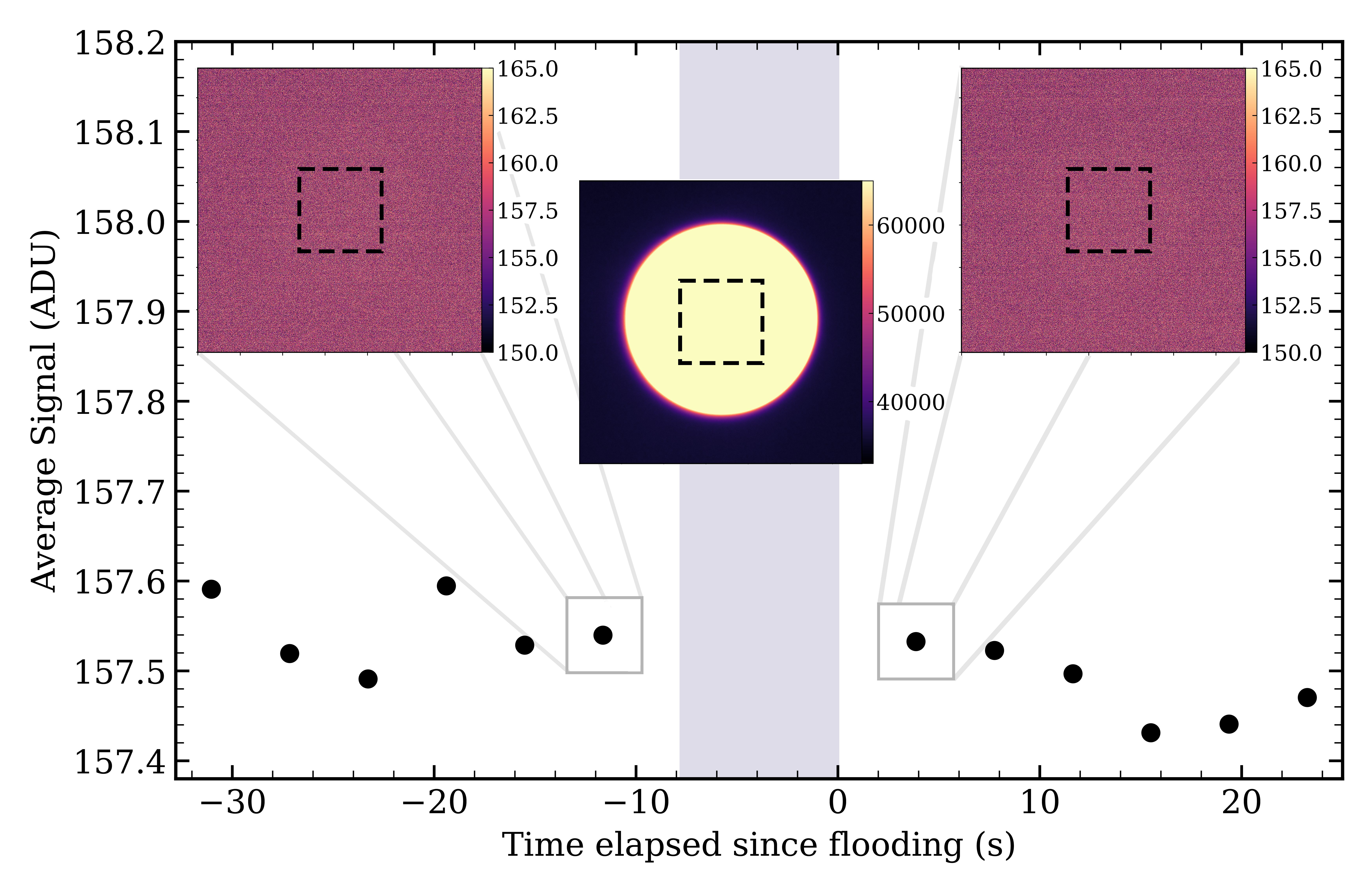
This effect has been tested in the laboratory for both sensors. To do so, following the same set-up used in Section §3.3, i.e., removing the monochromator and exposing the cameras to the QTH lamp light, a pinhole was placed inside the black box, just in front of the sensor. Consecutive 1 s images were taken with the shutter closed. The shutter was then opened for about 10 s, saturating the illuminated pixels, and closed again. This sequence is shown in Figure 12. On the top are the images taken with the QHY600M Pro before the shutter was opened (left-hand), during the exposure to the light coming from the pinhole (center), and just after the shutter was closed again (right-hand). In the central region of the illuminated spot area, indicated by a dashed square, the mean signal has been measured and is shown in black dots below. The signal before and after the flooding shows a stable trend, with very small oscillations, not a sharp increase in the signal right after the exposition followed by a slow decay to the original level, as shown in Figure 10 of Karpov et al. (2021). Hence, we conclude that the IMX455M and IMX411M sensors do not exhibit charge persistence.
4 On-sky tests
Both cameras have been extensively tested on images taken
with telescopes, obtaining photometric accuracies as expected
for the characteristics described above. The QHY600M Pro
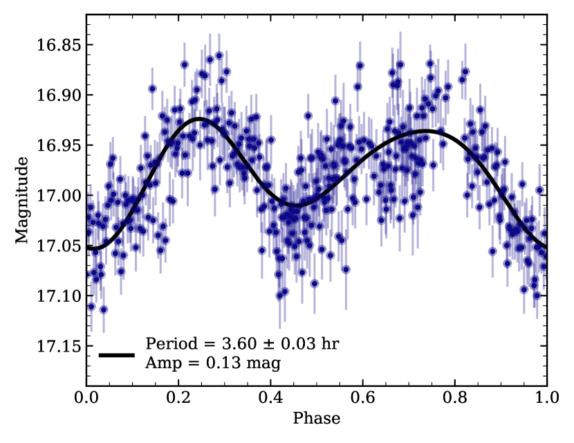
was installed at the prime focus of a 0.46-m /2.2 telescope. Figure 13 shows the phased light curve of asteroid (3200)
Phaethon, which was observed for 6 consecutive hours. At the time of observation, the object had an apparent magnitude of
and was moving at a speed of 1′′.6 minute. The
photometric uncertainties that we obtained are in the order of
hundredths of a magnitude and the rotation of the asteroid, with
an amplitude of 0.13 mag, is clearly detectable. This camera is
a very suitable choice for very fast telescopes with primary
focus because its small size and compact shape drastically
reduce obscuration. With a pixel size of 3.76 m, it also allows
us to obtain a plate scale that is very suitable for sites with
excellent seeing, such as the Teide Observatory. Furthermore,
given its low readout noise and negligible readout time, it is
possible to take continuous short frames and combine them by
aligning with the object or the stars, thus allowing fainter
objects to be reached with very little time lost. This also allows
the study of, for instance, very fast rotating objects with good
temporal sampling (Licandro et al., 2023b) or using “shift-and-add”
techniques, such as synthetic tracking (Shao et al., 2014), to improve the detection performance of faint fast-moving
objects.
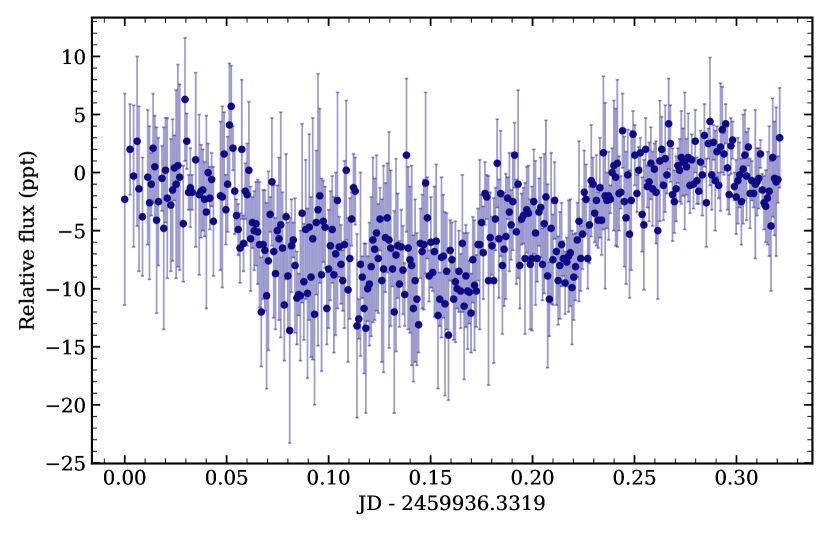
Figure 14 shows a transit of the exoplanet TOI-1135 that was observed with the QHY411M mounted on one of the Nasmyth foci of the TTT-2 telescope, 0.80-m /6.85, SDSS g′ filter, with a plate scale of 0′′.14 px-1. Groups of four images of 5 s exposure were stacked to improve the SNR. The standard deviation of the differential aperture photometry measurements in pre-transit, during, and post-transit is 2.2, 3.3, and 2.0 mmag, respectively (M. Mallorquin et al., in preparation). With such a small plate scale, the psf was oversampled, with approximately 8 px of FWHM, spreading the flux of the star over a larger number of pixels. For very bright targets, such as this mag star, this allows slightly longer exposures to be taken without reaching the saturation point, thus reducing the random and flat-fielding errors of the telescope that, with a larger scale, would perhaps need some defocusing (Southworth et al., 2009). In addition, by taking short exposures, the time lost on a CCD could be equivalent to, or even longer than, the exposure time, which makes it very inefficient. With the QHY411M, the exposure time could be extended, thus improving photometric accuracy, and the readout time is almost non-existent. Although such small plate scales are generally undesirable, they allow these cameras to be used in other scientific applications (e.g., fast-moving object astrometry or lucky imaging).
5 Discussion
The two instruments with sCMOS sensors that are analyzed here present characteristics that are compatible with their use in astronomy: they are linear over the whole dynamic range, have a high full-well capacity, and are slightly affected by dark current, despite being able to work at higher temperatures than CCDs. Regarding the quantum efficiency, although the curve obtained here is slightly lower than that reported by the manufacturer, 80% at 500 nm is an acceptable performance for many scientific programmes and is in general similar or better than other CCD sensors in the same cost range. An improvement in efficiency toward redder wavelengths should be achieved in the next few years, so that sCMOS sensors can be used on a wider variety of observational targets.
The small pixel size means that these sensors are generally not the best solution for slow focal length systems, except for dedicated programmes such as high spatial resolution or lucky imaging. Binning in sCMOS sensors is done after exposure, so it does not improve the readout noise or frame rate. In general, in case it is needed, it is better to do this by software after the exposure, so that the statistics can be preserved and the 16 bit limit is not reached. Nevertheless, they can be very valuable in fast telescopes with larger fields and higher plate scales, which allows better sampling of the PSF. In addition, their manageability, and small size and weight are very interesting, e.g., for prime focus telescopes.
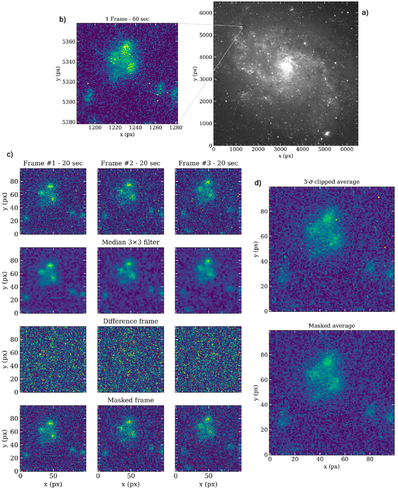
The S&P effect is one of the main issues that affect the use of these IMX455 and IMX411 sensors for photometric measurements. Figure 15(a) shows an image of the galaxy M33 taken with the QHY411M on the TAR04 telescope, with a UV/IR-Cut/L filter, in a single exposure of 60 s. When zooming in on a small area of 100100 pixels (b), several pixels are observed with values that are clearly higher than those of their neighbors, as described in Section 3.1. This effect could influence the photometry of faint objects because the amplitude of this random fluctuation may be comparable to the source signal in the pixel.
SSeveral strategies can be pursued to mitigate this problem, especially by using several consecutive frames. Figure 15(c) shows a sequence of s, where the S&P is clearly visible in each of them. If simple averaging were performed, then the outliers would skew the signal obtained. Algorithms such as 3 clipping that use outlier-sensitive dispersion measures generally do not work either because these metrics are biased by these fluctuations and define a very wide clipping range. This is seen in Figure 15(d) (top plot), where the three frames have been combined with an average after 3-clipping. Some of the pixels that exhibited S&P also show deviating values in the stacked frame.
It is common to use spatial filters for this kind of localized
noise. The most typical for S&P is a median filter, where the
value of each pixel is replaced by the median of the values of
this and its close neighbors. This is done in the second row of
Figure 15(c). Note that the image has been smoothed and the
anomalous pixels may have disappeared. However, this has
been done at the expense of: (1) changing the signal and noise pattern of the image and (2) correlating the nearby pixels.
Although this is a very useful filter for improving the cosmetics
of the images, the photometry measurement in the resulting
image may be highly biased because the fluxes of each pixel
have been altered by its neighbors.
In this work, a solution based on convolutions and these two previous ideas is proposed to try to mitigate the S&P effect. First, it should be considered that the S&P effect mostly impacts low noise areas, such as the sky background or faint sources. For bright sources, the shot noise becomes higher than the random telegraph noise and dominates all of the other fluctuations. The median filter can be used to obtain a reference frame to identify outliers because, in well-sampled fields, they are a good approximation to a smoothed frame. This can be seen in Figure 15(c), where the third row shows the difference between the raw frame and the one filtered with a median kernel. The residual pattern is generally homogeneous, both in the sky area and in the vicinity of the sources. To identify the S&P, a threshold of 12 ADU has been set because it is at this point that the distribution of three Gaussians in Figure 3 (right-hand) starts to be revealed. Hence, all of the pixels whose absolute difference between the raw value and that resulting from the convolution with the median filter is greater than 12 ADU are masked. In the bottom row of Figure 15(c), the raw frames are shown with the pixels masked in red. By having a sequence of frames, the average of the unmasked values of each pixel can be taken to get a stacked image, which is shown on the bottom right-hand of the figure, where the S&P contamination has been highly reduced. In cases where a pixel shows S&P in all of the frames of the sequence and is therefore masked, the astronomer has to decide, for instance, either not to take that pixel into account in the photometry or to replace its value by an approximation, such as an interpolation of the neighboring pixels or their median. In the example included here, this happens in only two pixels out of . It should be noted that this method may be less accurate in fields with critically sampled sources. A further review is currently underway for future work.
Developing new algorithms or even using those already available in common packages such as IRAF (Tody, 1986) or Astropy (Astropy Collaboration et al., 2013) may not be trivial when working with these cameras. The size of the raw 16 bit images of the QHY600M Pro are about 120 MB, while those of the QHY411M are 300 MB. If a sequence is taken at a high frame rate, then the data set may not be manageable with commonly available CPU capacities. The advantage of convolution-based approaches and simple arithmetical operations, such as median filtering or frame differencing, is that they are easily deployable on GPUs, which allows the data to be processed more efficiently and faster. The development of GPU algorithms for astronomical image processing is essential for further progress in the use of large sensors, such as these sCMOS.
6 Conclusion
In the previous sections, the key features of the QHY600M Pro and QHY411M cameras as scientific instruments have been discussed in detail. For astronomy, they have characteristics that make them very suitable for general use, although certain issues need to be addressed. Our main conclusions are that:
-
1.
The built-in electronics in the pixels of sCMOS sensors require that each pixel should be considered as an individual detector and this should be taken into account when performing processes such as bias or dark subtraction. Spatial inhomogeneities in darkness are detectable all over the frame.
-
2.
Their dark current is very low, as is the number of warm pixels. They are stable for at least several weeks and their signal scales linearly with exposure time, so they may be quite easily removed with dark subtraction. This is an improvement from previous sCMOS sensors and makes it possible to take images with longer exposure times without being affected by dark current.
-
3.
Its quantum efficiency peaks at 80% at 475 nm and then drops rapidly at longer wavelengths, with 40% at 700 nm and 10% at 900 nm.
-
4.
They do not exhibit charge persistence or edge glow.
-
5.
These sensors are affected by random telegraph noise, which can introduce non-negligible deviations in photometric measurements of low-brightness sources. Simple frame averaging, even with algorithms such as -clipping, is not enough to mitigate its effect.
-
6.
They show promising performance on photometric observations done with both fast and slow telescopes.
Their low cost, power consumption, and replicability make
both cameras a very suitable solution for astronomical
applications, especially with regard to their high frame range,
near-zero readout time, and low readout noise. These sensors
are very good options for fast small telescopes with large fields
because of their small pixel size and large formats. The
combination of such telescopes and cameras permit very large
field-of-view images with plate scales with reasonably good
sampling of the PSF. For instance, a 11′′ /2.2 telescope such as
the Celestron RASA11 with a QHY600 camera can produce
images covering a FOV of 7.5 deg2 with a plate scale of 1′′.27 px-1, which are excellent options for surveys such as
ATLAS-Teide (Licandro et al., 2023a). Even so, having the
necessary computational tools to process the data, especially
GPU developments, is essential to take advantage of the full
performance of these cameras.
The authors declare no conflict of interest or relationship with the manufacturers of the cameras tested. M.R.A, M.S-R and J.L. acknowledge support from the ACIISI, Consejería de Economía, Conocimiento y Empleo del Gobierno de Canarias and the European Regional Development Fund (ERDF) under grant with reference ProID2021010134 and from the Agencia Estatal de Investigacion del Ministerio de Ciencia e Ińnovacion (AEI-MCINN) under grant ”Hydrated Minerals and Organic Compounds in Primitive Asteroids” with reference PID2020-120464GB-100. This research has been partially funded by Light Bridges, SL. which provided the QHY411M and Andor iKon-L 936 cameras for the tests presented here. This article includes observations made in the Two meter Twin Telescope (TTT) at the IAC’s Teide Observatory that Light Bridges, SL, operates on the Island of Tenerife, Canary Islands (Spain).
References
- Astropy Collaboration et al. (2013) Astropy Collaboration, Robitaille, T. P., Tollerud, E. J., et al. 2013, A&A, 558, A33, doi: 10.1051/0004-6361/201322068
- Betoule et al. (2023) Betoule, M., Antier, S., Bertin, E., et al. 2023, A&A, 670, A119, doi: 10.1051/0004-6361/202244973
- Bigas et al. (2006) Bigas, M., Cabruja, E., Forest, J., & Salvi, J. 2006, Microelectronics J., 37, 433, doi: https://doi.org/10.1016/j.mejo.2005.07.002
- Boyle & Smith (1970) Boyle, W. S., & Smith, G. E. 1970, Bell Syst. Tech. J., 49, 587, doi: 10.1002/j.1538-7305.1970.tb01790.x
- Coates et al. (2009) Coates, C., Fowler, B., & Holts, G. 2009, White Paper: Scientific CMOS technology, a high-performance imaging breakthrough, Available at: https://www.pco.de/fileadmin/user_upload/db/download/scmos_white_paper_2mb.pdf (accessed Oct 3, 2022)
- Fossum (1997) Fossum, E. R. 1997, Nucl. Instrum. Methods Phys. Res. A, 395, 291, doi: 10.1016/S0168-9002(97)00812-7
- Gill et al. (2022) Gill, A. S., Shaaban, M. M., Tohuvavohu, A., et al. 2022, in Society of Photo-Optical Instrumentation Engineers (SPIE) Conference Series, Vol. 12191, X-Ray, Optical, and Infrared Detectors for Astronomy X, ed. A. D. Holland & J. Beletic, 1219114, doi: 10.1117/12.2627564
- Janesick (2007) Janesick, J. R. 2007, Photon Transfer DN → (Bellingham, WA: SPIE Press)
- Janesick et al. (1987) Janesick, J. R., Elliott, T., Collins, S., Blouke, M. M., & Freeman, J. 1987, Optical Engineering, 26, 692, doi: 10.1117/12.7974139
- Karpov et al. (2021) Karpov, S., Bajat, A., Christov, A., Prouza, M., & Beskin, G. 2021, arXiv e-prints, arXiv:2101.01517. https://arxiv.org/abs/2101.01517
- Law et al. (2022) Law, N. M., Corbett, H., Galliher, N. W., et al. 2022, PASP, 134, 035003, doi: 10.1088/1538-3873/ac4811
- Licandro et al. (2023a) Licandro, J., Tonry, J., Alarcon, M. R., Serra-Ricart, M., & Denneau, L. 2023a, arXiv e-prints, arXiv:2302.07954, doi: 10.48550/arXiv.2302.07954
- Licandro et al. (2023b) Licandro, J., Popescu, M., Tatsumi, E., et al. 2023b, MNRAS, 521, 3784, doi: 10.1093/mnras/stad708
- Martin-Martinez et al. (2020) Martin-Martinez, J., Rodriguez, R., & Nafria, M. 2020, Advanced characterization and analysis of random telegraph noise in CMOS devices (Springer), 467–493
- Ofek et al. (2023) Ofek, E. O., Ben-Ami, S., Polishook, D., et al. 2023, arXiv e-prints, arXiv:2304.04796, doi: 10.48550/arXiv.2304.04796
- Princeton Instruments (2016) Princeton Instruments. 2016, New Scientific CMOS Cameras with Back-Illuminated Technology. Technical Note., Available at: https://www.princetoninstruments.com/wp-content/uploads/2020/11/TechNote_sCMOSBackIlluminatedTech.pdf (accessed July 8, 2022)
- Qiu et al. (2013) Qiu, P., Mao, Y.-N., Lu, X.-M., Xiang, E., & Jiang, X.-J. 2013, Research in Astronomy and Astrophysics, 13, 615, doi: 10.1088/1674-4527/13/5/012
- Qiu et al. (2021) Qiu, P., Zhao, Y., Zheng, J., Wang, J.-F., & Jiang, X.-J. 2021, RAA, 21, 268, doi: 10.1088/1674-4527/21/10/268
- Schildknecht et al. (2013) Schildknecht, T., Hinze, A., Schlatter, P., et al. 2013, in Proceedings of 6th European Conference on Space Debris, Darmstadt, Germany
- Shao et al. (2014) Shao, M., Nemati, B., Zhai, C., et al. 2014, ApJ, 782, 1, doi: 10.1088/0004-637X/782/1/1
- Southworth et al. (2009) Southworth, J., Hinse, T. C., Jørgensen, U. G., et al. 2009, MNRAS, 396, 1023, doi: 10.1111/j.1365-2966.2009.14767.x
- Tody (1986) Tody, D. 1986, in Society of Photo-Optical Instrumentation Engineers (SPIE) Conference Series, Vol. 627, Instrumentation in astronomy VI, ed. D. L. Crawford, 733, doi: 10.1117/12.968154
- Tonry et al. (2018) Tonry, J. L., Denneau, L., Heinze, A. N., et al. 2018, PASP, 130, 064505, doi: 10.1088/1538-3873/aabadf
- Uren et al. (1985) Uren, M., Day, D., & Kirton, M. 1985, Applied physics letters, 47, 1195
- Yokogawa et al. (2017) Yokogawa, S., Oshiyama, I., Ikeda, H., et al. 2017, Scientific Reports, 7, 3832, doi: 10.1038/s41598-017-04200-y