The out-of-plane magnetoresistance in a Van der Waals thin film of WTe2
Abstract
We report the magneto-transport measurements of thin film devices of the topological Weyl semimetal WTe2 with the applied current along and vertical to the in-plane directions. The device is composed of a Van der Waals thin film of WTe2 sandwiched between top and bottom Au electrodes. At low temperatures, we found a large unsaturated in-plane magnetoresistance and a saturated out-of-plane magnetoresistance when the external magnetic fields are applied perpendicular to the plane. By analysis of Shubnikov-de Haas oscillations, one oscillation peak is found in the out-of-plane magnetoresistance, in contrast to four oscillation peaks in the in-plane magnetoresistance. Our work provides new insight into the origin of the unsaturated magnetoresistance in WTe2 and may inspire non-planar engineering to reach higher integration in spintronics.
I introduction
WTe2 is a layered transition-metal dichalcogenide (TMD) consisting of a tungsten layer surrounded by two tellurium layers stacked along the axis. It exhibits an extremely large magnetoresistance (XMR) and shows no sign of saturation in high fields.Ali et al. (2014) The XMR in the type-II Weyl semimetal WTe2 recently stimulates extensive theoretical and experimental magneto-transport investigations.Cai et al. (2015); Zhu et al. (2015); Thoutam et al. (2015); Li et al. (2017); Pletikosić et al. (2014) ARPES experiment in WTe2 suggests that the XMR is attributed to the compensation between the balanced electron and hole populations,Pletikosić et al. (2014) like the behaviour expected in a perfectly-compensated semimetal.Pippard (1989) In contrast to the normal semimetal, WTe2 is a type-II Weyl semimeta, where Fermi surfaces consist of a pair of electron- and hole- pockets contacting at the Weyl node.Soluyanov et al. (2015); Li et al. (2017) Shubnikov-de Haas effect (SdH) oscillations, Seebeck and Nernst measurements support the Fermi surface consisting of two pairs of electron-like and hole-like pocketsZhu et al. (2015); Cai et al. (2015).
With the reduction of thickness, a metal-to-insulator transition is observed in thin WTe2 flakes.Wang et al. (2015) Gate-tunable magnetoresistance is found in ultra-thin WTe2.Wang et al. (2016); Liu et al. (2017) In atomically thin WTe2, the magnetoresistance can be tuned from positive to negative.Zhang et al. (2017) In addition, by electrostatically doping ultra-thin WTe2, the XMR is turned on and off.Fatemi et al. (2017) In a monolayer crystal WTe2, the quantum spin Hall effectWu et al. (2018) and Landau quantizationWang et al. (2021) are observed. In bilayers of WTe2, the nonlinear Hall effect is observed in spite of its non-magnetic and time-reversal-symmetric conditions.Ma et al. (2019) It needs further investigation in the WTe2 ultrathin flake, where the electronic structure is modulated by the dimension.Xiang et al. (2018)
In this paper, we fabricate a thin film device of WTe2 with top and bottom electrode structure. By choosing the current directions, we performed in-plane and out-of-plane magneto-transport measurements in this device. We found a large unsaturated in-plane magnetoresistance and a saturated out-of-plane magnetoresistance. The Shubnikov-de Haas oscillations are also observed in the magnetoresistance at both directions at low temperature. By analysis of the oscillations, we found four oscillation peaks in the in-plane magnetoresistance, but one oscillation peak in the out-of-plane magnetoresistance.
II Experimental details
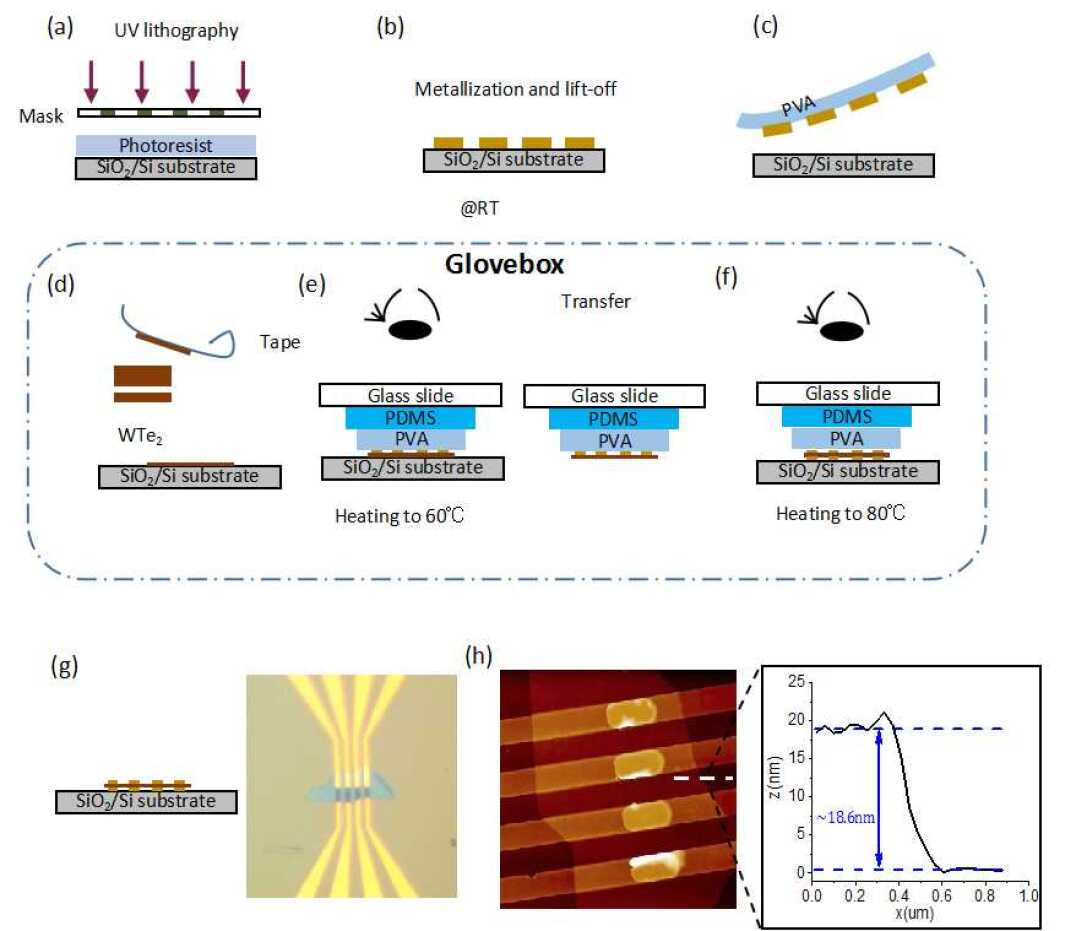
Single crystals of WTe2 were synthesized using a self-flux method. WTe2 thin flake was transferred with the polyvinyl alcohol (PVA), based on our previous technique.Zhang et al. (2021) Fig. 1 shows the schematics of the vertical contact fabrication and assembly process comprised of the following steps: (a) The electrodes are patterned when the mask is exposed to UV light. (b) Gold is deposited to the SiO2/Si substrate and the residual photoresist is removed with a standard lift-off process as depicted. (c) PVA solution was spin-coated on the SiO2/Si substrate with Au electrodes at a speed of 4000 rpm. It created a PVA film of about 900 nm. After 12 h in atmosphere, the PVA becomes dry and solid. At room temperature, the Au electrodes are gently peeled off from the SiO2/Si substrate by PVACao et al. (2020); Zhang et al. (2021). (d) The WTe2 thin flakes can be exfoliated using scotch tapes and attached to SiO2/Si substrate prior to plasma cleaning. (e) A piece of the Au/PVA strip is attached to PDMS and glass slide, under the microscope, they are aligned to the thin sample flake. After a short baking of 60oC, the sample can be gently separated from the substrate and grabbed by the PVA side. (f) We align the Au electrodes part on the SiO2/Si substrate with the WTe2/Au/PVA/PDMS part on the glass slide under the microscope. After a short baking of 80oC, the top PDMS is detached. (g) After the PVA is washed away in deionized water and the part left is a Au/WTe2/Au vertical structure on the SiO2/Si substrate. The optical microscope image of the vertical device is shown in the right part. Atomic force microscopy (AFM), Fig. 1(h), reveals the vertical channel region (in bright yellow colour) of the device. The width of the vertical channel is about 6 m, the height profile in the inset shows that the thickness of the WTe2 flake is 18.6 nm.
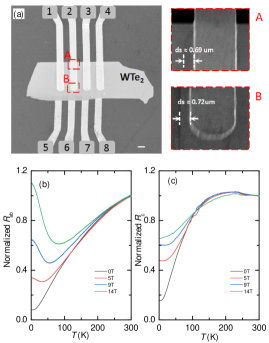
Fig. 2(a) shows the scanning electron micrograph (SEM) of the WTe2 Van der Waals device. The thin flake of WTe2 is sandwiched between Au electrodes. The top and bottom Au electrodes are laterally edge-to-edge separated by 3 m from each other, respectively. The mismatch among top and bottom electrodes is inspected by the magnified area in the inset. The mismatch length (ds) is about 0.69 m and 0.72 m, with a small inclination of about 4.3. The device can be used for measuring the planar and vertical transport properties at the same sample. For the in-plane transport configuration, the electrodes 5 and 8 are used as current probes and inner electrodes 6 and 7 are connected to a voltmeter. While for out-of-plane transport configuration, the electrodes 2 and 6 are used as current probes and the electrodes 3 and 7 as voltage probes. The resistivity was measured by two sets of lock-in amplifiers Stanford SR830 in a 14 T Oxford instrument Teslatron PT. To avoid the influence of noise from different directions, the out-of-plane transport measurements are performed subsequently after the in-plane measurements.
III Results and discussions
Fig. 2(b) and 2(c) show the temperature () dependence of the normalized resistances ( and ) at the same WTe2 sample under the external magnetic fields applied perpendicular to the plane and the applied current () along the in-plane and the out-of-plane directions, respectively. It is found that the at 0 T decreases monotonically from room temperature as the temperature cools down, yielding a residual resistivity ratio (RRR) about 12.5 in Fig. 2(b).The shows a remarkable increase after reaching a minimum at the turn-on temperature, when a magnetic field is applied. The turn-on temperature is found to be shifted to a higher temperature as increasing at the investigated magnetic field range. On the other hand, the RRR for at 0 T is about 6.4 (Fig. 2(c)), which is less than the one for . Furthermore, the show a negligible increase at low temperature at the investigated T. It thereby suggests that the in-plane and out-of-plane transport have distinct electronic properties.
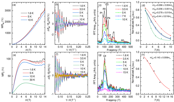
Fig. 3(a) shows the dependence of the in-plane magnetoresistance (MRab) at various temperatures (). The MRab increases with without a sign of saturation, consistent with the literature.Ali et al. (2014); Kong et al. (2015); Zhu et al. (2015); Zhao et al. (2015); Xiang et al. (2015) At high , the Shubnikov-de Haas quantum oscillations are observed in all the temperatures from 1.6 K to 10 K. The oscillatory component can be extracted by subtracting a second-order polynomial background over the MR. The (H) as a function of is plotted in Fig. 3(b). Fast Fourier transformation (FFT) has been performed and the amplitude spectra are illustrated in Fig. 3(c). The frequencies of the thin flake show four major peaks at 77.8, 100, 133, and 161 T, originated from two pairs of electrons and hole pockets.Zhu et al. (2015); Li et al. (2017); Cai et al. (2015) The decrease and shift of the SdH oscillation frequencies are due to the spatial confinement contributing to the electronic structure in thin samplesXiang et al. (2018); Li et al. (2017). In addition to the four distinct frequencies, a fifth frequency(P5= 254 T) is detected. It is externally caused by the magnetic breakdown as suggested by a previous study.Zhu et al. (2015); Cai et al. (2015) The peaks correspond to the orthogonal cross-sectional area of the Fermi surface(FS) , as described by the Onsager relation =(/2), where is the flux quantum. The effective cyclotron mass of carriers at the observed Fermi surface sheets is evaluated from the temperature dependence of normalized FFT amplitude using the the Lifshitza-Kosevich (LK) formula.
where and is the effective mass. Normalized FFT amplitudes of the four peaks for the MRab as a function of are plotted in Figs. 3(d). Their effective masses are estimated to be 0.266 , 0.206 , 0.278 , 0.446 for oscillation peaks P1, P2, P3, P4, respectively.
When the current is applied through the vertical channel, we can probe the c-axis magnetoresistance transport properties in one single sample. The dependences of MRc under different are shown in Fig. 3(e). The MRc at 1.6 K increases with and saturates at large magnetic field, which is different with MRab of WTe2. The MRc shows oscillations at the temperature range from 1.6 K to 15 K, but then disappear at higher temperatures. Similar to the MRab, the oscillatory component of MRc is obtained after a background subtraction, and (H) is periodic with as shown in Fig. 3(f). One sharp peak Q1 = 106 T is obtained for the MRc in Fig. 3(g). After a fitting with the normalized amplitude Ac, the effective mass is estimated to be 0.143 me (Fig. 3(h)), smaller than those obtained from the in-plane direction transport measurements. Since the oscillation peaks and effective mass are related to the Fermi surface, the Fermi surface obtained from in-plane transport is different from the out-of-plane transport. Thus the presence of different behaviours of MRab is determined by the Fermi surface that can be modified by the applied current directions.
In addition to the in-plane oscillation, we discover the quantum oscillation in the out-of-plane magnetoresistance. One possible interpretation would be that the Fermi arcs on the top and the bottom surface contribute to a novel type of quantum oscillation phenomena.Potter et al. (2014) However, the underlying origin needs further experimental evidence and theoretical analysis. In bulk WTe2, the resistivity first increases with magnetic field at low magnetic field before it starts oscillating with suppressing out-of-plane magnetoresistanceBi et al. (2018). There is no previous report for out-of-plane magnetoresistance in WTe2 thin films. The appearance of oscillation at a damping magnetoresistance in the ultrathin film is consistent with the bulk.
IV Summary
In summary, we introduced the fabrication of the vertically assembled Au/WTe2/Au/device and characterize its out-of-plane and in-plane transport properties. A saturated out-of-plane magnetoresistance is observed at low temperatures while it remains unsaturated for the in-plane magneto-transport. There are quantum oscillations discovered in the out-of-plane transport in addition to the in-plane transport. A single peak in the out-of-plane direction oscillation is found. Our results suggest that the presence of different behaviours of magnetoresistance and the topology of Fermi surfaces of WTe2 could be determined by applied current directions.
Acknowledgements.
T.H. acknowledge the support of NSFC Grant No. 11574338. H.X. acknowledge the support of NSAF Grant No. U1530402. Y.G. Shi acknowledge the support of NSFC Grant No. U2032204 and the Informatization Plan of Chinese Academy of Sciences(CAS-WX2021SF-0102).∗ liuys@baqis.ac.cn † c.m.schneider@fz-juelich.de
References
- Ali et al. (2014) M. N. Ali, J. Xiong, S. Flynn, J. Tao, Q. D. Gibson, L. M. Schoop, T. Liang, N. Haldolaarachchige, M. Hirschberger, N. P. Ong, et al., Nature 514, 205 (2014).
- Cai et al. (2015) P. Cai, J. Hu, L. He, J. Pan, X. Hong, Z. Zhang, J. Zhang, J. Wei, Z. Mao, and S. Li, Physical review letters 115, 057202 (2015).
- Zhu et al. (2015) Z. Zhu, X. Lin, J. Liu, B. Fauqué, Q. Tao, C. Yang, Y. Shi, and K. Behnia, Physical review letters 114, 176601 (2015).
- Thoutam et al. (2015) L. Thoutam, Y. Wang, Z. Xiao, S. Das, A. Luican-Mayer, R. Divan, G. Crabtree, and W. Kwok, Physical review letters 115, 046602 (2015).
- Li et al. (2017) P. Li, Y. Wen, X. He, Q. Zhang, C. Xia, Z.-M. Yu, S. A. Yang, Z. Zhu, H. N. Alshareef, and X.-X. Zhang, Nature communications 8, 1 (2017).
- Pletikosić et al. (2014) I. Pletikosić, M. N. Ali, A. Fedorov, R. J. Cava, and T. Valla, Physical review letters 113, 216601 (2014).
- Pippard (1989) A. B. Pippard, Magnetoresistance in metals, Vol. 2 (Cambridge university press, 1989).
- Soluyanov et al. (2015) A. A. Soluyanov, D. Gresch, Z. Wang, Q. Wu, M. Troyer, X. Dai, and B. A. Bernevig, Nature 527, 495 (2015).
- Wang et al. (2015) L. Wang, I. Gutiérrez-Lezama, C. Barreteau, N. Ubrig, E. Giannini, and A. F. Morpurgo, Nature communications 6, 1 (2015).
- Wang et al. (2016) Y. Wang, E. Liu, H. Liu, Y. Pan, L. Zhang, J. Zeng, Y. Fu, M. Wang, K. Xu, Z. Huang, et al., Nature communications 7, 1 (2016).
- Liu et al. (2017) X. Liu, Z. Zhang, C. Cai, S. Tian, S. Kushwaha, H. Lu, T. Taniguchi, K. Watanabe, R. J. Cava, S. Jia, et al., 2D Materials 4, 021018 (2017).
- Zhang et al. (2017) E. Zhang, R. Chen, C. Huang, J. Yu, K. Zhang, W. Wang, S. Liu, J. Ling, X. Wan, H.-Z. Lu, et al., Nano letters 17, 878 (2017).
- Fatemi et al. (2017) V. Fatemi, Q. D. Gibson, K. Watanabe, T. Taniguchi, R. J. Cava, and P. Jarillo-Herrero, Physical Review B 95, 041410 (2017).
- Wu et al. (2018) S. Wu, V. Fatemi, Q. D. Gibson, K. Watanabe, T. Taniguchi, R. J. Cava, and P. Jarillo-Herrero, Science 359, 76 (2018).
- Wang et al. (2021) P. Wang, G. Yu, Y. Jia, M. Onyszczak, F. A. Cevallos, S. Lei, S. Klemenz, K. Watanabe, T. Taniguchi, R. J. Cava, et al., Nature 589, 225 (2021).
- Ma et al. (2019) Q. Ma, S.-Y. Xu, H. Shen, D. MacNeill, V. Fatemi, T.-R. Chang, A. M. Mier Valdivia, S. Wu, Z. Du, C.-H. Hsu, et al., Nature 565, 337 (2019).
- Xiang et al. (2018) F.-X. Xiang, A. Srinivasan, Z. Du, O. Klochan, S.-X. Dou, A. R. Hamilton, and X.-L. Wang, Physical Review B 98, 035115 (2018).
- Zhang et al. (2021) C. Zhang, T. Hu, T. Wang, Y. Wu, A. Yu, J. Chu, H. Zhang, X. Zhang, H. Xiao, W. Peng, et al., 2D Materials 8, 025024 (2021).
- Cao et al. (2020) Y. Cao, X. Wang, X. Lin, W. Yang, C. Lv, Y. Lu, Y. Zhang, and W. Zhao, IEEE Access 8, 70488 (2020).
- Kong et al. (2015) W.-D. Kong, S.-F. Wu, P. Richard, C.-S. Lian, J.-T. Wang, C.-L. Yang, Y.-G. Shi, and H. Ding, Applied Physics Letters 106, 081906 (2015).
- Zhao et al. (2015) Y. Zhao, H. Liu, J. Yan, W. An, J. Liu, X. Zhang, H. Wang, Y. Liu, H. Jiang, Q. Li, et al., Physical Review B 92, 041104 (2015).
- Xiang et al. (2015) F.-X. Xiang, M. Veldhorst, S.-X. Dou, and X.-L. Wang, EPL (Europhysics Letters) 112, 37009 (2015).
- Potter et al. (2014) A. C. Potter, I. Kimchi, and A. Vishwanath, Nature communications 5, 1 (2014).
- Bi et al. (2018) R. Bi, Z. Feng, X. Li, J. Niu, J. Wang, Y. Shi, D. Yu, and X. Wu, New Journal of Physics 20, 063026 (2018).