Anisotropic Ballistic Transport Revealed by Molecular Nanoprobe Experiments
Abstract
Atomic-scale charge transport properties are not only of significant fundamental interest but also highly relevant for numerous technical applications. However, experimental methods which are capable of detecting charge transport at the relevant single-digit nanometer length scales are scarce. Here we report on molecular nanoprobe (MONA) experiments on Pd(110) where we utilize the charge carrier-driven switching of a single cis-2-butene molecule to detect ballistic transport properties over length scales of a few nanometers. Our data demonstrate a striking angular dependence with a dip in charge transport along the -oriented atomic rows and a peak in the transverse direction. The narrow angular width of both features and distance-dependent measurements suggest that the nanometer-scale ballistic transport properties of metallic surfaces is significantly influenced by the atomic structure.
Introduction — The fate of elementary charges injected into a surface or interface is of fundamental interest for a myriad of technical applications. Due to their importance in CMOS transistors Sverdlov et al. (2008); Tagliabue et al. (2020); Duhan et al. (2020) and photovoltaics Gabor et al. (2011); Bakulin et al. (2012); Clavero (2014); Burger et al. (2019), ballistic hot electrons and holes, i.e., charge carriers with an energy well above the thermally broadened Fermi level, attracted particular attention. Immediately upon injection ballistic charge carriers occupy an intermediate state the properties of which are determined by the specific band structure of the receiving electrode Etheridge et al. (2019). The dispersion relation of this band initially also dictates charge carrier propagation, until—after a few femtoseconds—a sequence of multiple weakly inelastic scattering events sets in, which drive it towards the band bottom and result in quasi-thermal equilibrium where diffusive transport dominates Etheridge et al. (2019).
Since building blocks of current electronics products often rely on functionalities where the atomic structure plays an important role, the investigation of ballistic transport on atomic length scales, where the interaction of charge carriers with single discontinuities could be investigated, would be highly beneficial. Conventional (single-tip) scanning tunneling microscopy (STM) and spectroscopy allow for the imaging of the surface structure and local density of states with atomic spatial resolution, respectively. However, ballistic transport properties can only be probed to a limited extent by the quasi-particle interference (QPI) technique because the tip simultaneously serves to inject and detect the charge carriers. As a result, QPI is restricted to transport pathways which exhibit a closed loop.
To overcome this limitation several two-probe (2P) or even multiple-probe STMs have been designed, built, and utilized Kanagawa et al. (2003); Miccoli et al. (2015); Yang et al. (2016); Voigtländer et al. (2018). A recent study demonstrated Kolmer et al. (2019) that the high stability of cryogenic setups allows to position two tips of a 2P-STM on the same dimer row of a Ge(001)-c surface. By driving a charge current through the intermediate sample, it became possible to observe one-dimensional ballistic transport down to an inter-probe distance nm Kolmer et al. (2019). Even shorter distances are impeded by the spatial extent of the two probe tips, which—with good approximation—can be assumed as spherical with a typical diameter of 20 to 40 nm Yang et al. (2016).
In an alternative approach, charge currents injected by the tip of a conventional, one-probe STM may be detected by molecular reactions Maksymovych et al. (2007); Sloan et al. (2010); Ladenthin et al. (2015); Schendel et al. (2016). Now the diameter of the only remaining STM tip is no longer a limiting factor. Reversible switching of a single molecule is utilized in the so-called molecular nanoprobe (MONA) technique, which allows for transport studies down to few-atom length scales Kügel et al. (2018, 2019); Leisegang et al. (2018a, b). Furthermore, this technique allows to arbitrarily position the tip with respect to the detector molecule, whereas the shafts of the two probe tips in 2P-STM experiments may inhibit some configurations. This opens up the opportunity to investigate if and to what extent the atomic lattice of highly anisotropic surfaces impacts their transport properties.
In this study, we report on MONA experiments performed on the (110) surface of face-centered cubic (fcc) Pd. Utilizing a single cis-2-butene as a detector molecule we investigate the ballistic transport of charge carriers which are injected by an STM tip at probe–molecule distances of a few nanometers only. Our experimental data demonstrate a striking angular dependence. In particular, we observe a dip in charge transport along the -oriented atomic rows and a peak in the transverse direction. The narrow angular width of both features and results obtained in distance-dependent measurements suggest that the nanometer-scale charge transport properties of metallic surfaces are significantly influenced by the atomic structure.
Experimental setup — Experiments were performed in a low-temperature LT-STM at a temperature K. The Pd(110) surface was prepared by cycles of Ar+ sputtering with an ion energy of 0.7 keV and subsequent annealing at 780 K for 20 min. The cleanliness of the Pd(110) surface region for subsequent measurements is verified by an initial topographic scan before dosing minute amounts of cis-2-butene onto the surface inside the LT-STM at cryogenic temperature.
Results — Figure 1(a) shows constant-current STM image of a single cis-2-butene molecule (c2b) adsorbed on Pd(110). The substrate’s atomic distance along the direction is by a factor of larger than along the direction. This structural anisotropy of Pd(110) leads to a striped appearance in STM images, with adjacent -oriented atomic rows being separated by 389 pm. The inset in Fig. 1(a) indicates the adsorption geometry of c2b on top of two neighboring atoms of a dense-packed Pd row Sainoo et al. (2003). When imaged by STM the c2b appears with an avocado shape, where the enlarged bright end depicts the two end-standing carbon atoms, whereas the elongated tale corresponds to the center carbon atoms inclosing the double bond.
As first reported in Ref. Sainoo et al., 2005 and confirmed by us, charge currents between the STM tip and the substrate through c2b can trigger two distinct transformations. At a bias voltage mV a reversible rotation sets in which converts the molecule into its mirror image with respect to the axis, as marked by blue arrows in Fig. 1(b). Owing to its low threshold energy it has been called low barrier motion (lbm) Sainoo et al. (2005). At mV another transition is observed which leads to a point inversion of the c2b molecule and will be denoted high barrier motion (hbm) hereafter. Within our measurement accuracy, the inversion point coincides with the point of maximum corrugation, probably representing the molecule binding site. Earlier experiments showed that both excitations are induced by inelastic electron tunneling Sainoo et al. (2005). Detailed analysis revealed that the hbm is mainly driven by the C=C stretch mode, whereas the lbm is related to the Pd–C stretch mode.
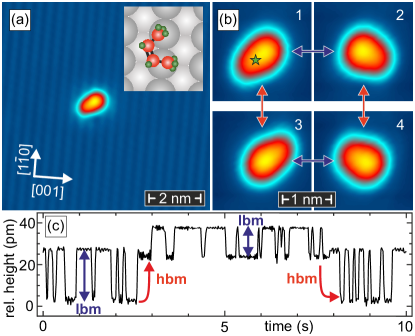
These reversible transitions result in four molecular adsorption geometries, labeled as states 1 to 4 in Fig. 1(b). When choosing a suitable tip position where the four states are distinguishable, such as the one marked by a green star in Fig. 1(b), we can determine the actual state of the molecule by recording the tip height. An example of the resulting telegraph noise is shown in Fig. 1(c). For s the apparent height fluctuates by about 25 pm, indicating lbm between states 1/2. Then, a more rare hbm to the high levels representing states 3/4 occurs, followed by lbm between these two states. Finally, at s another hbm sets the molecule back to states 1/2. Our observations are on full accordance with previous findings reported in Ref. Sainoo et al. (2005).
All data presented so far were measured with the STM tip positioned on top of the molecule. In order to investigate if the anisotropic structure of the Pd(110) surface also influences its charge transport properties in the ballistic regime we conducted measurements with the MONA technique Leisegang et al. (2018a). In short, MONA utilizes a charge carrier-driven molecular switching event, such as a tautomerization or rotation, to detect currents injected a few nanometers away. Since the activation barrier of the molecular rotation essentially represents a high pass filter of the detection process, only ballistic charge carrier, in this case with the threshold energy of the lbm, meV, can be detected. In this study we show that, by placing the STM tip and thereby the charge carrier injection point at different locations relative to the detector molecule, the influence of an anisotropic atomic lattice on ballistic transport can be evaluated. The measurement procedure is based on the cyclical repetition of three steps: First (i), the initial state of the molecule is probed by a topographic scan at non-invasive parameters ( mV, pA). Then (ii), the tip is moved to the excitation position at a distance from the detector molecule and charge carriers are injected at excitation parameters mV and nA. Eventually (iii), the final state of the c2b molecule is probed by another topographic scan at non-invasive parameters. Switching events between the rotational states are detected by comparing the STM images before and after each injection. The switching probability is obtained by calculating the average of numerous measurements. To avoid the excitation of two or more switching processes with a single pulse, the probability per pulse is kept well below %. The statistical standard variation of every data point presented in this work represents a minimum of 600 repetition cycles. Finally, we calculated the total electron yield by dividing the observed number of switching events through the amount of injected charge . The error bar for a calculated electron yield is given by .
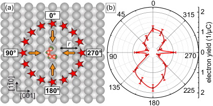
In a first set of direction-dependent measurements, the switching rate of a single c2b molecule was investigated by injecting charge carriers at a constant distance of nm from the molecule center under variation of the azimuthal angle. The 16 excitation positions are represented as red stars in Fig. 2(a) which for comparison also shows the surface atomic structure of Pd(110) (not in scale). As indicated by orange arrows, measurements performed at and probe the transport properties along the -oriented atomic rows of the Pd(110) surface, whereas data obtained at and give access to the transverse direction. The results are shown in polar coordinates in Fig. 2(b). On a qualitative level, we recognize a pronounced anisotropy with two main features: (I) Most apparent are broad maxima at and , where the electron yield is four to six times higher than in the minima around and . Furthermore, (II) the data exhibit more narrow maxima at and which are not as high as the values observed at and , but still exceed the surrounding minima by roughly a factor of three 111The atomic lattice presented in the background of Fig. 2(a) suggests an electron yield which is mirror-symmetric with respect to the and the direction of Pd(110). Whereas the data are mirror symmetric with respect to the direction, the broad lobe visible around is less extended than around . This asymmetry is caused by the fact that for the data presented in Fig. 2(b) exclusively switching events between states 1/2 connected by the lbm have been analyzed. As can be recognized in Fig. 1(b), the elongated tale of the of these states point towards the bottom edge of the STM image, thereby breaking mirror symmetry with respect to the axis..
To shed light on the question whether the striking anisotropy observed in Fig. 2 is driven by the dispersion relation or by scattering on single atomic rows, we performed MONA measurements at refined angle resolution. The data obtained around the direction are presented in Fig. 3. As sketched in Fig. 3(a) we took two sets of data at tip–molecule distances of nm (red stars) and nm (blue). In both cases 15 equidistant data points were taken, resulting in an angular resolution and , respectively. Comparison with the surface lattice, which is represented as true-to-scale spheres in Fig. 3(a), shows that the spacing of data points is well below the inter-row distance.
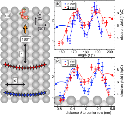
Figure 3(b) and (c) show the measured electron yield plotted versus the angle and the distance from the central dense-packed Pd row , respectively. Based on the results obtained at low angular resolution in Fig. 2(b), the findings presented here are quite surprising. Instead of a broad peak we now—at a much better resolution—recognize a narrow minimum located on the central row which is surrounded by a symmetric double peak structure. Comparing Fig. 3(b) and (c) reveals that the data coincide significantly better in the representation over the distance . Therefore, we conclude that the absolute charge carrier injection position on the row-wise structure rather than the relative direction of charge carrier propagation is relevant for the transport.
The observation of this narrow minimum suggests that the -oriented adatom rows posses a resistance which is enhanced as compared to the troughs in between. Moving the charge carrier injection point away from this row through the intermediate trough to the next adatom rows leads to an enhanced transport as detected by an increasing electron yield. Only if the tip is moved further sideways beyond this adjacent adatom row a steep decline in the measured electron yield is detected.
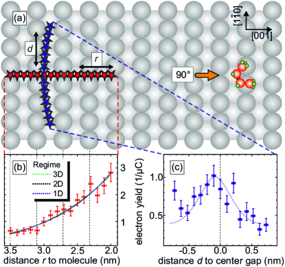
In a second set of measurements with sub-atomic resolution we investigated the charge carrier transport along the direction, i.e., transverse to the atomic rows. As marked by red stars in Fig. 4(a), we chose 16 equidistant excitation points at distances in the range between nm and nm from the molecular center. The respective electron yields are shown in Fig. 4(b). The distance dependence of the ballistic transport current can be described by , where the first term depicts the intensity decay in dimensions and the second term describes the exponential damping due to inelastic scattering on the characteristic length scale . Fitting the data to one- (1D), two- (2D), and three-dimensional (3D) transport results in very similar values of nm nm, represented by dashed lines in Fig. 4(b). This value is much lower than the inelastic mean free path usually found for very low electron energy, e.g., in noble metals Echenique et al. (2004), and might be caused by enhanced -band scattering in Pd Ladstädter et al. (2004) which also inhibits the unambiguous identification of the dimension of the transport channel.
A complementary series of measurements was taken at 15 points around along a circular arc with a radius of nm, see blue stars in Fig. 4(a), granting an angular resolution . The resulting electron yield is displayed in Fig. 4(c). We recognize a peak around the central atomic gap, nm, which quickly drops as the injection point is moved away from this position. Analysis reveals a peak width equivalent to the molecular adsorption site of about two atoms 222Again, the asymmetry around zero can be explained by the adsorption geometry of the molecule. Since the analysis is exclusively based on transitions between states 1/2, the elongation of the c2b along the axis breaks mirror symmetry with respect to the axis..
Discussion — The MONA data presented in Figs. 2 to 4 unambiguously show that ballistic charge carrier transport on Pd(110) surfaces is strongly anisotropic. Measurements performed at relatively low angular resolution reveal that electron transport is more efficient along the direction as compared to the direction. This anisotropy might, in principle, be caused either by potential wells formed by the adatoms rows or by an anisotropic band structure of the Pd(110) surface or by a combination of both effects. High angular resolution scans reveal two very narrow features along the high symmetry directions, i.e., a double peak in the direction and a single peak along . The data presented in Figs. 3 and 4 evidence that the width of both features correlate much better to the real space atomic lattice than the angle under which the charge injection is performed. These observations indicate that the adatoms, which create a row-wise structure on fcc(110) metal surfaces, serve as scattering potentials for the ballistic transport of hot charge carriers and that the band structure is of secondary relevance.
We speculate that the local density of states (LDOS) of the -derived bands responsible for the unusual short IMFP of Pd Ladstädter et al. (2004) accumulates at the adatom rows along the direction and decreases between them. This enhanced -LDOS would lead to a potential well-like periodic variation of the electrostatic potential with a high potential and strong scattering on top of the rows and potential troughs with much weaker scattering in between. Indeed, density functional theory calculations performed for Cu(110) also revealed a similar effect which results in a modulation by a few hundred meV Halldin Stenlid et al. (2019). As a result of this potential landscape, we measure a relatively low electron yield when the tip and the molecule are positioned on the same adatom row, since many electrons are scattered inelastically on their way from the injection point to the detector molecule. The assumption of scattering centers aligned along the adatom rows is also corroborated by the clear difference between the electron yield measure at nm for nm and nm, cf. Fig. 3(c). For nm we recognize a deeper minimum, indicating that the larger number of scatterers present along the longer path result in a stronger reduction of the transport. Moving the tip away from the center row to the adjacent trough reduces scattering and results in an increased transport towards the molecule and, thereby, to an increased electron yield. Only if the injection point is moved across the next adatom row its additional scattering potentials become effective, resulting in a strong decline of the transport.
Experiments along the direction further underpin the assumption of strongly localized scattering potentials. On the one hand we find that the inelastic mean free path (IMFP) of the charge carriers is on the order of one nanometer only, much shorter than what is usually observed for other noble metals. According to Ref. Ladstädter et al., 2004, the extraordinary reduction of the IMFP in Pd is caused by the strong contribution d-bands at the Fermi level. On the other hand the data presented in Fig. 4(c) reveal that scattering is reduced for charge carriers which propagate exactly perpendicular to dense-packed rows, as indicated by the higher electron yield. Therefore, we conclude that the row-wise atomic structure and the related surface potential is the main factor which determines the transport properties of the Pd(110) surface. However, we cannot exclude that the anisotropic band structure also has some, though much weaker effect.
In summary, our results show that the charge carrier-induced switching of a single cis-2-butene molecule can be utilized to detect the ballistic transport properties of Pd(110) on length scales of a few nanometers. We find a rich angular dependence with two sharp features, i.e., a dip along the -oriented atomic rows and a peak in the direction. These measurements provide evidence that the nanometer-scale charge transport properties of metallic surfaces is significantly influenced by scattering events on the atomic structure. We envision that similar measurements performed on materials more relevant for applications may not only lead to a better understanding of ballistic transport on atomic length scales but could also help optimizing the performance of nanoscale contacts and electrical junctions.
Acknowledgements.
We would like to thank S. Heinze and S. Haldar (Univ. Kiel) for insightful discussions. We acknowledge financial support by the Deutsche Forschungsgemeinschaft (DFG, German Research Foundation) through grant BO 1468/27-1 and under Germany’s Excellence Strategy through Würzburg–Dresden Cluster of Excellence on Complexity and Topology in Quantum Matter ct.qmat (EXC 2147, project-id 390858490).References
- Sverdlov et al. (2008) V. Sverdlov, E. Ungersboeck, H. Kosina, and S. Selberherr, “Current transport models for nanoscale semiconductor devices,” Mater. Sci. Eng.: Reports 58, 228–270 (2008).
- Tagliabue et al. (2020) G. Tagliabue, J. S. DuChene, A. Habib, R. Sundararaman, and H. A. Atwater, “Hot-hole versus hot-electron transport at Cu/GaN heterojunction interfaces,” ACS Nano 14, 5788–5797 (2020).
- Duhan et al. (2020) P. Duhan, V. R. Rao, and N. R. Mohapatra, “Effect of device dimensions, layout and pre-gate carbon implant on hot carrier induced degradation in HKMG nMOS transistors,” IEEE Trans. Dev. Mater. Reliab. 30, 555–561 (2020).
- Gabor et al. (2011) N. M. Gabor, J. C. W. Song, Q. Ma, N. L. Nair, T. Taychatanapat, K. Watanabe, T. Taniguchi, L. S. Levitov, and P. Jarillo-Herrero, “Hot carrier–assisted intrinsic photoresponse in graphene,” Science 334, 648–652 (2011).
- Bakulin et al. (2012) A. A. Bakulin, A. Rao, V. G. Pavelyev, P. H. M. van Loosdrecht, M. S. Pshenichnikov, D. Niedzialek, J. Cornil, D. Beljonne, and R. H. Friend, “The role of driving energy and delocalized states for charge separation in organic semiconductors,” Science 335, 1340–1344 (2012).
- Clavero (2014) C. Clavero, “Plasmon-induced hot-electron generation at nanoparticle/metal-oxide interfaces for photovoltaic and photocatalytic devices,” Nature Phot. 8, 95–103 (2014).
- Burger et al. (2019) A. M. Burger, R. Agarwal, A. Aprelev, E. Schruba, A. Gutierrez-Perez, V. M. Fridkin, and J. E. Spanier, “Direct observation of shift and ballistic photovoltaic currents,” Science Advances 5, eaau5588 (2019).
- Etheridge et al. (2019) H. G. Etheridge, K. R. Rusimova, and P. A. Sloan, “The nanometre limits of ballistic and diffusive hot-hole mediated nonlocal molecular manipulation,” Nanotechnology 31, 105401 (2019).
- Kanagawa et al. (2003) T. Kanagawa, R. Hobara, I. Matsuda, T. Tanikawa, A. Natori, and S. Hasegawa, “Anisotropy in conductance of a quasi-one-dimensional metallic surface state measured by a square micro-four-point probe method,” Phys. Rev. Lett. 91, 036805 (2003).
- Miccoli et al. (2015) I. Miccoli, F. Edler, H. Pfnür, and C. Tegenkamp, “The 100th anniversary of the four-point probe technique: the role of probe geometries in isotropic and anisotropic systems,” Jour. Phys.: Cond. Matter 27, 223201 (2015).
- Yang et al. (2016) J. Yang, D. Sordes, M. Kolmer, D. Martrou, and C. Joachim, “Imaging, single atom contact and single atom manipulations at low temperature using the new scientaomicron LT-UHV-4 STM,” Eur. Phys. J. Appl. Phys. 73, 10702 (2016).
- Voigtländer et al. (2018) B. Voigtländer, V. Cherepanov, S. Korte, A. Leis, D. Cuma, S. Just, and F. Lüpke, “Invited review article: Multi-tip scanning tunneling microscopy: Experimental techniques and data analysis,” Rev. Sci. Instr. 89, 101101 (2018).
- Kolmer et al. (2019) M. Kolmer, P. Brandimarte, J. Lis, R. Zuzak, S. Godlewski, H. Kawai, A. Garcia-Lekue, N. Lorente, T. Frederiksen, C. Joachim, D. Sanchez-Portal, and M. Szymonski, “Electronic transport in planar atomic-scale structures measured by two-probe scanning tunneling spectroscopy,” Nature Comm. 10, 1–10 (2019).
- Maksymovych et al. (2007) P. Maksymovych, D. B. Dougherty, X.-Y. Zhu, and J. T. Yates, “Nonlocal dissociative chemistry of adsorbed molecules induced by localized electron injection into metal surfaces,” Phys. Rev. Lett. 99, 016101 (2007).
- Sloan et al. (2010) P. A. Sloan, S. Sakulsermsuk, and R. E. Palmer, “Nonlocal desorption of chlorobenzene molecules from the surface by charge injection from the tip of a scanning tunneling microscope: Remote control of atomic manipulation,” Phys. Rev. Lett. 105, 048301 (2010).
- Ladenthin et al. (2015) J. Ladenthin, L. Grill, S. Gawinkowski, S. Liu, J. Waluk, and T. Kumagai, “Hot carrier-induced tautomerization within a single porphycene molecule on cu(111),” ACS Nano 9, 7287–7295 (2015).
- Schendel et al. (2016) V. Schendel, B. Borca, I. Pentegov, T. Michnowicz, U. Kraft, H. Klauk, P. Wahl, U. Schlickum, and K. Kern, “Remotely controlled isomer selective molecular switching,” Nano Letters 16, 93–97 (2016).
- Kügel et al. (2018) J. Kügel, M. Leisegang, and M. Bode, “Imprinting directionality into proton transfer reactions of an achiral molecule,” ACS nano 12, 8733–8738 (2018).
- Kügel et al. (2019) J. Kügel, T. Zenger, M. Leisegang, and M. Bode, “On the impact of geometrical factors on hot electron-induced tautomerization,” Journ. Phys. Chem. C 123, 17056–17061 (2019).
- Leisegang et al. (2018a) M. Leisegang, J. Kügel, L. Klein, and M. Bode, “Analyzing the wave nature of hot electrons with a molecular nanoprobe,” Nano Lett. 18, 2165–2171 (2018a).
- Leisegang et al. (2018b) M. Leisegang, M. Bode, and J. Kügel, “Analyzing the influence of substituents on proton tautomerization — comparison of tetra-tert-butyl phthalocyanine isomers,” Journ. Phys. Chem. C 122, 29633–29639 (2018b).
- Sainoo et al. (2003) Y. Sainoo, Y. Kim, T. Komeda, M. Kawai, and H. Shigekawa, “Observation of cis-2-butene molecule on Pd(110) by cryogenic STM: site determination using tunneling-current-induced rotation,” Surf. Sci. 536, L403–L407 (2003).
- Sainoo et al. (2005) Y. Sainoo, Y. Kim, T. Okawa, T. Komeda, H. Shigekawa, and M. Kawai, “Excitation of molecular vibrational modes with inelastic scanning tunneling microscopy processes: Examination through action spectra of cis-2-butene on Pd(110),” Phys. Rev. Lett. 95, 246102 (2005).
- Note (1) The atomic lattice presented in the background of Fig. 2(a) suggests an electron yield which is mirror-symmetric with respect to the and the direction of Pd(110). Whereas the data are mirror symmetric with respect to the direction, the broad lobe visible around is less extended than around . This asymmetry is caused by the fact that for the data presented in Fig.\tmspace+.1667em2(b) exclusively switching events between states 1/2 connected by the lbm have been analyzed. As can be recognized in Fig.\tmspace+.1667em1(b), the elongated tale of the of these states point towards the bottom edge of the STM image, thereby breaking mirror symmetry with respect to the axis.
- Echenique et al. (2004) P. M. Echenique, R. Berndt, E. V. Chulkov, Th. Fauster, A. Goldmann, and U. Höfer, “Decay of electronic excitations at metal surfaces,” Surf. Sci. Rep. 52, 219–317 (2004).
- Ladstädter et al. (2004) F. Ladstädter, U. Hohenester, P. Puschnig, and C. Ambrosch-Draxl, “First-principles calculation of hot-electron scattering in metals,” Phys. Rev. B 70, 235125 (2004).
- Note (2) Again, the asymmetry around zero can be explained by the adsorption geometry of the molecule. Since the analysis is exclusively based on transitions between states 1/2, the elongation of the c2b along the axis breaks mirror symmetry with respect to the axis.
- Halldin Stenlid et al. (2019) J. Halldin Stenlid, A. J. Johansson, and T. Brinck, “The local electron attachment energy and the electrostatic potential as descriptors of surface–adsorbate interactions,” Phys. Chem. Chem. Phys. 21, 17001–17009 (2019).