Effect of Impurities on Charge and Heat Transport in Tubular Nanowires
Abstract
We calculate the charge and heat currents carried by electrons, originating from a temperature gradient and a chemical potential difference between the two ends of tubular nanowires with different geometries of the cross-sectional areas: circular, square, triangular, and hexagonal. We consider nanowires based on InAs semiconductor material, and use the Landauer-Büttiker approach to calculate the transport quantities. We include impurities in the form of delta scatterers and compare their effect for different geometries. The results depend on the quantum localization of the electrons along the edges of the tubular prismatic shell. For example, the effect of impurities on the charge and heat transport is weaker in the triangular shell than in the hexagonal shell, and the thermoelectric current in the triangular case is several times larger than in the hexagonal case, for the same temperature gradient.
I Introduction
Down to the nanoscale, the closeness of constituting atoms to material boundaries and high surface area to volume ratio provides interesting quantum physical phenomena. Nanostructures exhibit unique properties that are different from those of their bulk counterparts. Among these nanostructures, nanowires have attracted considerable attention due to their potential applications in modern technologies. Nanowires of small size are ideal for miniaturized devices such as transistors Duan et al. (2003), batteries Park et al. (2007), and sensors Fakhri et al. (2022a, b). Also, their high surface area to volume ratio increases the efficiency of energy storage, and provides unique physical and chemical properties such as improved electrical conductivity, increased strength, and enhanced catalytic activity Zhou et al. (2019); Yu et al. (2018); Wang et al. (2013). The properties of nanowires depend on their material, as they can be made from metals, semiconductors, and insulators, but also on their internal geometry.
Semiconductor nanowires are potential candidates for several fields of technology such as nanoelectronics Xu et al. (2010); Lu and Lieber (2007); Bansal et al. (2020); Alexsandro dos Santos et al. (2021); Yuan et al. (2021), quantum information processing Hu et al. (2007), solar cells Kempa et al. (2008); Gao et al. (2022), biological sensors Cui et al. (2001), thermoelectrics and energy conversion devices Boukai et al. (2008); Hochbaum et al. (2008); Li et al. (2021), and integrated circuits Nam et al. (2009). In many of these applications understanding the charge and heat current is crucial. Thermoelectric devices demand a high charge current associated with low heat transport to reach high efficiency Snyder and Toberer (2008); Peri et al. (2022); Heris et al. (2020), while nanoelectronic devices necessitate high heat transport and sinks to take heat out from nano chips Schelling et al. (2005). In particular, core-shell nanowires, which are radial heterojunctions of two or more different semiconductor materials, enable the control of charge and heat transfer through specific geometry. In such structures, electronic properties can be determined by the band alignment between materials, core size, and shell thickness. Similarly, heat transport can be guided or trapped through core-shell nanowires Heris et al. (2022a).
Core-shell nanowires with a doped shell and an undoped core are tubular conductors, such that conduction takes place only in the shell Gül et al. (2014). It is also possible to achieve tubular nanowires by etching the core part Haas et al. (2013). Tubular nanowires, with length much greater than their diameter, have special mechanical, electrical, and optical properties, than ordinary full body nanowires. Tubular nanowires can maintain their shape and structure even under extreme conditions, such as high temperatures or pressures Noël (2014); Li et al. (2022). Also, high electrical conductivity due to the elimination of phonon scattering, and high chemical stability are other advantages of tubular nanowires Liu et al. (2010); Skákalová et al. (2006); Adler-Abramovich et al. (2006); Chunfeng et al. (2007).
Semiconductor core-shell nanowires based on III-V materials are most commonly prismatic. The typical shape of the cross-section is hexagonal Blömers et al. (2012); Petronijevic et al. (2017); Chen et al. (2002), but other prismatic shapes can also be fabricated, like square Fan et al. (2006) or triangular Heurlin et al. (2015); Khosravi et al. (2020). The prismatic geometry of core-shell nanowires, especially tubular nanowires, presents a unique window to important features. These include conductance and electron localization Torres et al. (2018); Sitek et al. (2015), quantum confinement effect over charge carriers Tian et al. (2012), interacting several Majorana states with each other Manolescu et al. (2017); Klausen et al. (2020) and inducing the sign reversal of the electric current generated by the temperature gradient in presence of a transversal magnetic field Erlingsson et al. (2017). Amongst different materials for prismatic nanowires, InAs is one the most studied. Different approaches for controlling grow Mandl et al. (2006); Tomioka et al. (2008) and lattice Dick et al. (2010) features, ultrahigh electron mobility Ford et al. (2009), and direct-narrow band gap Liu et al. (2013), are some of the advantages of this material.
In tubular nanowires apart of the geometry mainly three factors lead to changes in charge and heat current: surface roughness, impurities and phonons. Surface roughness leads to a reduction in charge current but practically it is easy to estimate the range of this deviation for different materials Ziman (2001). It had been shown that electron-phonon interaction can be neglected in thin shells Choi et al. (2003). Also, experimentally it is possible to heat up just electrons, while the phonons are kept frozen Van Houten et al. (1992); Molenkamp et al. (1990). Consequently, the electron-phonon coupling can be assumed to be negligible. Impurities play a significant role in the conduction feature of tubular nanowires, and it is different for transported charge and heat current for each cross-section with respect to chemical potential bias or temperature gradient. Different numbers of impurities or varying intensities show distinct behavior in each case of cross-section geometry. Understanding the combination of heat and charge current is essential in many cases of nanoscale studies, and the purpose of this work is to provide a comprehensive view of impurities’ effect on electronic conduction of tubular nanowires. We study the effect of the density of the impurities, and of the strength of the associated potential, on the charge and heat currents, in prismatic shells. Due to the fact that nowadays it is feasible to fabricate tubular nanowires with the desired cross-section and different doping variations, our study can be useful to establish a direct relation between different cross-sections and transport properties of core-shell nanowires.
The paper is structured in the following sections: Section 2 contains our model and methodology. In Section 3 we present the results, in particular we show how the presence of impurities affects conductance through wires of different cross sections. Further, we focus on wires having hexagonal and triangular cross sections and we study the impact of the number and strength of impurities on the conductance. Finally, Section 4 contains the conclusions.
II Model and methods
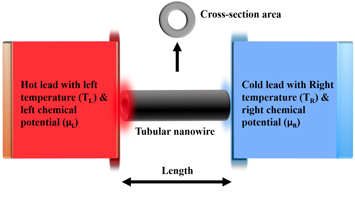
Our model is a core-shell nanowire with a finite length and with different cross-sectional geometries. The different shapes of the interface between the core and the shell lead to different energies for each electronic state. Consequently, the physical properties of the nanowire will depend on the geometry of its cross section. In the present work we consider the core material not doped, i. e. it behaves like an insulator. The only role of the core is to define the geometry of the shell. We assume the conduction of electrons occurring solely through the shell, which is assumed n-doped. We consider a temperature gradient and different chemical potentials between the two ends or the nanowire, by assuming it placed between two macroscopic leads, as illustrated in Figure 1.
The disorder is represented by localized repulsive potential barriers, mimicking the effect of impurities present in the nanowire. All impurities are assumed of identical strength, and also fixed and rigid. They are randomly distributed within the volume of the shell, using a random number generator. The idea behind this kind of impurity model is that all physical effects on the electronic conduction occur due to the sequential scattering of an electron on individual impurities, when the distance between the electron and impurity is very short, and then the electron propagates freely until eventually meeting the next impurity, where another scattering event occurs. Then for each example, we consider a particular number of impurities whose strength varies within a certain range.
We calculate the electronic charge and heat currents for four cross section shapes: cylindrical, hexagonal, square and triangular, as shown in Figure 2. In all cases the external radius of the nanowire is 50 nm (i.e. the radius of the circle encompassing the entire cross section) and the shell thickness is nm, so that conduction takes place in the narrow shell cross-sectional area. All nanowires have a length of 500 nm. The number of occupied quantum states in the nanowire, which is also the number of electrons participating to the transport, is up to about 10000. In terms of carrier density, it corresponds to a doping level of the order of , but in experimental nanowires the carrier concentration is also controlled with electrostatic gates.


The Hamiltonian of the nanowire consists of a longitudinal and a transverse term. The transverse Hamiltonian is discretized in polar coordinates Daday et al. (2011); Sitek et al. (2016). A specific cross-section of the polygonal shell, defined on a set of lattice of points, is obtained from a circular disk, after excluding every point from the lattice which stands outside the shell boundaries Torres et al. (2018). The electron effective mass is , as for bulk InAs. We calculate heat current and electrical current driven by the temperature gradient and chemical potential bias applied between two ends of nanowire using the Landauer-Buttiker approach:
| (1) |
| (2) |
where is the transmission function, and
is the Fermi function for the left (L) or right (R) reservoir with chemical potential and temperature (and denoting Boltzmann’s constant).
For clarity reasons we study the conduction under the temperature gradient case and chemical potential bias case separately. So in each case one type of bias is constant and the other one is variable. The chemical potential bias is always present at the two ends of the nanowire, and in each step of the calculation we change the left and the right reservoir values simultaneously, but keeping meV fixed. In all cases, we consider the first 10 transverse modes in our numerical calculation regardless of geometries or impurities variation.
Different cross-sectional areas lead to different energy spectra for each shape and consequently different chemical potential windows appear. Due to this reason, first we need to find the maximum and minimum possible values of the chemical potentials, corresponding to each specific cross-section. Then, the entire energy interval between the lowest and highest energy states (corresponding to the first 10 transverse modes) is explored step-wise. During this series of calculations, i. e. in the presence of a chemical potential bias, we consider no temperature gradient, and K. To compute the currents, the energy limits are considered between the ground state and the highest available state for each cross-section. For instance, this range for circular cross section is 35-85 meV, and for triangle cross section is 120-220 meV.
In the case of a temperature gradient, we fix K. In the first step, we set K and K and then we increase the temperature of both sides simultaneously. This process is repeated several times, while the left temperature varies between 36 - 420 K. The temperature gradient effect on the conductance is calculated using the same chemical potentials at the left and right end of the nanowire. For each geometry these values are calculated as , where the miniminum and maximum values are equal to the minimum and maximum energy in the computed electronic spectra, respectively. For example, in the case of the circular cross section meV and meV, and we set both chemical potentials at meV. By applying the same rule to the other geometries, chemical potential values are meV, meV, and meV, for the hexagon, square and triangle, respectively.
III Results and discussion
III.1 Impurities in different cross section geometries
Tubular nanowires increase thermoelectric current due to the lateral electron confinement Balaghi et al. (2021); Ramayya et al. (2007) and decrease heat transport due to the strong suppression of phonons with a diameter below the phonon mean free path Heris et al. (2022a); Juntunen et al. (2019). Core-shell nanowires with polygonal cross-sections show a stronger electron localization at the corners than on the sides of the polygon. The energy structure of shells with polygonal cross-sections has a strong dependence on the number of corners Estarellas and Serra (2015); Sitek et al. (2015). There is a remarkable energy gap between the states localized at corners and the next states which stand on polygon’s sides. This gap increases with decreasing the shell thickness or the number of corners Heris et al. (2022b). The lowest energy states are always localized in the corners. The polygonal shell properties differ considerably from each other because of the complexity of the localization of low energy states.
Implementing disorder in the shell such as impurities makes these properties even more complex, but at the same time with some promising results. Figure 3 presents charge and heat current versus the left chemical potential and temperature for tubular nanowires with different cross-sections in the presence of impurities. All implemented impurities are repulsive with the strength of 10 meV. Despite different energy states for each cross-section, the charge current for all geometries follows the transmission function and the energy window associated with the chemical potential. So increasing the chemical potential allows a larger number of states to participate in the transmission, which leads to a higher charge current. This occurs for pure wires, and for those with impurities as well.
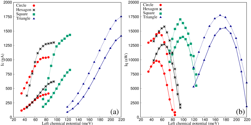
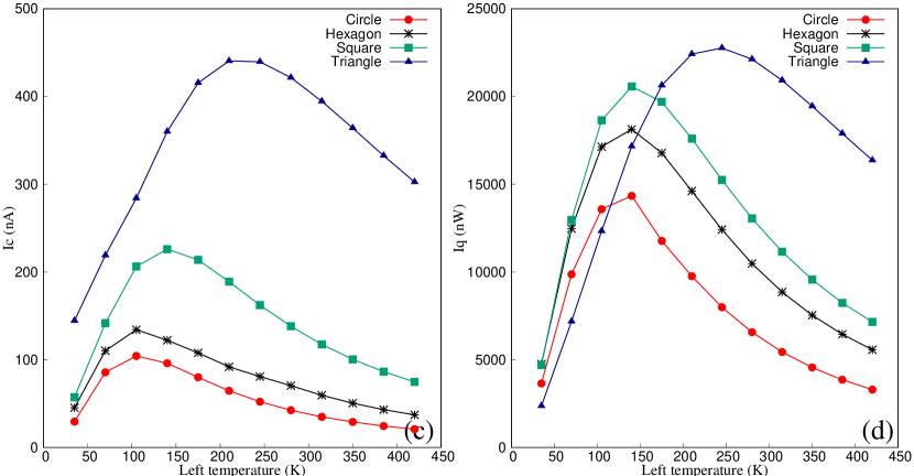
It is clear from all curves in Figure 3 that the presence of impurities leads to a reduction in charge and heat current values with respect to temperature or chemical potential. These reductions can be seen easily as difference between the magnitude of currents with no impurities (dashed lines curves) and the magnitude with impurities (solid lines curves) with the same color. In Figure 3(a) we can see that despite having the same area and number of impurities (10000 impurities with a magnitude of 10 meV) for all polygonal shapes, the triangular shell can carry charge way better than others. The cross-sections with fewer corners have higher values of thermoelectric current. This can be explained by the fewer transverse modes, but with steeper energy dispersion at the energy reached by higher values of of the variable chemical potential. While in the case of heat current, the variation with the nanowire shape is smaller.
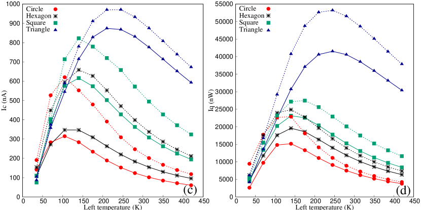
The maximum heat current occurs in the absence of impurities and above 100 K. The location of this maximum varies with respect to the geometry of the nanowire, and it decreases by increasing the number of impurities. Using the cross sectional area of the nanowire it is possible to calculate the thermal conductivity . For instance, by considering the heat current W at 250 K and , our thermal conductivity is approximately 26 W/mK. Some experimental studies present comparable results for the thermal conductivity of InAs nanowires Zhou et al. (2011); Ren et al. (2014).
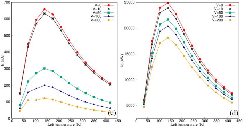
We can see an order between different cross sections in charge and heat transported by electrons as a function of both left chemical potential and left temperature. Also, the reduction of currents due to impurities is different for each geometry. By using the same number of impurities in different cross-sections, we can see that in the case of the circular cross-section the charge and heat transport decrease dramatically in comparison to other geometries. On the average the circular cross-section shows 65% reduction of the charge current values and 30% reduction of the heat current values in the presence of impurities. The corresponding values for the triangular cross-section are 10% and 15% , respectively (see Figure 3(a) and (b)). Figure 3(c) and (d) also present the values of charge and heat current for pure shells and their reduction in the presence of impurities with respect to the left side temperature. These reductions are smaller than in the case of a chemical potential bias. Despite the presence of the impurities, with the magnitude of 10 meV, the triangular shell still shows the highest values of both electrical and thermal currents.
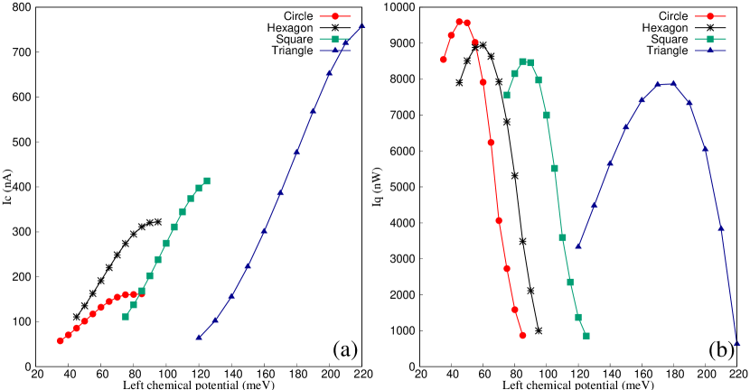
Considering impurities in a system as a disorder, one should take into account both the number and strength of implemented impurities. Therefore, in the next series of calculations instead of the high number of impurities we consider a small amount of them, but with stronger potentials, to see the variation of thermoelectric properties again as a function of chemical potential and temperature for different shell cross sections. In all cases, we implement 300 impurities with a strength of 200 meV. According to Figure 4(a) we can see a again significant reduction in the magnitude of both electrical and heat current for all geometries. But interestingly, implementing impurities with strong potentials leads to a reduction of near 70% for the circular cross-section and 48% in the case of the triangular cross-section. The reduction of the heat transport for the circular cross section is much weaker than for triangular one, which results in the reversed order of the curves. Compare Figure 3(a) and Figure 4(a) for values, and compare Figure 3(b) and Figure 4(b) for values. This noticeable shift in and magnitudes and sequence order is not limited to chemical potential bias and we can see the same behavior also in the case of the temperature gradient.
III.2 Effect of the number of impurities
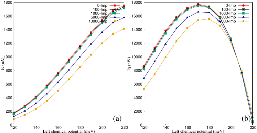
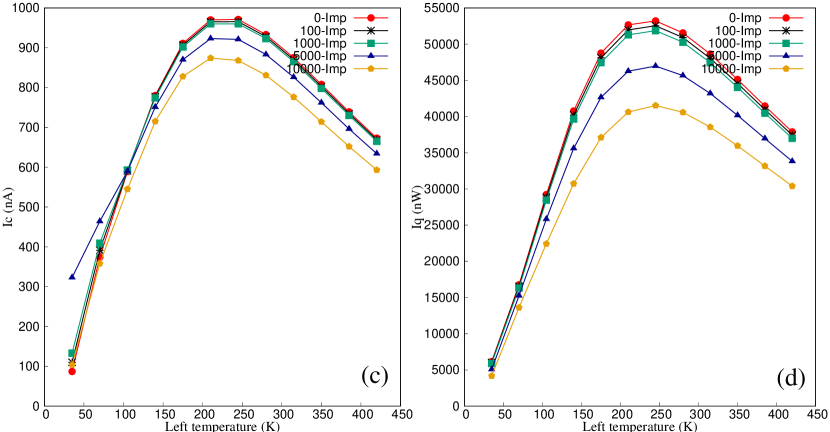
Figures 3 and 4 present the effect of a high number of impurities and of impurities with strong associated potentials on the electronic properties of nanowires with different cross sections. Results point out that nanowires with triangular cross-sections show the highest electrical current with respect to both temperature gradient and chemical potential bias. Also, the heat current has the largest variation for triangular nanowires, compared to the other geometries, in presence of impurities. Due to these reasons, and based on the fact that the typical shape of the cross section for III-V materials is hexagonal, we choose the triangular and hexagonal shells to explore further the effects of impurities in these cases. We consider in our systems impurities with different numbers for each case (0, 100, 1000, 5000, 10000) with a fixed magnitude of 10 meV. Increasing the number of impurities always leads to a reduction in values of both electrical current and heat current regardless of chemical potential or temperature gradient variation.
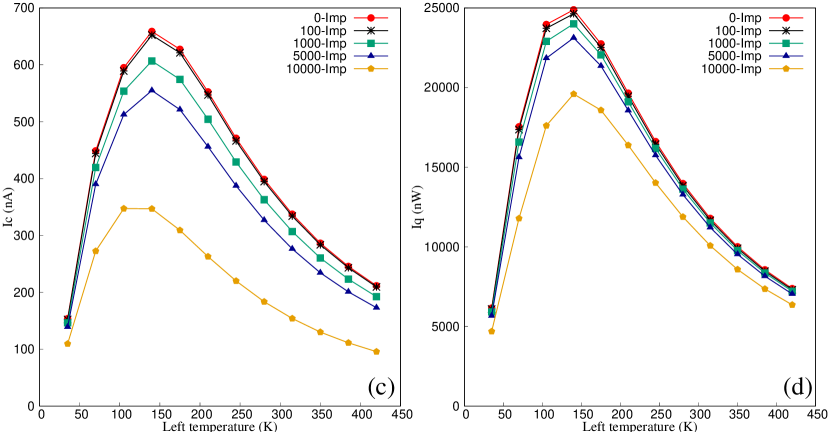
A small number of impurities will not play a noticeable role in the reduction of conduction. As can be seen in Figure 5 (a) and (c) the presence of up to 1000 impurities does not affect much the charge current, but further increase of the number of impurities results in the reduction of 15-25% in the current for the triangular shell. The current reduction due to impurities is much larger for hexagonal shells, where the percentage drop may be twice larger than in the case of triangular wire, Figure 6. The process that causes the current reduction here is scattering, each impurity acts as a scattering center, and thus the effect increases with the number of impurities in the wire. However, the stronger localization of electrons at corners in the triangular geometry, where the corners are sharper than in the hexagonal case, leads to a more robust electronic states in the triangular case, and thus to currents less sensitive to impurities.
III.3 Effect of the strength of impurities
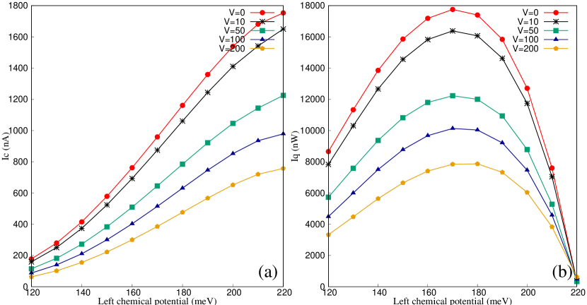
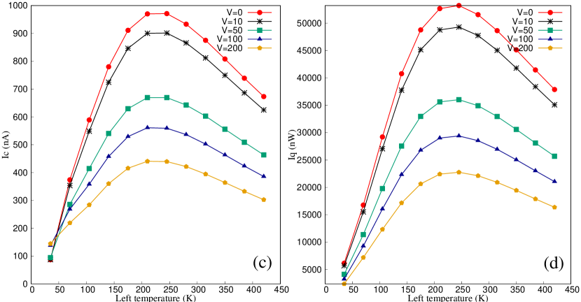
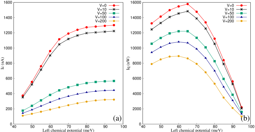
In this section we consider a small number of impurities (300) with the magnitudes of their associated potential varying from zero (pure, or clean shell) to 200 meV. Such systems, i.e. with a low number of high strength impurities, are particularly interesting because they can model different physical situations. For instance, these impurities can be considered as small, but heavy ionized doping concentrations Sadi et al. (2019). And in some cases, the scattering of free carriers by phonons can be modelled with such strong potentials Markussen et al. (2007); Fonoberov and Balandin (2006).
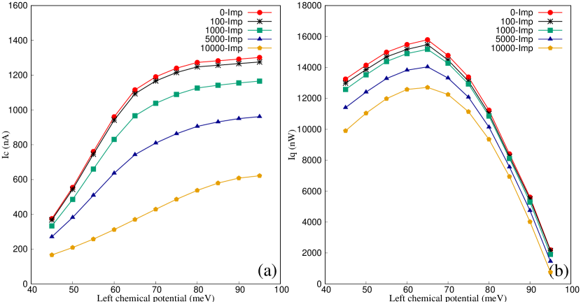
Contrary to the case of large number of low strength impurities, in the case of the small number of impurities with high strength there is a large deviation from the clean shell for all studied cases (Figure 7 and Figure 8). The reduction of the currents becomes 50% for triangle shell and 85% in some cases for hexagonal shells. In Figure 7(a) we show the variation of the currents with the increasing the left chemical potential. By shifting the left chemical potential values we increase the transmission window, and thus allow, more states to participate to the transport, which leads to a higher electrical current. This increase in values of the electrical current of triangle shells with no impurities reaches almost ninefold of the initial value, while in shells with impurities this increase is strongly suppressed.
In Figure 7 (b) we show the heat current as a function of the left chemical potential for a few values of impurity strength. The current decrease is significant and reaches 12-40% in the peaks for stronger impurities. Both electrical and heat currents, as functions of left temperature, also decrease in presence of stronger impurities, Figure 7 (c) and (d). A close look at the values of and in Figure 7 (c) and (d), with respect to the shell with no impurity indicates interesting features. Both the charge and the heat currents show peaks between 200-250 K. And in this temperature range, with strong impurities in the system, we obtain 50% reduction of , while for the same temperature range the reduction of reaches 65-70%. So in the presence of a temperature gradient, in the triangular shells, with strong impurities, we can reach a system that suppresses electrical current less than heat current. This feature is very desirable in thermoelectric applications.
In hexagonal shells, the charge current in the presence of intense impurities shows a significant reduction, of on the average, when the chemical potential and temperature are varied. In all cases the charge current in the hexagonal shell is much stronger suppressed than in the triangular shell. While heat current in hexagonal shells shows a smaller reduction in comparison to triangle shells. By comparing Figure 7 and Figure 8 one can see that strong impurities lead to different behavior of the charge and heat current of hexagonal and triangular shells. For the triangular shell, the heat current is more suppressed in presence of intense impurities than the charge current, while the opposite occurs in the case of a hexagonal shell. By considering values of charge and heat current in hexagonal shells (Figure 8) in the presence of intense impurities, this shell is a good candidate for removing and expunging heat.
IV Conclusions
We studied the effect of the number and strength of impurities on the charge and heat currents driven by a temperature or chemical potential bias, for different cross-sectional geometries of tubular nanowires. We began with a clean shell (or pure, i. e. without impurities) in each case and increased gradually the number of impurities. As expected these impurities lead to an increase of the scattering of electrons, and due to this reason the charge and heat current transported by carriers always decrease. We could obtain a further reduction of the currents by using a smaller number of impurities, but with a stronger associated potential. This effect may be also expected, since in general the impurity effects scale linearly with the impurity density, but quadratically with their strength. However, we show that the charge and heat current, and the effect of impurities on them, depend on the shell geometry. In the presence of impurities the triangular shell carries a charge current almost four times more than the hexagonal shell, for the same temperature gradient (35 K). While the heat current for the triangular shell is only 15% higher than hexagonal shells. An interesting result is that the effect of impurities on the charge and heat transport is smaller in the triangular shell than in the hexagonal shell. The reason is that the localization of the electrons on the corner and on the sides of the polygonal shell is more pronounced in the triangular case, which leads to higher energy intervals between different transverse states and consequently to a reduced scattering, compared to the hexagonal case.
In conclusion, the interplay of the geometry and impurities leads to complex effects that may favor an increase of the thermoelectric efficiency of semiconductor based tubular or core-shell nanowires, that needs to be experimentally investigated.
Acknowledgment
This work was supported by the Icelandic Research Fund, Grant 195943-051 and 229078-051.
References
- Duan et al. (2003) X. Duan, C. Niu, V. Sahi, J. Chen, J. W. Parce, S. Empedocles, and J. L. Goldman, Nature 425, 274 (2003).
- Park et al. (2007) M.-S. Park, G.-X. Wang, Y.-M. Kang, D. Wexler, S.-X. Dou, and H.-K. Liu, Angewandte Chemie International Edition 46, 750 (2007).
- Fakhri et al. (2022a) E. Fakhri, M. Sultan, A. Manolescu, S. Ingvarsson, and H. Svavarsson, in 2022 International Semiconductor Conference (CAS) (IEEE, 2022) pp. 163–166.
- Fakhri et al. (2022b) E. Fakhri, R. Plugaru, M. T. Sultan, T. Hanning Kristinsson, H. Örn Árnason, N. Plugaru, A. Manolescu, S. Ingvarsson, and H. G. Svavarsson, Sensors 22, 6340 (2022b).
- Zhou et al. (2019) G. Zhou, L. Xu, G. Hu, L. Mai, and Y. Cui, Chemical reviews 119, 11042 (2019).
- Yu et al. (2018) K. Yu, X. Pan, G. Zhang, X. Liao, X. Zhou, M. Yan, L. Xu, and L. Mai, Advanced Energy Materials 8, 1802369 (2018).
- Wang et al. (2013) Y. Wang, T. Wang, P. Da, M. Xu, H. Wu, and G. Zheng, Advanced materials 25, 5177 (2013).
- Xu et al. (2010) S. Xu, Y. Qin, C. Xu, Y. Wei, R. Yang, and Z. L. Wang, Nature nanotechnology 5, 366 (2010).
- Lu and Lieber (2007) W. Lu and C. M. Lieber, Nature materials 6, 841 (2007).
- Bansal et al. (2020) S. Bansal, K. Prakash, K. Sharma, N. Sardana, S. Kumar, N. Gupta, and A. K. Singh, Nanotechnology 31, 405205 (2020).
- Alexsandro dos Santos et al. (2021) E. Alexsandro dos Santos, M. V. P. dos Santos, R. B. Campanelli, P. G. Pagliuso, J. Bettini, K. R. Pirota, and F. Béron, Nanoscale Advances 3, 3251 (2021).
- Yuan et al. (2021) W. Yuan, G. Tutuncuoglu, A. T. Mohabir, R. Thorpe, L. C. Feldman, M. A. Filler, and J. W. Shan, ACS Applied Nano Materials 4, 3852 (2021).
- Hu et al. (2007) Y. Hu, H. O. Churchill, D. J. Reilly, J. Xiang, C. M. Lieber, and C. M. Marcus, Nature nanotechnology 2, 622 (2007).
- Kempa et al. (2008) T. J. Kempa, B. Tian, D. R. Kim, J. Hu, X. Zheng, and C. M. Lieber, Nano letters 8, 3456 (2008).
- Gao et al. (2022) S. Gao, X. Zhao, Q. Fu, T. Zhang, J. Zhu, F. Hou, J. Ni, C. Zhu, T. Li, Y. Wang, et al., Journal of Materials Science & Technology 126, 152 (2022).
- Cui et al. (2001) Y. Cui, Q. Wei, H. Park, and C. M. Lieber, science 293, 1289 (2001).
- Boukai et al. (2008) A. I. Boukai, Y. Bunimovich, J. Tahir-Kheli, J.-K. Yu, W. A. Goddard Iii, and J. R. Heath, nature 451, 168 (2008).
- Hochbaum et al. (2008) A. I. Hochbaum, R. Chen, R. D. Delgado, W. Liang, E. C. Garnett, M. Najarian, A. Majumdar, and P. Yang, Nature 451, 163 (2008).
- Li et al. (2021) Y. Li, G. Wang, M. Akbari-Saatlu, M. Procek, and H. H. Radamson, Frontiers in Materials 8, 611078 (2021).
- Nam et al. (2009) S. Nam, X. Jiang, Q. Xiong, D. Ham, and C. M. Lieber, Proceedings of the National Academy of Sciences 106, 21035 (2009).
- Snyder and Toberer (2008) G. J. Snyder and E. S. Toberer, Nature materials 7, 105 (2008).
- Peri et al. (2022) L. Peri, D. Prete, V. Demontis, V. Zannier, F. Rossi, L. Sorba, F. Beltram, and F. Rossella, Nano Energy 103, 107700 (2022).
- Heris et al. (2020) H. R. Heris, M. Kateb, S. I. Erlingsson, and A. Manolescu, Nanotechnology 31, 424006 (2020).
- Schelling et al. (2005) P. K. Schelling, L. Shi, and K. E. Goodson, Materials Today 8, 30 (2005).
- Heris et al. (2022a) H. R. Heris, M. Kateb, S. I. Erlingsson, and A. Manolescu, Surfaces and Interfaces 30, 101834 (2022a).
- Gül et al. (2014) Ö. Gül, N. Demarina, C. Blömers, T. Rieger, H. Lüth, M. Lepsa, D. Grützmacher, and T. Schäpers, Physical Review B 89, 045417 (2014).
- Haas et al. (2013) F. Haas, K. Sladek, A. Winden, M. Von der Ahe, T. Weirich, T. Rieger, H. Lüth, D. Grützmacher, T. Schäpers, and H. Hardtdegen, Nanotechnology 24, 085603 (2013).
- Noël (2014) M. Noël, Physical properties and structural stability of carbon nanotubes under extreme conditions, Ph.D. thesis, Luleå tekniska universitet (2014).
- Li et al. (2022) B. Li, S. Li, K. Shi, X. Zhang, S. Yang, D. Pan, L. Liu, Y. Nan, X. Zhu, X. Song, et al., Acta Materialia 228, 117776 (2022).
- Liu et al. (2010) F. Liu, C. Shen, Z. Su, X. Ding, S. Deng, J. Chen, N. Xu, and H. Gao, Journal of Materials Chemistry 20, 2197 (2010).
- Skákalová et al. (2006) V. Skákalová, A. B. Kaiser, Y.-S. Woo, and S. Roth, Physical Review B 74, 085403 (2006).
- Adler-Abramovich et al. (2006) L. Adler-Abramovich, M. Reches, V. L. Sedman, S. Allen, S. J. Tendler, and E. Gazit, Langmuir 22, 1313 (2006).
- Chunfeng et al. (2007) D. Chunfeng, Z. Xuexi, and W. Dezun, Materials Letters 61, 904 (2007).
- Blömers et al. (2012) C. Blömers, T. Rieger, P. Zellekens, F. Haas, M. Lepsa, H. Hardtdegen, Ö. Gül, N. Demarina, D. Grützmacher, H. Lüth, et al., Nanotechnology 24, 035203 (2012).
- Petronijevic et al. (2017) E. Petronijevic, M. Centini, A. Belardini, G. Leahu, T. Hakkarainen, and C. Sibilia, Optics Express 25, 14148 (2017).
- Chen et al. (2002) Y. Chen, D. A. Ohlberg, and R. S. Williams, Journal of Applied Physics 91, 3213 (2002).
- Fan et al. (2006) H. Fan, M. Knez, R. Scholz, K. Nielsch, E. Pippel, D. Hesse, U. Gösele, and M. Zacharias, Nanotechnology 17, 5157 (2006).
- Heurlin et al. (2015) M. Heurlin, T. Stankevic, S. Mickevicius, S. Yngman, D. Lindgren, A. Mikkelsen, R. Feidenhans’l, M. T. Borgstrom, and L. Samuelson, Nano Letters 15, 2462 (2015).
- Khosravi et al. (2020) F. Khosravi, S. A. Hosseini, and B. A. Hamidi, Thin-Walled Structures 148, 106591 (2020).
- Torres et al. (2018) M. U. Torres, A. Sitek, S. I. Erlingsson, G. Thorgilsson, V. Gudmundsson, and A. Manolescu, Physical Review B 98, 085419 (2018).
- Sitek et al. (2015) A. Sitek, L. Serra, V. Gudmundsson, and A. Manolescu, Physical Review B 91, 235429 (2015).
- Tian et al. (2012) Y. Tian, M. R. Sakr, J. M. Kinder, D. Liang, M. J. MacDonald, R. L. Qiu, H.-J. Gao, and X. P. Gao, Nano letters 12, 6492 (2012).
- Manolescu et al. (2017) A. Manolescu, A. Sitek, J. Osca, L. Serra, V. Gudmundsson, and T. D. Stanescu, Physical Review B 96, 125435 (2017).
- Klausen et al. (2020) K. O. Klausen, A. Sitek, S. I. Erlingsson, and A. Manolescu, Nanotechnology 31, 354001 (2020).
- Erlingsson et al. (2017) S. I. Erlingsson, A. Manolescu, G. A. Nemnes, J. H. Bardarson, and D. Sanchez, Physical review letters 119, 036804 (2017).
- Mandl et al. (2006) B. Mandl, J. Stangl, T. Mårtensson, A. Mikkelsen, J. Eriksson, L. S. Karlsson, G. Bauer, L. Samuelson, and W. Seifert, Nano letters 6, 1817 (2006).
- Tomioka et al. (2008) K. Tomioka, J. Motohisa, S. Hara, and T. Fukui, Nano letters 8, 3475 (2008).
- Dick et al. (2010) K. A. Dick, C. Thelander, L. Samuelson, and P. Caroff, Nano letters 10, 3494 (2010).
- Ford et al. (2009) A. C. Ford, J. C. Ho, Y.-L. Chueh, Y.-C. Tseng, Z. Fan, J. Guo, J. Bokor, and A. Javey, Nano Letters 9, 360 (2009).
- Liu et al. (2013) Z. Liu, T. Luo, B. Liang, G. Chen, G. Yu, X. Xie, D. Chen, and G. Shen, Nano Research 6, 775 (2013).
- Ziman (2001) J. M. Ziman, Electrons and phonons: the theory of transport phenomena in solids (Oxford university press, 2001).
- Choi et al. (2003) Y.-M. Choi, D.-S. Lee, R. Czerw, P.-W. Chiu, N. Grobert, M. Terrones, M. Reyes-Reyes, H. Terrones, J.-C. Charlier, P. Ajayan, et al., Nano Letters 3, 839 (2003).
- Van Houten et al. (1992) H. Van Houten, L. Molenkamp, C. Beenakker, and C. Foxon, Semiconductor Science and Technology 7, B215 (1992).
- Molenkamp et al. (1990) L. Molenkamp, H. Van Houten, C. Beenakker, R. Eppenga, and C. Foxon, Physical Review Letters 65, 1052 (1990).
- Daday et al. (2011) C. Daday, A. Manolescu, D. Marinescu, and V. Gudmundsson, Physical Review B 84, 115311 (2011).
- Sitek et al. (2016) A. Sitek, G. Thorgilsson, V. Gudmundsson, and A. Manolescu, Nanotechnology 27, 225202 (2016).
- Balaghi et al. (2021) L. Balaghi, S. Shan, I. Fotev, F. Moebus, R. Rana, T. Venanzi, R. Hübner, T. Mikolajick, H. Schneider, M. Helm, et al., Nature communications 12, 1 (2021).
- Ramayya et al. (2007) E. B. Ramayya, D. Vasileska, S. M. Goodnick, and I. Knezevic, IEEE transactions on nanotechnology 6, 113 (2007).
- Juntunen et al. (2019) T. Juntunen, T. Koskinen, V. Khayrudinov, T. Haggren, H. Jiang, H. Lipsanen, and I. Tittonen, Nanoscale 11, 20507 (2019).
- Estarellas and Serra (2015) C. Estarellas and L. Serra, Superlattices and Microstructures 83, 184 (2015).
- Heris et al. (2022b) H. Heris, K. Klausen, A. Sitek, S. Erlingsson, and A. Manolescu, in 2022 International Semiconductor Conference (CAS) (IEEE, 2022) pp. 177–180.
- Zhou et al. (2011) F. Zhou, A. L. Moore, J. Bolinsson, A. Persson, L. Fröberg, M. T. Pettes, H. Kong, L. Rabenberg, P. Caroff, D. A. Stewart, et al., Physical Review B 83, 205416 (2011).
- Ren et al. (2014) P. Ren, X. Zhu, J. Han, J. Xu, L. Ma, H. Li, X. Zhuang, H. Zhou, Q. Zhang, M. Xia, et al., Nano-Micro Letters 6, 301 (2014).
- Sadi et al. (2019) T. Sadi, C. Medina-Bailon, M. Nedjalkov, J. Lee, O. Badami, S. Berrada, H. Carrillo-Nunez, V. Georgiev, S. Selberherr, and A. Asenov, Materials 12, 124 (2019).
- Markussen et al. (2007) T. Markussen, R. Rurali, A.-P. Jauho, and M. Brandbyge, Physical review letters 99, 076803 (2007).
- Fonoberov and Balandin (2006) V. A. Fonoberov and A. A. Balandin, Nano Letters 6, 2442 (2006).