Resilient superconducting-element design with genetic algorithms
Abstract
We present superconducting quantum circuits which exhibit atomic energy spectrum and selection rules as ladder and lambda three-level configurations designed by means of genetic algorithms. These heuristic optimization techniques are employed for adapting the topology and the parameters of a set of electrical circuits to find the suitable architecture matching the required energy levels and relevant transition matrix elements. We analyze the performance of the optimizer on one-dimensional single- and multi-loop circuits to design ladder () and lambda () three-level system with specific transition matrix elements. As expected, attaining both the required energy spectrum and the needed selection rules is challenging for single-loop circuits, but they can be accurately obtained even with just two loops. Additionally, we show that our multi-loop circuits are robust under random fluctuation in their circuital parameters, i.e. under eventual fabrication flaws. Developing an optimization algorithm for automatized circuit quantization opens an avenue to engineering superconducting circuits with specific symmetry to be used as modules within large-scale setups, which may allow us to mitigate the well-known current errors observed in the first generation of quantum processors.
I Introduction
Optimization-assisted circuit design is a successful field in modern electronics to engineer resilient circuit topologies and find appropriate circuital parameters matching some given specifications [1, 2]. For instance, it has been used in microwave engineering to characterize scattering parameters on transmission line resonators [3], representing the ABCD matrix of two-port networks [4], and to design circuital topologies for multi-port networks [5]. In circuit design, a commonly used subroutine corresponds to the genetic algorithm (GA) that mimics Darwinian evolution to optimize functions or solve search problems [6, 7]. This algorithm has been widely used in modern electronics to fabricate electrical circuits [8, 9], as well as to design protocols for quantum computing and quantum simulation [10, 11, 12, 13, 14, 15]. Besides, technological progress in silicon-based lithographic fabrication has allowed building electronic circuits operating at the microwave regime to exhibit quantum behavior when cooled down to millikelvin temperatures. This architecture, termed as superconducting quantum circuits (SC) [16, 17, 18, 19, 20, 21, 22, 23, 24, 25], relies on devices made of Josephson junctions for implementing two-level systems, while LC oscillators and transmission lines [26] serve as the quantized electromagnetic field mode(s). The interplay between these systems spared the field circuit quantum electrodynamics [27, 28, 29, 30, 32, 31] and microwave quantum photonics [33, 34, 35].
Electrical circuits described by a given quantum Hamiltonian [36, 37, 38, 39, 40, 41] exhibit specific spectral and dynamical properties. Engineering the circuit architecture could allow us to modify spectral properties for particular purposes. Several works proposed engineer protocols to design superconducting circuit architectures with a given anharmonicity starting from a predefined circuit architecture [42]. On the other hand, some protocols have been used to implement closed-loop optimization to build flux-qubits, outperforming existing proposals and coupling them to create a 4-local coupler [43]. Likewise, minimization subroutines have been proposed to create quantum processors based on transmons [44]. Besides, different circuit analyzers have been presented to study the energy spectrum and circuit properties. Therefore, optimization techniques seem to be appropriate to fabricate and test the next generation of superconducting processors [46, 45, 47].
In nature, selection rules due to the dipolar interaction between an atom and a quantized field mode [48] is an essential ingredient in light-matter interaction. These selection rules, fixed by nature, permit us to classify the atomic systems accordingly to the states connected by the interaction, such as (ladder), (lambda), and (V-type) [49]. In contrast, circuit QED offers flexibility to engineer selection rules through external signals or choosing appropriate circuit parameters to break the internal symmetry allowing to access energy states differently compared to atomic systems [50, 51, 52, 53, 54].
Quantum computation protocols rely on qubits as the basic units. Available quantum hardware consists of weakly-anharmonic systems requiring active control techniques to suppress higher energy levels to maintain the two-level approximation [55]. That imposes a tradeoff between anharmonicity and long coherence times. On the other hand, in the last years, there has been an increasing interest in qutrit-based quantum computation. Using qutrits as a basic unit for quantum computation would offer several advantages, such as decreasing the execution time of gated-based algorithm [56], reduced the number of steps needed on a calculation [57, 58, 59], avoiding the decoherence effects on the device [60, 61], and enhancing the robustness in quantum cryptography protocols [62, 63, 64]. In other contexts, qutrits have been proposed to engineer energy bands for quantum materials [65, 66]. Exploiting the potential of qutrit-based quantum computation may lead to advantages over the state-of-the-art quantum computation [67, 69, 70, 68].
In this article, we propose a bio-inspired design of multi-loop superconducting circuits controlling the energy spectrum and selection rules. Starting from the general Hamiltonian of a closed-loop circuit with four branches, we optimize their positions and circuit parameters to design energy levels satisfying similar spectral and dynamical properties of atomic systems. We illustrate our automatized circuit quantization algorithm to generate resilient three-level systems with ladder and lambda structure. Our results show that for single-loop circuits with two and three branches, there is a tradeoff between attaining both the required energy spectrum and the selection rule of the artificial atom. The such tradeoff is not present in circuits built up by a linear array of single-loop circuits in the so-called multi-loop circuits, in which we observe that the energy spectrum and the selection rules of the artificial atom do not depend on the control parameter (external magnetic flux). Also, we show that the energy spectrum and the transition matrix elements of the multi-loop circuits are robust under random fluctuations in their circuital parameters. Our findings may pave the way for developing modular quantum systems that exhibit required spectral features that are robust under variations in their parameters employing (bio-inspired) heuristic optimization algorithms.
The manuscript is organized as follows. In Section II, we introduce our heuristic optimization algorithm based on the genetic algorithm using individuals single and multi-mode loops containing four links. In section III, we describe our automatized circuit quantization algorithm that finds the adequate matrix representation of the circuit Hamiltonian choosing between the charge basis and annihilation and creation bosonic operators, respectively. Section IV presents results concerning optimal circuit configurations. In section V, we study the dependence of such designs on the external flux. In section VI, we analyze the dynamical properties of these optimal configurations. In section VII, we consider studying optimal circuit architecture under fluctuations in physical parameters. Finally, we present the conclusions.
II Genetic algorithm for adaptive circuit design
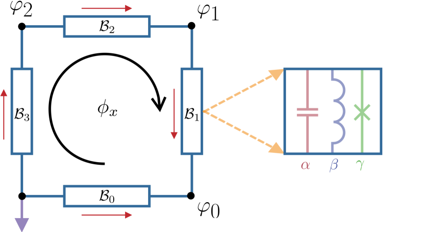
Genetic algorithms are heuristic optimization algorithms inspired by Darwinian selection. In our problem, the individuals correspond to circuit configurations consisting of single or multi-loop elements as depicted in Fig. 1. Different circuit elements lead to distinct individuals. As we aim at engineering architectures satisfying specific energy spectrums with given selection rules, these individuals are evaluated and scored depending on how well they craved the required conditions through the cost function. To find the optimal circuit, a crucial step relies on automatizing the circuit quantization method to compute each individual’s spectrum and transition element. In the first part of this section, we focus on developing the tools to perform this automatic diagonalization.
Let us consider a single-loop circuit with four links, each containing randomly chosen elements among capacitors, inductors, Josephson junctions, or just their absence. The general configuration of the loop has associated a parallel-connected non-linear circuit to each link , see Fig. 1. In this derivation, we have assumed that all the values of the circuit parameters are fixed. The th link is characterized by the array that contains all the information about which circuit element corresponds to that link. Thus, the parameters correspond to binary numbers having as entries, such that only one of them is equal to one and the others are zero. For example, the set refers to the th link as a capacitor, whereas the configuration refers to the link absence (wired connection), respectively.
In order to avoid superfluous variables describing the circuit, we represent its Lagrangian in terms of the nodes variables [39], which can be conveniently expressed as the following quadratic form
| (1) | |||||
Here, is the magnetic quantum flux, with beings the electric charge, moreover, corresponds to the phase variable vector describing the th node. Furthermore, and are the capacitance and the inverse of the inductance matrix
| (5) | |||||
| (9) |
where, is the equivalent capacitance of the th branch. Moreover, is the equivalent inductance, where , and represent the capacitance, inductance, Josephson capacitance and Josephson energy of the th element.
Notice that it is possible to manipulate the properties of the electrical circuit by threading it with an external magnetic flux . In our Lagrangian, such dependence appears through the fluxoid quantization rule. In our work, we follow the same approach as in Ref. [41], in which they choose the closure branch where a Josephson junction is placed. In other words, for the array that contains all the information about the Josephson junction in the circuit, we choose any and add to the corresponding phase difference. In order to automatize this procedure on our algorithm, we select the closure branch as the first one that satisfies . In our particular case, without loss of generality, we choose the branch “0” to apply the fluxoid quantization rule. Thus, the circuit Lagrangian modifies as follows
| (10) | |||||
Within this approach, it is possible to design several circuit configurations simply by changing the parameters , , and , respectively. However, we need to discriminate the circuit configurations that may lead to circuits without quantum Hamiltonian as in the case of single-loops containing only capacitors or inductors, respectively. Furthermore, within these configurations, there exist circuits having passive nodes where two or mode inductors (capacitors) converge [39]. In this situation, the circuit will contain more coordinates (velocities) than velocities (coordinates), and these energy terms on the Lagrangian correspond to free particles [71]. We can eliminate these terms through the Euler-Lagrange equation . For the case where a coordinate (velocity) is missing, we obtain that (). This condition permits us to write the passive node in terms of the active ones. Notice that this procedure is equivalent to calculating the effective inductance (capacitance) on this node. For a detailed explanation of passive node elimination, see Appendix A.
Until here, we obtain a circuit Lagrangian that lacks a superfluous variable since the fluxoid quantization rule and the elimination of the passive nodes. We proceed to calculate the circuit Hamiltonian using the Legendre transformation, obtaining
| (11) | |||||
where is the inductive energy matrix. Notice that in superconducting quantum circuits, the electrical charge is proportional to the number of Cooper-pairs on the device. In this way, we can define , where is the vector describing the number of Cooper-pair associated with each superconducting phase . In this representation, we write the circuit Hamiltonian as follows
| (12) | |||||
where is the charge energy matrix.
To engineer an electrical circuit that meets desirable specifications, we define a cost function that evaluates all possible candidates to qualify them according to how likely the device fulfills the specifications. This cost function takes as input the set that encodes the circuit topology, and the set that the determines the working regime of the device and provides a real number whose minimum is the craved circuit. In this work, we will first find the optimal circuit topology by fixing the set of circuital parameters (including the external flux). The latter constitutes our minimization unit. Once we find the optimal circuit topology, we search for the optimal set . The resulting circuit satisfies the desired energy spectrum and transition matrix elements.
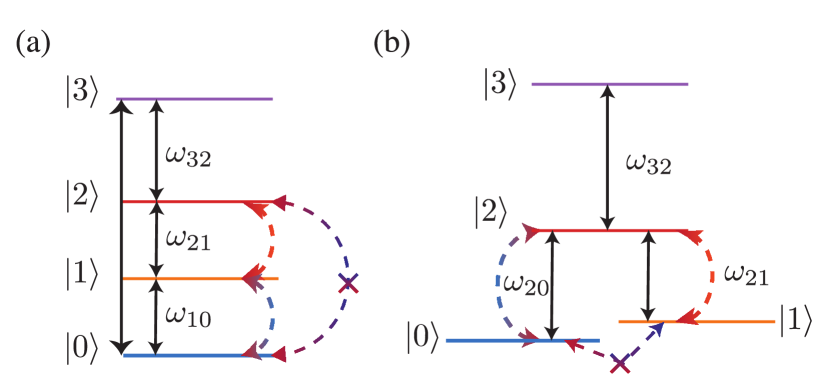
In our work, we use our automatized circuit quantization method to find the optimal configuration and circuital parameters such that the device works effectively as an atomic system. Here, we will focus on designs a ladder () and lambda () three-level system. For the former, we require that the first two-energy transitions and be identical, here is difference between the th and the th energy level of the device described by the circuit Hamiltonian. Moreover, to avoid population leakage to higher energy levels, we also demand that the transition be out of resonance from and , as depicted in Fig. 2(a). Finally, to ensure that the energy spectrum is consistent with the experimental implementation of the platform, we bound the low-lying energy spectrum up to a frequency cut-off [20, 72, 23]. We encode these requirements as follows
| (13) |
here, is a control parameter (with units of frequency) that fix the detuning between the transitions , and , respectively. On the other hand, we also require engineering the set of transitions allowed for the device, particularly for the ladder system we demand transitions between adjacent energy levels, such as the states and , and we forbid transitions involving two-photon processes as [49], where is the th eigenstate of the system. In this direction, we may impose some constrain on the transition matrix elements of the device through the differences
| (14) |
where corresponds to a particular operator of the electrical circuit. For instance, we will use the charge operator for our calculations.
Therefore, a good choice for the cost function corresponds to the hypersphere . We apply the same reasoning to define the needed conditions to design a lambda system. Contrary to the ladder, this architecture requires two metastable ground states. Thus, the low-lying energy state of the device should be degenerate, imposing that . We also demand that these metastable states have equal energy transitions with the first excited state. In other words, we need that , see Fig. 2(b). These conditions are determined by the differences
| (15) |
It is worthwhile noticing that we do not impose the condition to be out of resonance from and to avoid access to higher energy levels. Nonetheless, we will prove later that state does not show up in the system dynamics. Besides, the set of transitions for the lambda system requires no interaction between the two metastable states , and only interactions mediated by the first excited state are allowed, i.e., and [50, 49]. These conditions are summarized in the following differences
| (16) |
Hence, we define the cost function as . Thus, a minimal value of our cost functions will correspond to electrical circuits satisfying the circuit’s required spectral and dynamical properties. We carried out the findings of those circuits through two minimization processes. The first one finds the optimal set that encodes the circuit topology. Here it is convenient to use algorithms that deal with a discrete set since the topology corresponds to arrays of binary numbers. The second minimization relies upon finding the operating regime of the circuit. In other words, we may reach the optimal set so that the device’s spectral and dynamical properties satisfy our requirements and its circuital values be consistent with experimental realization within the quantum platform. This minimization searched the optimal over a continuous set of parameters bounded by the values , , , and [73, 72, 32, 74].
We will find both the optimal topology () and circuital parameters () using the Genetic Algorithms [6]. For the topology minimization, we start by defining a set of circuits with different topologies consisting of our initial population, and we proceed by calculating the cost function of each of them. In this stage, we may select configurations that are the circuits with the highest fitness or the smallest cost function. We term this subset as parents, mixing them to generate different circuit configurations or the offspring. We implement the mixing by selecting the circuits according to their active nodes and merging them to generate a new circuit. Furthermore, we will consider the newborn an invalid configuration if it only contains capacitors or inductors. In that case, it is impossible to define a quantum Hamiltonian because of the lack of one of the canonical conjugate variables (phase or charge), and we repeat the process until we generate a valid configuration. Then, we check if the new circuit contains passive modes to eliminate it following the same procedure described in Appendix. We reiterate this process times since we require that the size of the population never change during the minimization process. All the merging procedure is termed as crossover. To avoid the cost function being trapped on a local minimum, we add to the system mutations corresponding randomly select an individual of the new population and change one of its circuital elements; for example, we may change an inductor for either a Josephson junction or a capacitor.
The use of minimization subroutines rather than brute force search relies on the size of the space parameter. The circuit topology space for a single loop contains possible configurations; however, several of them lead to circuits with no Hamiltonian. For instance, electrical circuits with only capacitors or inductors in all links lack a Hamiltonian. We eliminate these configurations from the set, obtaining a parameter space for the single-loop circuit to be , where is the combinatorial symbol. For the one-dimensional array having sites, as the depicted in Fig. 3, the number of combination scales as , respectively.
The optimization of the circuital parameter space works as follows. For a fixed topology, , we define a set of arrays containing different circuit values (add set). Then, we calculate the cost function of each of them and select configurations with the lowest cost function value. We create the offspring by dividing the parent arrays and concatenating them so that the new layout does not change its size. Again, we repeat this procedure times to obtain the new population. We implement the mutation by randomly selecting an element of the new population’s array and changing its values randomly. This optimization is computationally less demanding than the topology ones since the circuital parameter space for a single-loop circuit has dimension eight at most, corresponding to a device with four Josephson junctions. Other single-loop configurations will have fewer parameters. Thus, for a one-dimensional array having sites, the number of parameters scales as . In 1 we have written a pseudo-code of our algorithm.
In our simulations, we selected 16 random circuits as the initial population for the topology optimization. On the other hand, for the multi-loop circuit, we have chosen 16 random arrays of different combinations of the optimal circuit arrangement obtained during the single-loop optimization. For both minimization, we have used a mutation probability of .
III Automatized circuit quantization
Thus far, we have described how to engineer the topology and choose the adequate circuital parameters using a bio-inspired algorithm such that the resulting electrical circuit satisfies the same energy spectrum and selection rules as atomic three-level systems. The genetic algorithm proposed here requires the Hamiltonian matrix representation to compute the previously defined cost function. Thus, choosing the correct quantization basis is mandatory so that the electrical circuits encompass all the underlying physics. The starting point of our automatized circuit quantization method is the classical Hamiltonian given in Eq. (12)
We obtain the quantum Hamiltonian by promoting the number of Cooper-pair and phase variables as quantum operators satisfying canonical commutation relation. In our work, the circuit topology strongly biases the quantization basis for each node operator; for devices only having capacitors and Josephson junctions, we call them Cooper-pair-box-like configurations. In this case, is a diagonal operator, and the cosine term represents tunneling of Cooper pairs, and they are expressed in terms of which satisfy the canonical commutation relations in the form . On the other hand, it is also possible that our circuit provides configurations only having capacitors and inductors or capacitors, inductors, and Josephson junctions as the case of the Fluxonium circuit [77]. In these cases, the quantization basis corresponds to the Fock basis where we define annihilation and creation bosonic operators and that satisfy the commutation relation .
To automatize the selection of the quantization basis for each node, we have to look more in depth at the potential term of the circuit Hamiltonian in Eq. 12. For this analysis, we expand the potential up to the fourth order in the phases ()
| (17) | |||||
advert that the expansion coefficients are functions of the Josephson energies. Afterward, we calculate the second and fourth order derivative of the expanded potential with respect to , as an example, we will consider the phase
| (18) | |||||
where is the matrix element of the inductance energy matrix. From the equations Eq. (18) and Eq. (III) it is possible to define the criteria to choose the charge or the oscillator basis quantization. If vanishes, but does not it means that there is no cosine potential associated with node variable . Consequently, we quantize the phase and its corresponding charge using the annihilation and creation operator of the quantum harmonic oscillator. On the contrary, we may think that if and are not zero, the node variable could be quantized in terms of the charge basis. However, this is not in general true. For instance, a fluxonium-like configuration consisting of capacitors, inductance, and Josephson junctions fulfills the above-mentioned conditions. However, this architecture is usually quantized in terms of annihilation and creation bosonic operators. To circumvent this problem, we add the constraint , meaning that the th branches have not associated inductance and consequently. If a given node meets these three conditions, we quantize this degree of freedom using the charge basis. This procedure allows us to automatize the quantization basis of each node using physical arguments regarding in the presence/absence of Josephson junction and inductors on the electrical circuits. We repeat this procedure for all the active nodes on the circuit.
For a circuit only containing capacitors and inductors, our automatized method for choosing the quantization basis leads to the following quantum Hamiltonian
| (20) |
this Hamiltonian describes a set of coupled harmonic oscillators that can be quantized using the operators and defined in terms of annihilation and creation bosonic oscillator as
Here, , and are the diagonal elements of the charge and inductive matrix, respectively. These operators satisfy canonical commutation relations that leads to the Hamiltonian of single-loop circuit ()
where , and correspond to the oscillator frequency, capacitive and inductive coupling strength given by
| (21a) | |||||
| (21b) | |||||
| (21c) | |||||
On the other hand, for a circuit with two nodes only containing capacitors and Josephson junctions, the automatized method gives us the following circuit Hamiltonian
| (22) | |||||
In the charge basis, the and cosine operators are expressed in the following form
| (23) |
These operators satisfies the canonical commutation relation . The quantum circuit Hamiltonian reads
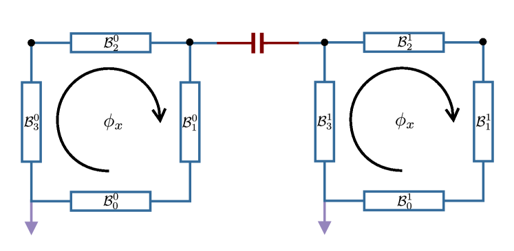
We extend the analysis to a one-dimensional array of single-loop capacitive connected to each other, see Fig. 3, described through the Hamiltonian
| (25) |
where is the single-loop Hamiltonian in Eq. (11) for each loop. Furthermore, each site is coupled with a capacitor with strength , where is the coupling capacitance. Moreover, and corresponds to the charge operators of the th and th single-loop boxes. The exact diagonalization of Hamiltonian (25) is a difficult task, even for small-size one-dimensional arrays. The dimension of the Hilbert space exponentially scales with both the number of sites and the number of degrees of freedom of each single loop circuit. Algorithm 2 shows the automatized circuit quantization subroutine.
IV Optimal circuit configuration
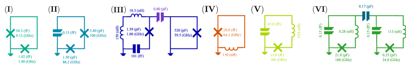
We analyze the resulting circuits obtained by minimizing the cost function provided in the previous section. Here, we will focus on the ladder () and lambda () configuration containing two and three links and then extend to an architecture consisting of two coupled single-loop circuits as depicted in Fig. 3. The circuit topology, circuital parameters, and the energy transition of each optimal circuit for the ladder and lambda three-level system are summarized in tables 1 and 2, respectively. Whereas we provide a graphical illustration of them in Fig. 12.
|
|
||||||||
| I | ||||||||
| 0 | 0 | 0 | 1 | 0 | 0 | 0.00192 | 1.000 | |
| 1 | 0 | 0 | 0 | 0 | 0 | 0 | 0 | |
| 2 | 0 | 0 | 0 | 0 | 0 | |||
| 3 | 0 | 0 | 1 | 0 | 0 | 0.0542 | 9.127 | |
| II | ||||||||
| 0 | 0 | 0 | 1 | 0 | 0 | 1.50 | 88.2 | |
| 1 | 0 | 0 | 1 | 0 | 0 | 3.403 | 100 | |
| 2 | 0 | 0 | 0 | 0 | 0 | 0 | 0 | |
| 3 | 1 | 0 | 0 | 0.00015 | 0 | 0 | 0 | |
| III | ||||||||
| Box 1 | ||||||||
| 0 | 1 | 0 | 0 | 0.101 | 0 | 0 | 0 | |
| 1 | 0 | 0 | 1 | 0 | 0 | 1.59 | 1 | |
| 2 | 0 | 1 | 0 | 0 | 18.25 | 0 | 0 | |
| 3 | 0 | 1 | 0 | 0 | 150 | 0 | ||
| Box 2 | ||||||||
| 0 | 0 | 0 | 0 | 0 | 0 | 0 | 0 | |
| 1 | 0 | 0 | 0 | 0 | 0 | 0 | 0 | |
| 2 | 0 | 0 | 1 | 0 | 0 | 0.52 | 59.45 | |
| 3 | 0 | 0 | 0 | 0 | 0 | 0 | 0 | |
| Coupling | ||||||||
| 0 | 1 | 0 | 0 | 0.803 | 0 | 0 | 0 | |
| System parameters | ||||||||
| I | 4.90 [GHz] | 4.47 [GHz] | 4.06 [GHz] | 13.43 [GHz] | ||||
| II | 3.53 [GHz] | 5.22 [GHz] | 7.04 [GHz] | 15.8 [GHz] | ||||
| III | 2.09 [GHz] | 2.44 [GHz] | 0.61 [GHz] | 5.15 [GHz] | ||||
|
|
||||||||
| IV | ||||||||
| 0 | 0 | 1 | 0 | 0 | 150 | 0 | 0 | |
| 1 | 0 | 0 | 0 | 0 | 0 | 0 | 0 | |
| 2 | 0 | 0 | 0 | 0 | 0 | 0 | 0 | |
| 3 | 0 | 0 | 1 | 0 | 0 | 0.028 | 64.21 | |
| V | ||||||||
| 0 | 0 | 0 | 1 | 0 | 0 | 0.015 | 100 | |
| 1 | 0 | 1 | 0 | 0 | 19.84 | 0 | 0 | |
| 2 | 0 | 0 | 0 | 0 | 0 | 0 | 0 | |
| 3 | 1 | 0 | 0 | 0.045 | 0 | 0 | 0 | |
| VI | ||||||||
| Box 1 | ||||||||
| 0 | 0 | 0 | 1 | 0 | 0 | 0.0021 | 100 | |
| 1 | 0 | 1 | 0 | 0 | 0.24 | 0 | 0 | |
| 2 | 0 | 0 | 0 | 0 | 0 | 0 | 0 | |
| 3 | 1 | 0 | 0 | 0.00015 | 0 | 0 | 0 | |
| Box 2 | ||||||||
| 0 | 0 | 0 | 1 | 0 | 0 | 0.356 | 34.28 | |
| 1 | 0 | 1 | 0 | 0 | 113 | 0 | 0 | |
| 2 | 0 | 0 | 0 | 0 | 0 | 0 | 0 | |
| 3 | 1 | 0 | 0 | 0.00015 | 0 | 0 | 0 | |
| Coupling | ||||||||
| 0 | 1 | 0 | 0 | 0.173 | 0 | 0 | 0 | |
| System parameters | ||||||||
| IV | 0 [GHz] | 18.27 [GHz] | 18.27 [GHz] | 18.27 [GHz] | ||||
| V | 0 [GHz] | 5.07 [GHz] | 5.07 [GHz] | 5.07 [GHz] | ||||
| VI | 0 [GHz] | 13.3 [GHz] | 13.3 [GHz] | 15.9 [GHz] | ||||
Table 1 shows that the optimal configuration for a three-level system consisting of two links (I) corresponds to a pair of coupled Josephson junctions threaded by an external magnetic flux. Notice that this configuration is similar to the split-transmon circuit or the Rf-SQUID [75, 76] architecture corresponding to archetypal charge and flux qubit, respectively. In these systems, the low-lying energy spectrum has large anharmonicity that guarantees to perform logic operations on them. Furthermore, their charge operators follow the same selection rules as a three-level system. Moreover, the minimization algorithm extends the previous result for a single-loop device consisting of three links (II); the optimal circuit corresponds to a pair of Josephson junctions coupled to a capacitor. In this architecture, the additional capacitor changes the ratio between the total Josephson energy with the respective charge energy, similar to the transmon circuit. In such a device, the charge operator also demonstrates the same selection rules as the three-level system. Finally, for the extended circuit (III), the optimal architecture corresponds to the capacitive coupling between a single-Josephson junction with a circuit consisting of two inductors connected to a capacitor and an additional Josephson junction.
On the other hand, for the three-level system that consists of a single-loop circuit with two links (IV), the optimal architecture is like a Fluxonium configuration [77] formed by a Josephson junction coupled to an inductor. Notice that this configuration behaves as a three-level system for an external magnetic flux fixed at [50]. Like the three-level system, we obtain that the optimal circuit configuration having three links (V) is the extension of the previous one, where we couple an additional capacitor to the Josephson junction and the inductor, respectively. Finally, the optimal configuration for an extended circuit (VI) corresponds to a pair of Fluxonium coupled capacitively with each other. As expected, our circuital parameters are consistent with the reported values in the previous cQED implementations.
To compare the performance of each optimal circuit architecture, we will calculate at zero external flux, the energy differences and the relative anharmonicity between the low-lying energy spectrum defined as , with the transition frequency between the th and th energy states, respectively. Let us start with the three-level system
| (26a) | |||||
| (26b) | |||||
For circuit (I), we obtain similar values for the anharmonicity. These results confirm that the device behaves as a split transmon circuit since the first three lowest energy transitions are identical. Consequently, we can model the device as a weakly anharmonic oscillator. Moreover, we obtain significantly larger anharmonicity for the second circuit (II) than the device (I), respectively. Each device’s successive energy transitions are different, making it unsuitable for the required three-level system. Finally, we achieve better performance for the extended multi-loop circuit (III) than the other two configurations. We obtain a low anharmonicity between the first and the second excited state , whereas the third energy level off-resonance from the two different low-lying energy levels . Thus, the extended multi-loop circuit attains the required spectral configuration for the three-level system.
We extend a similar analysis for the configuration. However, instead of calculating the anharmonicity implying the first energy transition, we consider the energy differences mediated by the second excited state as and . Moreover, as pointed out in Table 2, we obtain that for the lambda circuits containing two (IV) and three links (V), respectively. The relative anharmonicity is zero, which corresponds to a quantum system with a degenerate ground state. Notice that this degeneracy also appears on the second and third excited states where the relative anharmonicity is zero. That condition makes it unsuitable for a lambda configuration since it is very likely that these degenerate energy states will participate in the system dynamics. For the extended multi-loop configuration, we obtain that the relative anharmonicity between the transitions and is also zero. Nevertheless, the one-dimensional array breaks the degeneracy between the second and the third excited state, obtaining a relative anharmonicity that permit to avoid the dynamics involving higher excited energy levels.
We conclude that, in multi-loop circuits (III and VI), our algorithm finds architectures with better performance in comparison with the single-loop circuit having two and three links each. We attribute such improvement to the presence of redundancy that involves having several degrees of freedom on the device. This over plus creates manifolds whose energy spectrum is robust against fluctuations in the physical parameters leading to noise protection [78]. However, we may not conclude that this enhancement will always occur because our algorithm only relies on a single value of the frustration parameter . The complete analyses must be done by varying the frustration parameter and exploring the behavior of both the energy spectrum and the transition matrix elements to conclude the robustness of the multi-loop circuits.
V Dependence on the external magnetic flux
The next step in the characterization of the optimal device obtained with our algorithm relies on its response (tunability) of the energy spectrum and transition matrix elements of the charge operator when an external phase thread either the single-loop or the extended one-dimensional array. Here, we consider the number operator at the edges of both configurations (the single-loop and the extended one-dimensional system). Moreover, we use a linear modulation for the external phase of the form .
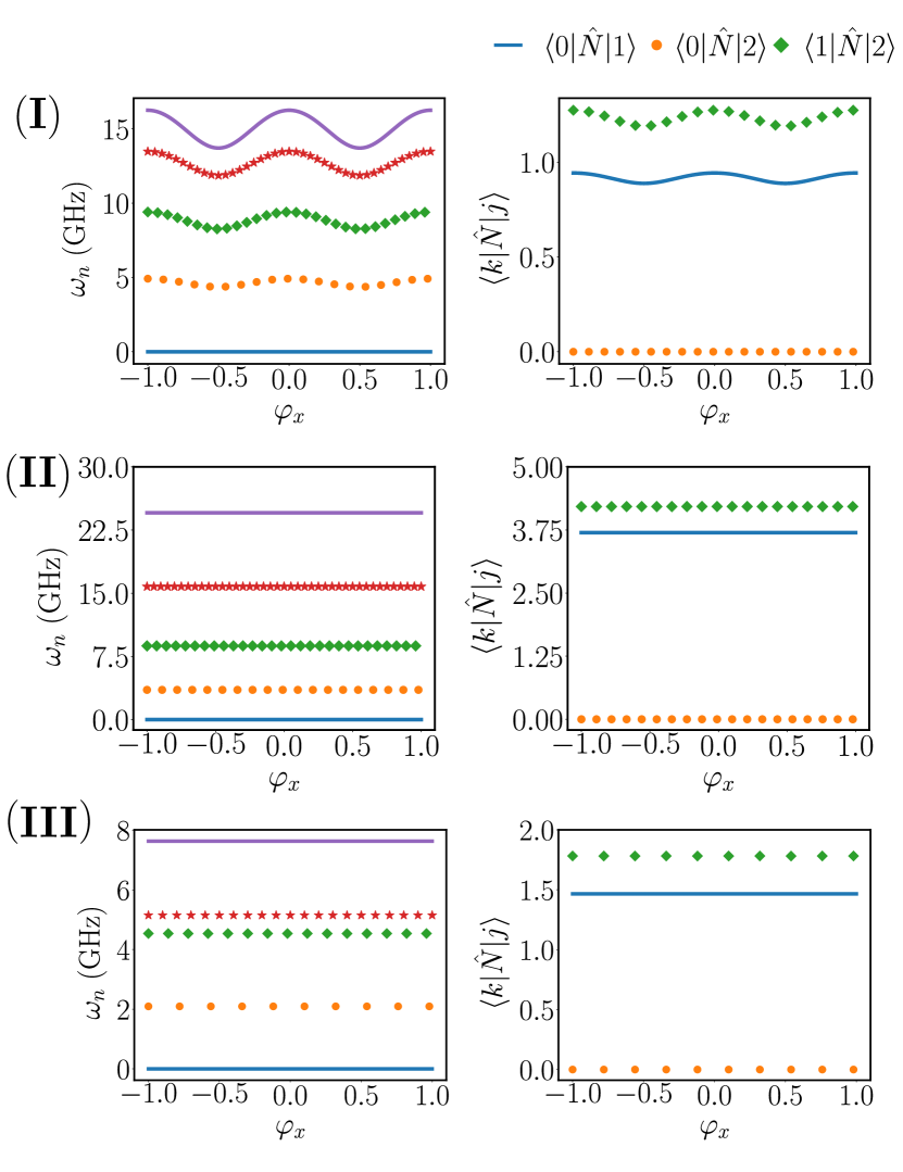
Figure 4 depicts the low-lying energy spectrum and the transition matrix elements [, , ] for the single-loop circuit containing two links (I), three links (II), and the multi-loop linear array (III), respectively. For the device (I), we observe that the studied quantities changes with the external flux exhibiting an oscillatory behavior. Nevertheless, the changes are sufficiently small not to appreciate avoided energy spectrum. Moreover, as pointed out in the previous section, we also see low anharmonicity between the successive energy levels. We also see that the transition matrix elements satisfy the requirement for a three-level system where the transition is highly suppressed since its matrix element is always zero. Also, the transition matrix elements , and slightly oscillate, guaranteeing transitions between consecutive energy levels.
We see the absence of such oscillations in the low-lying energy spectrum and transition matrix elements for the three-links circuit (II) and the multi-loop device (III). In other words, the studied quantities become insensitive to fluctuations in the control parameter, as depicted in Fig. 4 (II) and Fig. 4 (III), respectively. These architectures also satisfy the conditions to behave as a three-level system where the matrix element is suppressed.
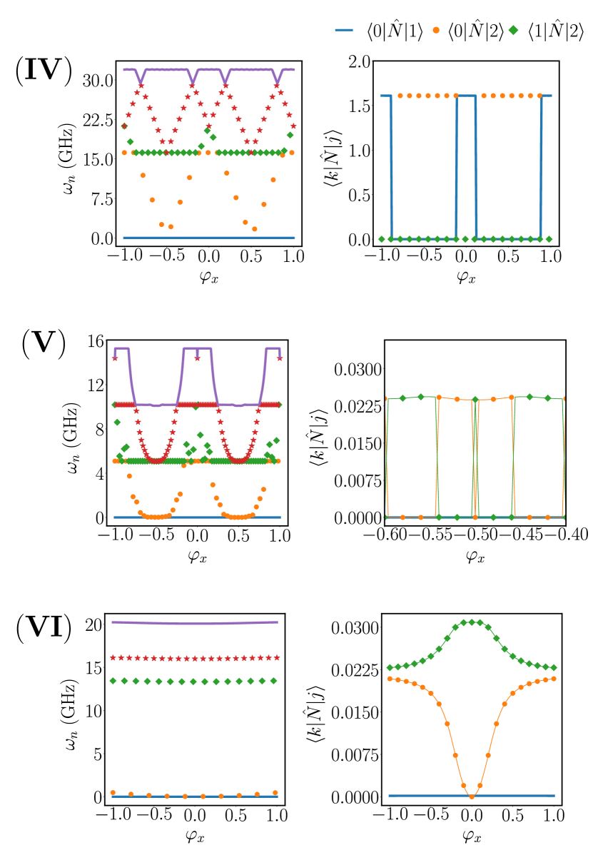
We extend the same analysis to the optimal architecture for the system. Fig. 5 shows the low-lying energy spectrum and the transition matrix elements (, ,) for a single-loop having two and three links, as well as the multi-loop configuration.
For both single-loop circuits (VI) and (V), we observe that the low-lying energy spectrum and the transition matrix elements present sweet spots around . At this value, the first two energy levels mutually approach (), forming quasi-metastable energy levels, as depicted in Fig. 5. At these values, the relevant transition matrix elements satisfy the desired criteria at these values where the transition matrix element vanishes, as shown in Fig. 5.
Finally, we consider the multi-loop with the parameters from Table 2. For this architecture, the energy spectrum becomes quasi-insensitive to the frustration parameter. Even though the energy spectrum of the artificial atom changes with , its energy differences remain constants (see panel (VI) from Fig. 5). Moreover, the relevant transition matrix element of both charge and flux operator vanishes at . For another value of the frustration parameter. The system does not behave as a three-level system; for other values of the external magnetic flux, the transition matrix elements satisfy , and .
We conclude that, for circuits containing a single quantum degree of freedom (I and IV), it is hard for the algorithm to find a suitable architecture in which both the atomic energy spectrum and its correspondent selection rules are attained. We can only obtain sweet spots where the system mimics the atomic system. In contrast to circuits with fewer degrees of freedom, those with more offer a wealth of potential parameter configurations. This can manifest as spectral manifolds or protected subspaces [78, 79], enabling the design of circuits with specific spectral characteristics and selection rules. Additionally, the added redundancy in the degrees of freedom makes these circuits more resilient, allowing for ’sweet regions’ of operation in which the circuit behaves in a way that is similar to an atomic system.
VI Dynamical properties
We study the dynamics of the optimal circuits under the action of a driving tuned to the relevant transition acting on the charge operator described by the Hamiltonian of the system reads
| (27) |
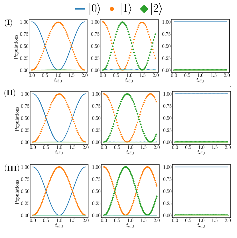
where is the Hamiltonian of the optimal single-loop and multi-loop configuration obtained in Table 1 and Table 2, moreover, is the driving strength, and corresponds to the driving frequency, which we have selected to be , or . We calculate the probability evolution of the eigenstates of by initializing the system in its ground state for the driving frequencies and , whereas we initialize the system and in for , respectively.
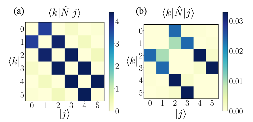
Figure 6 shows the population evolution for the circuits (I), (II) and (III) biasing , in units of the dimensionless time , where corresponds to the transition matrix element for the node charge operator.
From a dynamical point of view, we see that every circuit configuration found by our algorithm behaves as three-level system; depending on the driving frequency, the device access to adjacent energy states , and without inducing transitions involving additional higher excited energy levels. In fact, for panel (I) regarding the single-mode circuit, the population trapped in the second excited state is negligible in comparison with the population in the first excited state, observing an almost-complete Rabi oscillation between the states . For multi-loop circuits (panel (III)), we observe that the higher energy transitions are suppressed, obtaining Rabi oscillations between the adjacent levels. We understand this by looking at Fig. 8 where we have plotted the transition matrix element for the phase and charge operator for the circuit (III), observing that the dominant transition matrix element corresponds to the adjacent states and . In this scenario, transition involving more than one excitation is suppressed because it corresponds to a slow process that will not occur within the addressing time scale provided by the driving. Another reason for obtaining the system dynamics in a reduced Hilbert space relies on the anharmonicity between the excited energy levels.
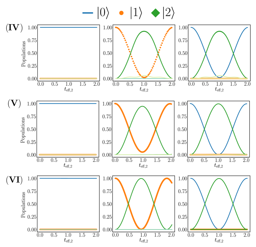
We extend the same analysis to the configuration showing the system dynamics of the circuits (IV), (V) and (VI) in Fig. 7. We observe a poor performance for the single-mode circuits from a dynamic point of view. Even though it is possible to suppress the transition (there is no evolution of the probability), we observe population leakage and trapping in the higher excited energy states. Consequently, we see an imperfect Rabi oscillation between the resonance eigenstates. We appreciate the absence of trapping and leakage in the higher energy states for the multi-loop circuit as depicted in Fig. 8(VI). Thus, the redundancy in terms of the degree of freedom allows us to design architectures achieving both the desired energy spectrum and the dynamic properties of an atomic system.
VII Resilience against circuit parameter fluctuations
We evaluate the robustness of our protocol against parameter fluctuation on their circuital parameters. We will focus on the multi-loop cases, which have demonstrated better performances than the single-mode configurations. We start with controlled errors in one of the capacitors and then extend to all the parameters. Finally, we analyze the performance of the multi-loop architecture in which all parameters fluctuate.
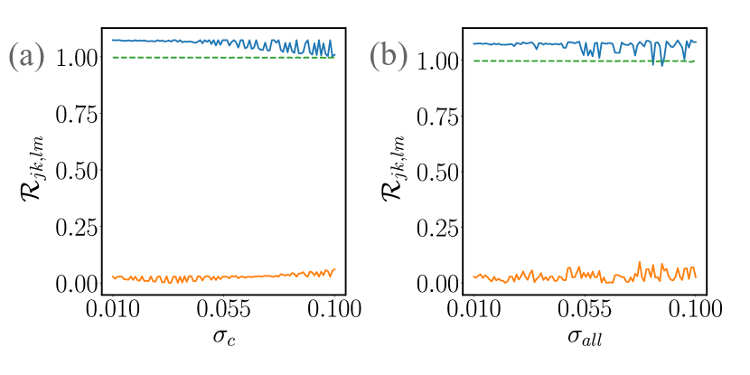
For the controlled errors, we assume random deviations around of the optimal parameters obtained in Table 1, and Table 2 for the multi-loop case, respectively. For all the parameters fluctuating, we consider a normal distribution of the optimal parameters with a deviation of around the optimal values. We evaluate the performance of the multi-loop circuit in terms of its energy transition through the following ratio.
| (28) |
Where is the th transition of the multi-loop circuit. For an ideal three-level system, we expect meaning that the energy transitions and have identical transition frequencies. Moreover, we also demand that that characterize the discrepancy between the energy transitions and such that the former be not accessible during the dynamics. Notice that could be larger or smaller than one depending on which energy transition has a larger transition frequency. Contrary, for an ideal three-level system, we demand that , which means that the energy transitions and are similar.
Figure. 9(a) shows the set of ratios , , and as a function of the capacitance error , whereas Fig. 9(b) show them as a function of the total error , respectively. The figures show that both multi-loop three-level systems are resilient against these controlled parameter errors. The three-level system depicts that the ratio has a stable value for small controlled errors (). In contrast, it shows larger fluctuations around for controlled errors which are larger than this value. However, even though these fluctuations are noticeable, they converge to , which is the condition needed for a good three-level system. For the ratio , we observe fluctuations around zero, ensuring that the adjacent energy transition and its respective matrix elements of the three-level system keeps the same structure with similar transition frequencies also being far off-resonance with higher energy transitions.
We extend the discussion for the multi-loop three-level system, also showed in Fig. 9(a)-(b). The figure shows that this architecture is more resilient against controlled errors since the ratio keeps a constant value around one for all the analyzed ranges. Then, our automated circuit quantization algorithm gives us a set of three-level systems with optimal circuit architecture resilient against controlled fluctuation on the circuital parameters.
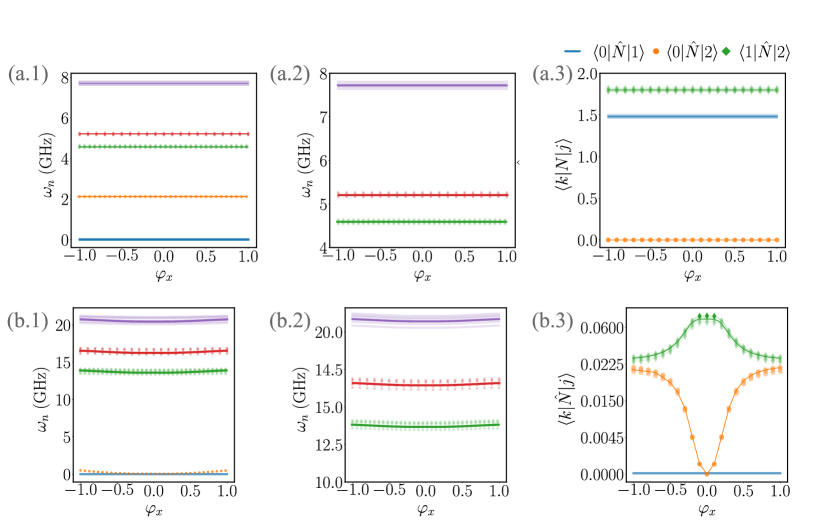
We provide additional evidence of resilience against fluctuations by calculating the energy spectrum and the transition matrix element of both optimal circuits (III) and (VI). We consider a data set of 100 samples whose parameters follow a normal distribution averaged with the parameters obtained in Table 1, and Table 2 with deviations around . We summarize our findings in Fig. 10, where we have plotted the energy spectrum and the transition matrix elements for all those configurations.
For the multi-loop three-level system, Fig. 10(a.1) shows that the first two energy levels are more resilient against fluctuations since these energy transitions are almost constant for all the circuits of the dataset. The effect of the deviations appears from the second excited state, where the energies oscillate around an equilibrium configuration consisting of the average of these transitions without changing the anharmonicity of these states as depicted in Fig. 10(a.2) where we show an inline of Fig. 10(a.1) with the highest energy levels that confirm our statement. For the transition matrix elements, we appreciate that it follows the exact behavior of the low-lying energy levels; the values fluctuate around the average, but still, the circuit maintains the selection rules imposed by the algorithm, see Fig. 10(a.3).
For the multi-loop three-level system, we observe a similar tendency to the ladder three-level system. The first two energy levels are resilient against fluctuations because they are constant for all the circuits of the dataset for all the values of the control parameter. Only for the highest energy levels can we observe the effects of the deviations. See Fig. 10(b.1) and the inline depicted in Fig. 10(b.2). Finally, for the transition matrix elements, we appreciate that it follows the exact behavior of the low-lying energy levels.
In conclusion, the multi-loop three-level system performs better against controlled errors since it does not exhibit appreciable changes in the figure-of-merit used to quantify its resilience. On the contrary, we observe larger fluctuations for the three-level system, but they converge to the expected value.
For the random sampling of the circuit parameters, we observe identical performance for both multi-mode circuits; the fluctuations in the energy levels start to appear in the second excited state of both configurations. Nevertheless, changes on the spectrum do not modify the anharmonicity between them since they all happen in the same proportion for deviations around 5. We observe similar behavior for the transition matrix elements, where the presence of the fluctuations does not alter the selection rules of the multi-loop configuration. Thus, designing architectures with engineered energy levels and selection rules within consistent cQED parameters with bounded fabrication errors is possible.
Conclusions
In this work, we have used genetic algorithms to design superconducting quantum circuits with atomic energy spectra and selection rules mimicking ladder and lambda three-level systems. The algorithm starts by developing an automatized circuit quantization subroutine to calculate the quantum Hamiltonian of a multi-loop system composed of randomly selected circuit elements. Our approach can choose an adequate quantization basis for each degree of freedom constituting the multi-loop system relying upon the circuit configuration. Then, the genetic algorithm adapts the circuit topology and the circuital parameters so that its energy spectrum and transition matrix elements behave as desired, i.e. as a specific three-level system.
We have found that in single-loop configurations, there exists a tradeoff between attaining the spectral requirement of the circuit and meeting the desirable conditions for the transition matrix elements. The conclusion is that the system has too few free parameters to fulfill all conditions simultaneously. We circumvent this problem by using a multi-loop system comprising two single-loop systems. With this setup, we have obtained that it is possible to satisfy all the conditions for a wide range of the control parameter named sweet regions. Additionally, we demonstrated that our multi-loop circuits are robust against random fluctuations in their circuit parameters, such as fabrication errors, making them suitable for use in large-scale setups as modular components with specific symmetries.
ACKNOWLEDGEMENT
F. A. C. L acknowledges F. Motzoi and E. Solano for helpful discussions. The authors acknowledge support from the German Ministry for Education and Research, under QSolid, Grant no. 13N16149, the Chilean Government Financiamiento Basal para Centros Científicos y Tecnológicos de Excelencia (Grant No. FB0807), USA2055_DICYT, Universidad de Santiago de Chile. The also acknowledge financial support from the Basque Government through Grant No. IT1470-22 and from the Basque Government QUANTEK project under the ELKARTEK program (KK-2021/00070), the Spanish Ramón y Cajal Grant No. RYC-2020-030503-I and No. RYC-2017-22482-I, and project Grant No. PID2021-125823NA-I00 funded by MCIN/AEI/10.13039/501100011033 and by “ERDF A way of making Europe” and “ERDF Invest in your Future”, as well as from OpenSuperQ (820363) of the EU Flagship on Quantum Technologies, and the EU FET-Open projects Quromorphic (828826) and EPIQUS (899368).
Appendix A Eliminating passive nodes
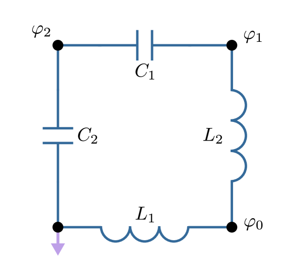
In this section, we illustrate how to eliminate the passive nodes present in a random configuration of the single loop. For doing so, let us consider the circuit depicted in Fig. (11) whose Lagrangian reads
| (29) | |||||
As no Josephson junction exists in this configuration, we do not apply the fluxoid quantization rule. Afterward, we calculate the Euler-Lagrange equations for all the node variables present in the configuration, obtaining
From these equations, it is easy to note that some generalized coordinates and velocities are missing. In particular, Eq. (30) lacks generalized velocity, and Eq. (30) misses the generalized coordinate. These variables constitute the passive nodes of the circuit, and we can eliminate them by solving the non-zero part of the Euler-Lagrange equation in terms of the active node, namely , obtaining
| (31a) | |||||
| (31b) | |||||
We obtain the circuit Lagrangian without passive nodes just by replacing Eq. (31a) and Eq. (31b) in the Lagrangian in Eq. (29)
| (32) |
Notice that now, the circuit Lagrangian is described by a single degree of freedom that corresponds to an LC circuit with effective capacitance and inductance, respectively.
Now, both kinetic and inductive terms contain the same variables. Notice that this Lagrangian is the same as considering a circuit with only one inductance with a value equal to the effective inductance of the passive node.
Appendix B Numerical Convergence of the Single loop circuit
In this section, we perform a numerical analysis concerning the energy spectrum of the single-loop Hamiltonian given in Eq. (III). We focus on two aspects; the convergence of Hilbert space describing the single loop circuit Hamiltonian and how the non-linear terms change the anharmonicity in the energy spectrum.
B.1 Optimal Hilbert space size
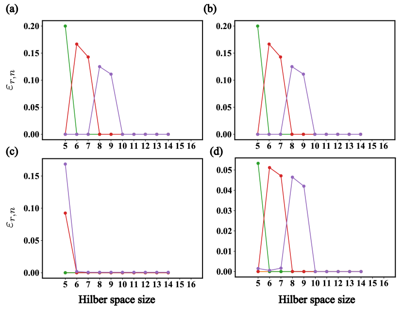
We compute the energy spectrum of the harmonic part of Hamiltonian from Eq. (III), and we diagonalize it by increasing the Hilbert space by adding one excitation on each mode. Then, we compare the th energy level for the system containing and excitation per mode through the relative error defined as follows
| (33) |
Here, corresponds to the th energy level computed with excitations in each mode. Fig (3) shows the relative error of the first four energy levels to four different circuit configurations, where each of them is characterized by a specific triplet . The numerical diagonalization of the Hamiltonian for these different configurations shows that for an , the relative error between the th energy levels is closest to zero. Thus, we choose that as our optimal Hilbert space size.
Appendix C Illustration optimal circuit
References
- [1] F.H. Branin, Computer methods of network analysis, Proceedings of the IEEE 55, 11 (1967).
- [2] K. C. Gupta, G. Ramesh, and C. Rakesh, Computer aided design of microwave circuits. NASA STI/Recon Technical Report A 82, 39449 (1981).
- [3] P. Bodharamik, L. Besser, R. Newcomb, Two scattering matrix programs for active circuit analysis, IEEE Transactions on Circuit Theory, 18, 6 (1971).
- [4] P. L. D. Peres, C. R. De Souza, and I. S. Bonatti, ABCD matrix: a unique tool for linear two-wire transmission line modelling, International Journal of Electrical Engineering Education 40.3, 220 (2003).
- [5] M. A. Murray-Lasso, Black-Box Models for Linear Integrated Circuits, IEEE Transactions on Education, 12, 3 (1969).
- [6] W. Lee, H. Y. Kim, Genetic algorithm implementation in Python, IEEE, ICIS’05, 8 (2005).
- [7] T. Shigeyoshi, and A. Ghosh, Genetic algorithms with a robust solution searching scheme, IEEE transactions on Evolutionary Computation 1. 3, 201 (1997).
- [8] R. S. Zebulum, M. A. Pacheco, and M. M. B. Vellasco, Evolutionary Electronics: Automatic Design of Electronic Circuits and Systems by Genetic Algorithms, vol. 22 of The CRC Press International Series on Computational Intelligence (CRC press, 2001).
- [9] W. M. Aly, Analog Electric Circuits Synthesis using a Genetic Algorithm Approach, International Journal of Computer Applications 121, 28 (2015).
- [10] U. Las Heras, U. Alvarez-Rodriguez, E. Solano, and M. Sanz, Genetic Algorithms for Digital Quantum Simulations, Phys. Rev. Lett. 116, 230504 (2016).
- [11] R. Li , U. Alvarez-Rodriguez, L. Lamata, and E. Solano, Approximate Quantum Adders with Genetic Algorithms: An IBM Quantum Experience, Quantum Measurements and Quantum Metrology I, 4, 1 (2017).
- [12] L Lamata, U. Alvarez-Rodriguez, J. D. Martín-Guerrero, M. Sanz, and E. Solano, Quantum autoencoders via quantum adders with genetic algorithms, Quantum Sci. Technol, 4, 014007 (2019).
- [13] R. Nichols, L. Mineh, J. Rubio, J. C. F. Matthews, P. A. Knott, Designing quantum experiments with a genetic algorithm, arXiv:1812.01032 [quant-ph] (2018).
- [14] L. O’Driscoll, R. Nichols, P. A. Knott, A hybrid machine learning algorithm for designing quantum experiments, Quantum Machine Intelligence 1, 15 (2019).
- [15] K. Rambhatla, S. E. D’Aurelio, M. Valeri, E. Polino, N. Spagnolo, and F. Sciarrino, Adaptive phase estimation through a genetic algorithm, Phys. Rev. Research 2, 033078 (2020).
- [16] M. H. Devoret, A. Wallraff, J. M. Martinis, Superconducting Qubits: A Short Review, arXiv:cond-mat/0411174 [cond-mat.mes-hall].
- [17] M. H. Devoret, J. M. Martinis, Implementing Qubits with Superconducting Integrated Circuits, Experimental Aspects of Quantum Computing. Springer, Boston, MA (2005).
- [18] J. Q. You, F. Nori, Superconducting Circuits and Quantum Information, Phys. Today 58, 42 (2005).
- [19] J. Clarke and F. K. Wilhelm, Superconducting quantum bits, Nature 453, 1031 (2008).
- [20] G. Wendin, and V.S. Shumeiko, Superconducting Quantum Circuits, Qubits and Computing, arXiv:cond-mat/0508729 [cond-mat.supr-con] (2005).
- [21] M. H. Devoret, and R. J. Schoelkopf, Superconducting Circuits for Quantum Information: An Outlook, Science, 339, 1169 (2013).
- [22] A. F. Kockum, and F. Nori, Quantum Bits with Josephson Junctions, Fundamentals and Frontiers of the Josephson Effect. Springer Series in Materials Science, Vol 286. Springer, Cham. (2019).
- [23] P. Krantz, M. Kjaergaard, F. Yan, T. P. Orlando, S. Gustavsson, W. D. Oliver, A Quantum Engineer’s Guide to Superconducting Qubits, Applied Physics Reviews 6, 021318 (2019).
- [24] M. Kjaergaard, M. E. Schwartz, J. Braumüller, P. Krantz, J. I. J. Wang, S. Gustavsson, and W. D. Oliver, Superconducting qubits: Current state of play, Annual Review of Condensed Matter Physics, 11, 369 (2020).
- [25] J. M. Martinis, M. H. Devoret, and J. Clarke, Quantum Josephson junction circuits and the dawn of artificial atoms, Nature Physics 16, 234 (2020).
- [26] M. Göppl, A. Fragner, M. Baur, R. Bianchetti, S. Filipp, J. M. Fink, P. J. Leek, G. Puebla, L. Steffen, and A. Wallraff, Coplanar waveguide resonators for circuit quantum electrodynamics, Journal of Applied Physics 104, 113904 (2008).
- [27] A. Blais, R.-S. Huang, A. Wallraff, S. M. Girvin, and R. J. Schoelkopf, Cavity quantum electrodynamics for superconducting electrical circuits: An architecture for quantum computation, Phys. Rev. A 69, 062320 (2004).
- [28] A. Wallraff, D. I. Schuster, A. Blais, L. Frunzio, R.-S. Huang, J. Majer, S. Kumar, S. M. Girvin, and R. J. Schoelkopf, Strong coupling of a single photon to a superconducting qubit using circuit quantum electrodynamics, Nature 431, 162 (2004).
- [29] I. Chiorescu, P. Bertet, K. Semba, Y. Nakamura, C. J. P. M. Harmans, and J. E. Mooij, Coherent dynamics of a flux qubit coupled to a harmonic oscillator, Nature 431, 159 (2004).
- [30] R. J. Schoelkopf and S. M. Girvin, Wiring up quantum systems, Nature 451, 664 (2008).
- [31] A. Blais, S. M. Girvin, and W. D. Oliver, Quantum information processing and quantum optics with circuit quantum electrodynamics, Nature Physics 16, 247 (2020).
- [32] A. Blais, A. L. Grimsmo, S. M. Girvin, and A. Wallraff, Circuit quantum electrodynamics, Rev. Mod. Phys. 93, 025005 (2021).
- [33] Y. Nakamura, Microwave quantum photonics in superconducting circuits, Photonics Conference (IPC), IEEE. 544 (2012).
- [34] X. Gu, A. F. Kockum, A. Miranowicz, Y. X. Liu and F. Nori, Microwave photonics with superconducting quantum circuits, Phys. Reports 718, 1 (2017).
- [35] Y. Yang, Y. Jin, X. Xiang, W. Li, T. Liu, S. Zhang, R. Dong, Ming Li, Quantum microwave photonics, arXiv:2101.04078 [physics.app-ph] (2021).
- [36] S. E. Nigg, H. Paik, B. Vlastakis, G. Kirchmair, S. Shankar, L. Frunzio, M. H. Devoret, R. J. Schoelkopf, and S. M. Girvin, Black-Box Superconducting Circuit Quantization, Phys. Rev. Lett. 108, 240502 (2012).
- [37] F. Solgun, D. W. Abraham, and D. P. DiVincenzo, Blackbox quantization of superconducting circuits using exact impedance synthesis, Phys. Rev. B 90, 134504 (2014).
- [38] J. Ulrich and F. Hassler, Dual approach to circuit quantization using loop charges, Phys. Rev. B 94, 094505 (2016).
- [39] U. Vool and M. H. Devoret, Introduction to quantum electromagnetic circuits, International Journal of Circuit Theory and Applications, 45 897 (2017).
- [40] A. Parra-Rodriguez, I. L. Egusquiza, D. P. DiVincenzo, and E. Solano, Canonical circuit quantization with linear nonreciprocal devices, Phys. Rev. B 99, 014514 (2019).
- [41] X. You, J. A. Sauls, and J. Koch, Circuit quantization in the presence of time-dependent external flux, Phys. Rev. B 99, 174512 (2019).
- [42] F. Yan, Y. Sung, P. Krantz, A. Kamal, D. K. Kim, J. L. Yoder, T. P. Orlando, S. Gustavsson, W. D. Oliver, Engineering Framework for Optimizing Superconducting Qubit Designs, arXiv:2006.04130 [quant-ph] (2020).
- [43] T. Menke, F. Häse, S. Gustavsson, A. J. Kerman, W. D. Oliver, and A. Aspuru-Guzik, Automated design of superconducting circuits and its application to 4-local couplers, npj Quantum Information 7, 49 (2021).
- [44] T. H. Kyaw, T. Menke, S. Sim, N. P. D. Sawaya, W. D. Oliver, G. G. Guerreschi, A. Aspuru-Guzik, Quantum computer-aided design: digital quantum simulation of quantum processors, Phys. Rev. Applied 16, 044042 (2021).
- [45] E. Genois, J. A. Gross, A. Di Paolo, N. J. Stevenson, G. Koolstra, A. Hashim, I. Siddiqi, A. Blais, Quantum-tailored machine-learning characterization of a superconducting qubit, PRX Quantum 2, 040355, (2021).
- [46] M. F. Gely, and G. A Steele, QuCAT: quantum circuit analyzer tool in Python, New J. Phys. 22 013025 (2020).
- [47] P. Aumann, T. Menke, W. D. Oliver, W. Lechner, CircuitQ: An open-source toolbox for superconducting circuits, New J. Phys. 24 093012 (2022).
- [48] M. O. Scully, and M. S. Zubairy, Quantum Optics, Cambridge University Press, Cambridge, England, (1997).
- [49] J. Q. You, and F. Nori, Atomic physics and quantum optics using superconducting circuits, Nature 474, 589 (2011).
- [50] Y.-X. Liu, J. Q. You, L. F. Wei, C. P. Sun, and F. Nori, Optical Selection Rules and Phase-Dependent Adiabatic State Control in a Superconducting Quantum Circuit, Phys. Rev. Lett. 95, 087001 (2005).
- [51] K. V. R. M. Murali, Z. Dutton, W. D. Oliver, D. S. Crankshaw, and T. P. Orlando, Probing Decoherence with Electromagnetically Induced Transparency in Superconductive Quantum Circuits, Phys. Rev. Lett. 93, 087003 (2004).
- [52] S. J. Srinivasan, A. J. Hoffman, J. M. Gambetta, and A. A. Houck, Tunable Coupling in Circuit Quantum Electrodynamics Using a Superconducting Charge Qubit with a V-Shaped Energy Level Diagram, Phys. Rev. Lett. 106, 083601 (2011).
- [53] N. Earnest, S. Chakram, Y. LU, N. Irons, R. K. Naik, N. Leung, L. Ocola, D. A. Czaplewski, B. Baker, J. Lawrence, J. Koch, and D. I. Schuster, Realization of a System with Metastable States of a Capacitively Shunted Fluxonium, Phys. Rev. Lett. 120, 150504 (2018)
- [54] U. Vool, A. Kou, W. C. Smith, N. E. Frattini, K. Serniak, P. Reinhold, I. M Pop, S. Shankar, L. Funzio, S. M. Girving, and M. H. Devoret, Driving Forbidden Transitions in the Fluxonium Artificial Atom, Phys. Rev. Applied 9, 054046 (2018).
- [55] A. Pavlidis, and E. Floratos, Quantum-Fourier-transform-based quantum arithmetic with qudits, Phys. Rev. A 103, 032417 (2021).
- [56] S. S. Ivanov, H. S. Tonchev, and N. V. Vitanov, Time-efficient implementation of quantum search with qudits, Phys. Rev. A 85, 062321 (2012).
- [57] B. P. Lanyon, Marco Barbieri, M. P. Almeida, T. Jennewein, T. C. Ralph, K. J. Resch, G. J. Pryde, J. L. O’Brien, A. Gilchrist, and A. G. White, Simplifying quantum logic using higher-dimensional Hilbert spaces, Nature Physics, 5, 134 (2009).
- [58] T. C. Ralph,K. J. Resch, and A. Gilchrist, Efficient Toffoli gates using qudits, Phys, Rev, A 75, 022313 (2007).
- [59] S. S. Bullock, D. P. O’Leary, and G. K. Brennen, Asymptotically Optimal Quantum Circuits for -Level Systems, Phys, Rev, Lett, 94, 230502 (2005).
- [60] A. Muthukrishnan and C. R. Stroud, Jr., Multivalued logic gates for quantum computation, Phys. Rev. A 62, 052309 (2000).
- [61] A.Muthukrishnan and C.R.Stroud, Quantum fast Fourier transform using multilevel atoms, J.Modern Optics, 49, 2115 (2002).
- [62] D. Bruss and C. Macchiavello, Optimal Eavesdropping in Cryptography with Three-Dimensional Quantum States, Phys. Rev. Lett. 88, 127901 (2002).
- [63] H. Bechmann-Pasquinucci and A. Peres, Quantum Cryptography with 3-State Systems,Phys. Rev. Lett. 85, 3313 (2000).
- [64] I. Ali-Khan, C. J. Broadbent, and J. C. Howell, Large-Alphabet Quantum Key Distribution Using Energy-Time Entangled Bipartite States, Phys. Rev. Lett. 98, 060503 (2007).
- [65] X. Tan, D. W. Zhang, Q. Liu, G. Xue, H. F. Yu, Y. Q. Zhu, H. Yan, S. L. Zhu, and Y. Yu, Topological Maxwell Metal Bands in a Superconducting Qutrit, Phys. Rev. Lett. 120, 130503 (2018).
- [66] X. Tan, Y. X. Zhao, Q. Lui, G. Xue, H. F. Yu, Z. D. Wang, and Y. Yu, Simulation and Manipulation of Tunable Weyl-Semimetal Bands Using Superconducting Quantum Circuits, Phys. Rev. Lett. 122, 010501 (2019).
- [67] R. Bianchetti, S. Filipp, M. Baur, J. M. Fink, C. Lang, L. Steffen, M. Boissonneault, A. Blais, and A. Wallraff, Control and Tomography of a Three Level Superconducting Artificial Atom, Phys. Rev. Lett, 105, 223601 (2010).
- [68] M. Kononenko, M.A. Yurtalan, J. Shi, A. Lupascu, Characterization of Control in a Superconducting Qutrit Using Randomized Benchmarking, Phys. Rev. Research 3, L042007 (2021).
- [69] A. Morvan, V. V. Ramasesh, M. S. Blok, J, M. Kreikebaum, K. O’Brien, L. Chen, B. K. Mitchell, R. K. Naik, D. I. Santiago, and I. Siddiqi, Qutrit Randomized Benchmarking, Phys. Rev. Lett. 126, 210504 (2021).
- [70] M. S. Blok, V. V. Ramasesh, T. Schuster, K. O’Brien, J. M. Kreikebaum, D. Dahlen, A. Morvan, B. Yoshida, N. Y. Yao, and I. Siddiqi, Quantum Information Scrambling on a Superconducting Qutrit Processor, Phys. Rev. X 11, 021010 (2021).
- [71] I. L. Egusquiza and A. Parra-Rodríguez, Algebraic canonical quantization of lumped superconducting networks, Phys. Rev. B 106, 024510 (2022).
- [72] G. Wendin, Quantum information processing with superconducting circuits: a review, Rep. Prog. Phys. 80, 106001 (2017).
- [73] A. Blais, S. M. Girvin, and W. D. Oliver, Quantum information processing and quantum optics with circuit quantum electrodynamics, Nature Physics 16, 247 (2020).
- [74] I. V. Pechenezhskiy, R. A. Mencia, L. B. Nguyen, Y.-H. Lin, and V. E. Manucharyan, The superconducting quasicharge qubit, Nature 585, 368 (2020).
- [75] T. P. Orlando, J. E. Mooij, L. Tian, C. H. van der Wal, L. S. Levitov, S. Lloyd, and J. J. Mazo, Phys. Rev. B 60, 15398 (1999).
- [76] J. E. Mooij, T. P. Orlando, L. Levitov, L. Tian, C. H. van der Wal, and S. Lloyd, Science 285, 1036 (1999).
- [77] L. B. Nguyen, Y.-H. Lin, A. Somoroff, R. Mencia, N. Grabon, and V. E. Manucharyan, High-Coherence Fluxonium Qubit, Phys. Rev. X 9, 041041 (2019).
- [78] A. Gyenis, A. Di Paolo, J. Koch, A. Blais, A. A. Houck, D. I. Schuster, Moving beyond the transmon: Noise-protected superconducting quantum circuits, PRX Quantum 2, 030101 (2021).
- [79] B. Douçot, and L. B. Ioffe, Physical implementation of protected qubits, Rep. Prog. Phys. 75, 072001 (2012).