Bright Semiconductor Single-Photon Sources Pumped by Heterogeneously Integrated Micropillar lasers with Electrical Injections
Abstract
The emerging hybrid integrated quantum photonics combines advantages of different functional components into a single chip to meet the stringent requirements for quantum information processing. Despite the tremendous progress in hybrid integrations of III-V quantum emitters with silicon-based photonic circuits and superconducting single-photon detectors, on-chip optical excitations of quantum emitters via miniaturized lasers towards single-photon sources (SPSs) with low power consumptions, small device footprints and excellent coherence properties is highly desirable yet illusive. In this work, we present realizations of bright semiconductor singe-photon sources heterogeneously integrated with on-chip electrically-injected microlasers. Different from previous one-by-one transfer printing technique implemented in hybrid quantum dot (QD) photonic devices, multiple deterministically coupled QD-circular Bragg Grating (CBG) SPSs were integrated with electrically-injected micropillar lasers at one time via a potentially scalable transfer printing process assisted by the wide-field photoluminescence (PL) imaging technique. Optically pumped by electrically-injected microlasers, pure single photons are generated with a high-brightness of a count rate of 3.8 M/s and an extraction efficiency of 25.44%. Such a high-brightness is due to the enhancement by the cavity mode of the CBG, which is confirmed by a Purcell factor of 2.5. Our work provides a powerful tool for advancing hybrid integrated quantum photonics in general and boosts the developments for realizing highly-compact, energy-efficient and coherent SPSs in particular.
I Introduction
Photonic quantum technology harnessing the superposition and entanglement of non-classic states of light has enabled secure communication, superfast computation and accurate metrology o2009photonic . Introductions of integrated optics to modern quantum photonics facilitate the abilities of generations, manipulations and detections of quantum states of light by using more than 1,000 programable components on a phase-stable chip with a millimetre-scale footprint wang2020integrated . Similar to conventional integrated optics, it is not realistic for a single material platform to satisfy all the functionalities required for each distinct component in quantum information processing tasks elshaari2020hybrid ; kim2020hybrid . For example, III-V semiconductor QD SPSs so far have exhibited the best performances in terms of simultaneous high-degrees of source brightness, single-photon purity and photon indistinguishability senellart2017high ; wang2019towards ; tomm2021bright ; he2017deterministic ; uppu2020scalable while silicon photonic circuits excel in reconfigurable manipulations of multi-photon qiang2018large ; li2020metalens or high-dimensional quantum states wang2018multidimensional ; zhang2019generation with high operational fidelities. Thus, hybrid integrated quantum photonic circuits are currently being under extensive explorations worldwidely by heterogeneously integrating III-V solid-state quantum emitters as deterministic quantum light sources with silicon-based photonic circuits davanco2017heterogeneous ; zadeh2016deterministic ; katsumi2019quantum ; katsumi2018transfer and superconducting single-photon detectors schwartz2018fully ; najafi2015chip ; reithmaier2013chip on a single chip. Despite remarkable progress in the development of the heterogeneously integrated photonic components, there remains a large performance gap between the fully-fledged integrated quantum photonic devices and their classical photonic counterparts—that is—chip-integrated pumping lasers. The on-chip optical excitation of solid-state quantum emitters by using microlasers results in much lower power consumptions, significantly reduced device footprints and potentially ideal coherence properties of the emitted photons. In a conventional off-chip optical excitation scheme, radiations from bulky and high-power lasers have to be greatly attenuated to a few tens of nano-Watt for creating carriers in QDs, in which most of the radiation power of the bulky external lasers is wasted. In addition, optical pumping schemes, especially resonant he2013demand , quasi-resonant gschrey2015highly , two-photon resonant wei2022tailoring ; jayakumar2013deterministic ; reindl2017phonon and phonon-assisted excitation thomas2021bright , are able to deliver highly-coherent single photons with a near-unity photon indistinguishability, appreciably surpassing the record value of 41% achieved under the electrical injection condition schlehahn2016electrically .
Moving towards integrations of QD SPSs and microlasers, electrically-injected micropillars have been successfully demonstrated to excite QD SPSs in an off-chip manner kreinberg2018quantum . The on-chip excitations of QDs have also been demonstrated in a monolithic chip with unsatisfactory source brightnesses. In monolithic platforms, both SPSs and microlasers are limited to the same form, e.g., micropillars munnelly2017electrically ; stock2013chip or planar cavities lee2017electrically , which prevents the independent optimizations of each component. To better separate optimizations of laser excitations and single-photon emissions, we combine, in this work, deterministically-fabricated planar CBGs as bright SPSs and electrically-injected micropillars as highly-directional microlasers on a single chip. These two components are individually optimized and heterogeneously integrated together by using a potentially scalable transfer printing process capable of fabricating a multitude of devices in a single run. The single QD was pumped by an on-chip micropillar laser under electrical injections, exhibiting high-performances in terms of the source brightness and single-photon purity thanks to the coupling of the QD to the cavity mode of the CBG. This work constitutes a major step in developing highly-efficient and coherent semiconductor SPSs with small footprints for hybrid integrated quantum photonics.
II Results
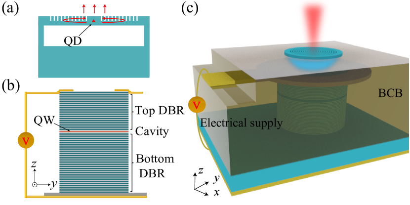
Figure 1 presents the building blocks and the concept of our device. A suspended GaAs CBG with a single QD embedded in the center serves as an efficient SPS , as shown in Fig. 1(a). The CBG consists of a GaAs microdisk surrounded by a serial of shallowly etched air trenches. Photons emitted from the QD in the center of CBG are mostly confined in the suspended membrane. Due to the presence of second-order Bragg gratings, parts of the emitted photons from the QD are scattered upwards for efficient collections and the others are reflected back to form a cavity for enhancing the strength of light-matter interactions davanco2011circular ; sapienza2015nanoscale ; wang2019demand ; abudayyeh2021single ; abudayyeh2021overcoming ; nikolay2018accurate . To optically pump the QD-CBG SPS, we explore electrically-injected micropillar lasers gies2019quantum consisting of quantum wells sandwiched between two distributed Bragg Reflectors (DBRs) [Fig. 1(b)]. These two elements are assembled in a way that the CBG is located right on top of the micropillar laser and an additional spacer is designed specifically to separate cavity modes in each distinct device, as schematically shown in Fig. 1(c). Optically driven by the coherent photons emitted from the electrically-injected micropillar laser, the QD in the CBG emits highly-directional single photons upwards to the collection optics.
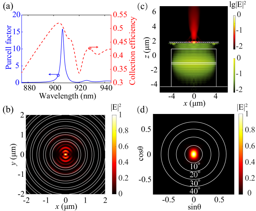
With the above device design, we further explore the optical performance of a single-QD in the hybrid cavities by modeling the extraction efficiency and the Purcell factor, as shown in Fig. 2(a). The extraction efficiency is defined as the fraction of the photons collected by the objective over all the photons emitted by the QD. The cavity effect of the CBG is revealed by a Lorentzian shape of the Purcell factor with a maximal value of 15 and a full width at half maximum of 3 nm, corresponding to a Q-factor of 303. The bandwidth for efficient collections of the single photons are much broader, showing extraction efficiencies >40% over 33 nm. Such an appreciable Purcell factor is due to the tight light confinement of the CBG cavity mode, as presented in Fig. 2(b). We chose a 2 m gap filled with benzocyclobutene (BCB) between the CBG and the micropillar laser so that the cavity mode of the CBG is not perturbed by the presence of the micropillar. The excitation of the QD by the micropillar laser (blue) and the highly-directional single-photon emissions (red) can be clearly identified from the beam propagation profiles in the XZ plane of the device, as shown in the Fig. 2(c). Fig. 2(d) further shows the far-field pattern of single-photon emissions from the CBG device, exhibiting a divergent angle within 10 degree for the efficient collection.
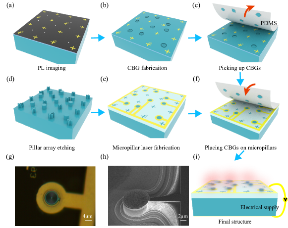
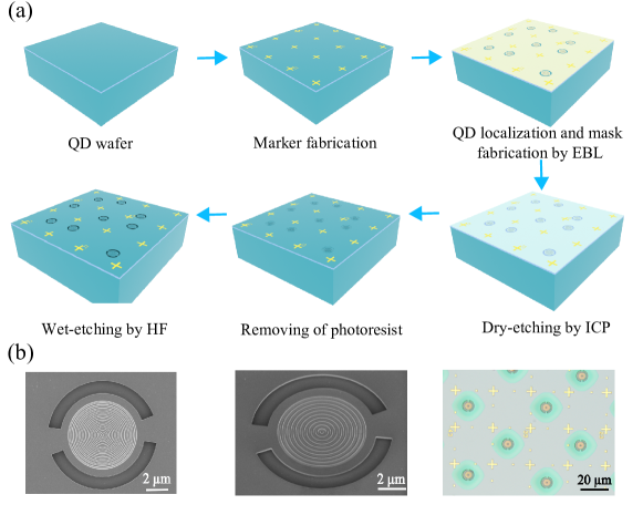
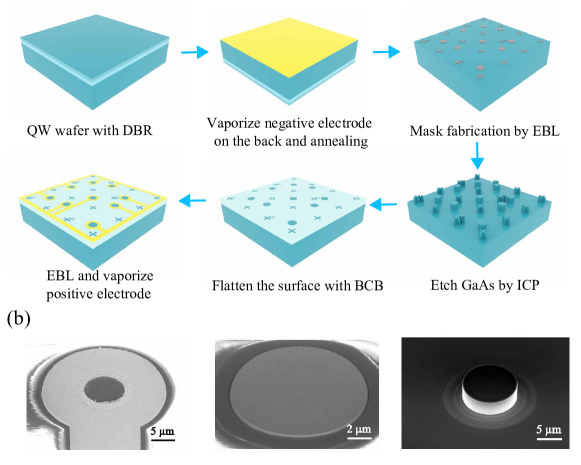
We take advantage of the well-developed transfer printing technique which has been successfully demonstrated for building hybrid quantum photonic devices katsumi2018transfer ; katsumi2019quantum ; jin2022generation . However, the implementations of such a technique to QD devices so far are limited in a one-by-one fashion due to the intrinsic random nature in QD’s spatial position. In order to obtain multiple devices with high yields at one time, we utilized the wide-field PL imaging technique to deterministically fabricate coupled CBG-QD devices sapienza2015nanoscale ; liu2017cryogenic ; liu2021nanoscale . In such a process, metallic alignment marks were firstly prepared on an III-V QD wafer and then the spatial positions of individual QDs respective to the alignment marks were extracted from PL images [Fig. 1(a)]. The deterministically coupled QD SPSs were then obtained by an aligned E-beam lithography, a chloride-based dry etch and a selective wet etch, as presented in Fig. 3(b). Then, we used transfer printing to pick up multiple processed CBGs from the substrate using a transparent rubber stamp [Fig. 3(c)]. On the other III-V wafer containing quantum wells and DBRs, electrically-injected microlasers were fabricated in a specific array based on the relative positions of fabricated CBGs, with the similar processing recipe for micropillar SPSs liu2021dual ; wei2022tailoring , as shown in Fig. 3(d,e). The micropillar array was covered with a 2m thick BCB spacer between the microlaser and SPS in order to maintain the cavity modes of the on-substrate CBGs. Because the cavity mode slightly leak out of the thin membrane in z direction, as shown in Fig. S(5), direct placements of CBGs on tops of micropillars result in the vanish of CBG modes, significantly reducing the brightness of the SPSs. We then aligned multiple CBGs to the micropillar laser array under an optical microscope and released the CBGs on micropillars by slowly and gently peeling the stamp off [Fig 3(f)]. A schematic of the completed hybrid integrated SPS array is shown in Fig. 3(i), in which multiple QDs coupled to CBGs can be simultaneously pumped by the underneath electrically-injected micropillar laser array. In a representative microscope image of the transferred device [Fig. 3(g)], a CBG can be clearly identified in the center of the micropillar laser. The successful transfer printing with a high alignment accuracy was further supported by a scanning electron microscope (SEM) image of a test device without planarizing the micropillar laser using BCB, as presented in Fig. 3(h).
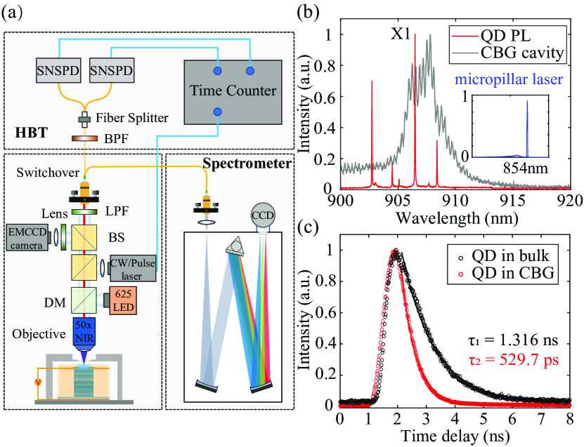
The optical setup and the device characterizations are shown in Fig. 4. The hybrid integrated devices are placed on three-dimensional nanopositioners located in a closed circle cryostat with a base temperature of 5.4 K. The QD SPSs can be either excited by the on-chip micropillar lasers or by external continuous wave (CW) and pulsed lasers via a 50 X objective with a numerical aperture of 0.65. The emitted single photons are collected by the same objective and sent to a monochromator for the spectral analysis or to single-photon detectors for lifetime characterizations and Hanbury-Brown-Twiss (HBT) measurements, as shown in Fig. 4(a). By applying a small bias voltage to the micropillar laser, single sharp excitonic lines (red) from the single QD are identified in the PL spectrum, as presented in Fig. 4(b). The bright exciton (X1) is spectrally close to the cavity mode (black) of the CBG. The emission spectrum of the electrically-injected micropillar laser is shown in the inset of Fig. 4(b), featuring a sharp lasing peak at 854 nm. Such near-infrared micropillar lasers are compatible with industry-standard, which renders practical application of our hybrid QDs SPS-Micropillar laser device convenient. The coupling between the QD and the CBG was revealed by the shortened lifetime of X1. A lifetime of 529 ps for QD in the CBG was extracted, corresponding to a Purcell factor of 2.5 compared to a lifetime of 1316 ps for the QD in bulk. The large deviation of the simulated Purcell factor from the experimental result is a combination of the non-ideal QD position and the long carrier relaxation time under above-band excitation liu2018high .
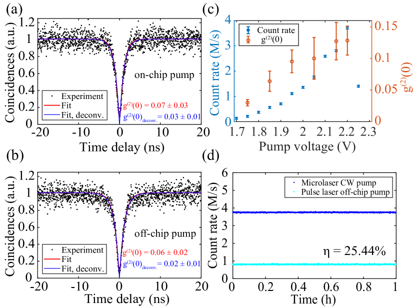
A single-photon purity g2(0) as low as 0.030.01 (deconvoluted with the detector response davanco2017heterogeneous ) under on-chip excitation condition was extracted from the second-order correlation measurement in an HBT interferometer, see Fig. 5(a). As a comparison, we used an external CW diode laser at 854 nm to excite the QD and obtained a very similar g2(0) of 0.020.01 [Fig. 5(b)], which suggests that the on-chip optical excitation by integrated lasers can deliver the same performance as that obtained under the widely-used external optical pumping. The photon count rate and g2(0) as a function of the bias voltage are shown in Fig. 5(c). Both photon flux and g2(0) increase madsen2014efficient ; kolatschek2021bright ; xu2022bright with the rise of the applied bias voltage and the maximal count rate (not saturated) up to 3.8 M/s with a g2(0) of 0.130.02 was obtained under the voltage of 2.2 V. Further increase of the bias voltage results in a rapid quenching of single-photon emissions, which is probably due to the detrimental thermal effect associated with the BCB spacer. We further quantified the extraction efficiency of the hybrid integrated SPS by externally exciting the device using a femto-second (fs) pulsed laser with a repetition rate of 79.6 MHz. The saturated count rate under pulsed excitation (see Fig. S10) together with the count rate under on-chip CW pumping are presented in Fig. 5(d). The generated photon rate is monitored continuously over 1 hour to check the long-term operational stability of the device. Under the pulsed excitation, each laser pulse is presumably to generate one single photon lodahl2015interfacing . By measuring the count rate in the single-photon detector and carefully calibrating the system detection efficiency (see details in SI), an extraction efficiency of 25.44% was obtained for the hybrid integrated SPSs.
III Discussion
To conclude, we have demonstrated hybrid integrations of bright SPSs with on-chip electrically-injected micropillar lasers. Assisted by the QD PL imaging technique, our optimized transfer printing process operates at a multi-device level, showing potential scalability for hybrid integrated quantum photonics. The single QD in the CBG was optically pumped by an on-chip micropillar laser, exhibiting a CW photon count rate of 3.8 M/s with g2(0) of 0.130.02 under a high bias voltage and a very low g2(0) of 0.030.01 under a low bias voltage. Our device experienced a Purcell factor of 2.5 and an extraction efficiency of 25.44% thanks to the coupling of QD to the CBG cavity mode. This work serves as a crucial step towards energy-saving on-chip single-photon and entangled pair sources for hybrid integrated quantum photonics. Our devices could be simultaneously coupled to an optical fiber array to realize the plug-and-play function, which has broad application prospects in quantum key distribution. Moving forwards, on-chip resonant excitations (see a realistic proposal in SI) by spectrally tuning the microlaser wavelength to the QD transition energies could be pursued to further improve the photon indistinguishability for advancing photonic quantum technologies.
IV Methods
Epitaxial growth of QDs:
The samples were grown using solid source molecular beam epitaxy on semi-insulating GaAs (001) substrates. After deoxidization at a temperature of 680 for 10 minutes and growth of 300 nm GaAs buffer layer at 660 , a 1000 nm sacrificial layer was grown at 620 . The InAs QDs were embedded in the middle of a GaAs layer with a thickness of 160 nm. The InAs QDs were deposited at the temperature of (Tc-27) with an indium flux rate of 0.004 ML/s and an As flux pressure of 5x Torr. The deposition temperatures are calibrated by the transition temperature Tc when the surface reconstruction pattern of GaAs in high-energy electron diffraction (RHEED) transfers from (2 × 4) to (2 × 3). Then the InAs QDs were capped with a thin layer of 0.3 nm AlAs and 6.5 nm GaAs, followed by a 200s indium flushing step at 660 X.
Fabrication of the coupled QD-CBG:
The process starts with the III-V wafer consists of a 160 nm-thin GaAs membrane containing InAs quantum dots (QDs) grown on top of a sacrificial layer (1 m ) and a GaAs substrate. To acquire the positions of QDs, firstly, metallic alignment marks are created on the surface of the sample with standard E-beam lithography, metal deposition and lift-off processes. Then, the positions of the QDs respective to the alignment marks are extracted from the wide-field PL images. The PL imaging process has an accuracy of about 20 nm he2017deterministic . After that, the shallow etched CBGs with QD in the center are fabricated through another aligned E-beam lithography followed by a chlorine-based dry etch process. After removing the photoresist by oxygen plasma surface treatments, we dip the sample in the acid solution of HF 10% for the necessary time to remove the sacrificial layer. We finally obtain the suspended deterministically coupled QD-CBG devices by drying the sample in isopropanol. The detailed fabrication flow of the coupled QD-CBG devices is presented at Supplementary Fig. S1.
Fabrication of the micropillar laser:
The wafer consists of a single layer GaAs with QW between 23(30) top(bottom) GaAs/ distributed Bragg reflector (DBRs) provided by EPIHOUSE. In order to achieve an electrically pumped micropillar laser, we need to properly dop the wafers. The epitaxial n-type and p-type regions are realized by doping the GaAs during the growth with silicon and carbon, respectively. The first step in creating the micropillar laser is the fabrication of electrical contacts to the n-doped layers. We obtain the Ni/Ge/Au/Ni/Au contacts on the back of the wafer by E-beam evaporation, followed by an annealing process. Then, the masks of the electrically-injected micropillar lasers and alignment marks are fabricated in a specific array based on the relative positions of fabricated CBGs by using an E-beam lithography. After the chlorine-based dry etch process, we use BCB to flatten the micropillars to ensure that the upper surfaces of the micropillars are just exposed. This process requires multiple spin-coatings of the photoresist, annealing and dry etching processes. Finally, the positive electrode is created by using an E-beam lithography, metal evaporation and lift-off processes. The detailed fabrication flow of the micropillar laser is presented at Supplementary Fig. S2.
Transfer printing process:
After the fabrications of the CBGs, we realize the micropillars at the corresponding positions according to the layout of the CBG array. Therefore, during the transfer process, we can align multiple CBGs with micropillars to achieve potentially scalable device integrations.We show three of 8 transferred devices at one time in Supplementary Fig. S3.
Acknowledgements: This research was supported by National Key Research and Development Program of China (2018YFA0306103); National Natural Science Foundation of China (11874437, 62035017); Hisilicon Technologies CO., LIMITED and the national super-computer center in Guangzhou.
Conflit of interest: The authors declare no conflict of interest.
Author contributions: Y. L. C and J. L conceived the project. X. S. L, R. B. S and S. F. L performed numerical simulations. C. K. S, Y. Y, H. Q. N, H. Q. L, X. B. S and Z. C. N grew the wafers. X. S. L, J. T. M and S. F. L performed optical characterizations. X. S. L, W. G, S. F. L and J. L analyzed the data. J. L wrote the manuscript with inputs from all authors. Z. C. N, Y. L. C and J. L supervised the project.
References
- (1) O’brien, J. L., Furusawa, A. & Vučković, J. Photonic quantum technologies. Nature Photonics 3, 687–695 (2009).
- (2) Wang, J., Sciarrino, F., Laing, A. & Thompson, M. G. Integrated photonic quantum technologies. Nature Photonics 14, 273–284 (2020).
- (3) Elshaari, A. W., Pernice, W., Srinivasan, K., Benson, O. & Zwiller, V. Hybrid integrated quantum photonic circuits. Nature Photonics 14, 285–298 (2020).
- (4) Kim, J.-H., Aghaeimeibodi, S., Carolan, J., Englund, D. & Waks, E. Hybrid integration methods for on-chip quantum photonics. Optica 7, 291–308 (2020).
- (5) Senellart, P., Solomon, G. & White, A. High-performance semiconductor quantum-dot single-photon sources. Nature Nanotechnology 12, 1026–1039 (2017).
- (6) Wang, H. et al. Towards optimal single-photon sources from polarized microcavities. Nature Photonics 13, 770–775 (2019).
- (7) Tomm, N. et al. A bright and fast source of coherent single photons. Nature Nanotechnology 16, 399–403 (2021).
- (8) He, Y.-M. et al. Deterministic implementation of a bright, on-demand single-photon source with near-unity indistinguishability via quantum dot imaging. Optica 4, 802–808 (2017).
- (9) Uppu, R. et al. Scalable integrated single-photon source. Science Advances 6, eabc8268 (2020).
- (10) Qiang, X. et al. Large-scale silicon quantum photonics implementing arbitrary two-qubit processing. Nature Photonics 12, 534–539 (2018).
- (11) Li, L. et al. Metalens-array–based high-dimensional and multiphoton quantum source. Science 368, 1487–1490 (2020).
- (12) Wang, J. et al. Multidimensional quantum entanglement with large-scale integrated optics. Science 360, 285–291 (2018).
- (13) Zhang, M. et al. Generation of multiphoton quantum states on silicon. Light: Science & Applications 8, 1–7 (2019).
- (14) Davanco, M. et al. Heterogeneous integration for on-chip quantum photonic circuits with single quantum dot devices. Nature Communications 8, 1–12 (2017).
- (15) Zadeh, I. E. et al. Deterministic integration of single photon sources in silicon based photonic circuits. Nano Letters 16, 2289–2294 (2016).
- (16) Katsumi, R. et al. Quantum-dot single-photon source on a cmos silicon photonic chip integrated using transfer printing. APL Photonics 4, 036105 (2019).
- (17) Katsumi, R., Ota, Y., Kakuda, M., Iwamoto, S. & Arakawa, Y. Transfer-printed single-photon sources coupled to wire waveguides. Optica 5, 691–694 (2018).
- (18) Schwartz, M. et al. Fully on-chip single-photon hanbury-brown and twiss experiment on a monolithic semiconductor–superconductor platform. Nano Letters 18, 6892–6897 (2018).
- (19) Najafi, F. et al. On-chip detection of non-classical light by scalable integration of single-photon detectors. Nature Communications 6, 1–8 (2015).
- (20) Reithmaier, G. et al. On-chip time resolved detection of quantum dot emission using integrated superconducting single photon detectors. Scientific Reports 3, 1–6 (2013).
- (21) He, Y.-M. et al. On-demand semiconductor single-photon source with near-unity indistinguishability. Nature Nanotechnology 8, 213–217 (2013).
- (22) Gschrey, M. et al. Highly indistinguishable photons from deterministic quantum-dot microlenses utilizing three-dimensional in situ electron-beam lithography. Nature Communications 6, 1–8 (2015).
- (23) Wei, Y. et al. Tailoring solid-state single-photon sources with stimulated emissions. Nature Nanotechnology 17, 470–476 (2022).
- (24) Jayakumar, H. et al. Deterministic photon pairs and coherent optical control of a single quantum dot. Physical Review Letters 110, 135505 (2013).
- (25) Reindl, M. et al. Phonon-assisted two-photon interference from remote quantum emitters. Nano Letters 17, 4090–4095 (2017).
- (26) Thomas, S. et al. Bright polarized single-photon source based on a linear dipole. Physical Review Letters 126, 233601 (2021).
- (27) Schlehahn, A. et al. An electrically driven cavity-enhanced source of indistinguishable photons with 61% overall efficiency. APL Photonics 1, 011301 (2016).
- (28) Kreinberg, S. et al. Quantum-optical spectroscopy of a two-level system using an electrically driven micropillar laser as a resonant excitation source. Light: Science & Applications 7, 1–9 (2018).
- (29) Munnelly, P. et al. Electrically tunable single-photon source triggered by a monolithically integrated quantum dot microlaser. Acs Photonics 4, 790–794 (2017).
- (30) Stock, E. et al. On-chip quantum optics with quantum dot microcavities. Advanced Materials 25, 707–710 (2013).
- (31) Lee, J. et al. Electrically driven and electrically tunable quantum light sources. Applied Physics Letters 110, 071102 (2017).
- (32) Davanco, M., Rakher, M. T., Schuh, D., Badolato, A. & Srinivasan, K. A circular dielectric grating for vertical extraction of single quantum dot emission. Applied Physics Letters 99, 041102 (2011).
- (33) Sapienza, L., Davanço, M., Badolato, A. & Srinivasan, K. Nanoscale optical positioning of single quantum dots for bright and pure single-photon emission. Nature Communications 6, 1–8 (2015).
- (34) Wang, H. et al. On-demand semiconductor source of entangled photons which simultaneously has high fidelity, efficiency, and indistinguishability. Physical Review Letters 122, 113602 (2019).
- (35) Abudayyeh, H. et al. Single photon sources with near unity collection efficiencies by deterministic placement of quantum dots in nanoantennas. APL Photonics 6, 036109 (2021).
- (36) Abudayyeh, H. et al. Overcoming the rate-directionality trade-off: A room-temperature ultrabright quantum light source. ACS Nano 15, 17384–17391 (2021).
- (37) Nikolay, N. et al. Accurate placement of single nanoparticles on opaque conductive structures. Applied Physics Letters 113, 113107 (2018).
- (38) Gies, C. & Reitzenstein, S. Quantum dot micropillar lasers. Semiconductor Science and Technology 34, 073001 (2019).
- (39) Jin, T. et al. Generation of polarization-entangled photons from self-assembled quantum dots in a hybrid quantum photonic chip. Nano Letters 22, 586–593 (2022).
- (40) Liu, J. et al. Cryogenic photoluminescence imaging system for nanoscale positioning of single quantum emitters. Review of Scientific Instruments 88, 023116 (2017).
- (41) Liu, S., Srinivasan, K. & Liu, J. Nanoscale positioning approaches for integrating single solid-state quantum emitters with photonic nanostructures. Laser & Photonics Reviews 15, 2100223 (2021).
- (42) Liu, S. et al. Dual-resonance enhanced quantum light-matter interactions in deterministically coupled quantum-dot-micropillars. Light: Science & Applications 10, 1–7 (2021).
- (43) Liu, F. et al. High purcell factor generation of indistinguishable on-chip single photons. Nature Nanotechnology 13, 835–840 (2018).
- (44) Madsen, K. H. et al. Efficient out-coupling of high-purity single photons from a coherent quantum dot in a photonic-crystal cavity. Physical Review B 90, 155303 (2014).
- (45) Kolatschek, S. et al. Bright purcell enhanced single-photon source in the telecom o-band based on a quantum dot in a circular bragg grating. Nano Letters 21, 7740–7745 (2021).
- (46) Xu, S.-W. et al. Bright single-photon sources in the telecom band by deterministically coupling single quantum dots to a hybrid circular bragg resonator. Photonics Research 10, B1–B6 (2022).
- (47) Lodahl, P., Mahmoodian, S. & Stobbe, S. Interfacing single photons and single quantum dots with photonic nanostructures. Reviews of Modern Physics 87, 347 (2015).
SUPPLEMENTARY INFORMATION
I Characterization of the QD wafer
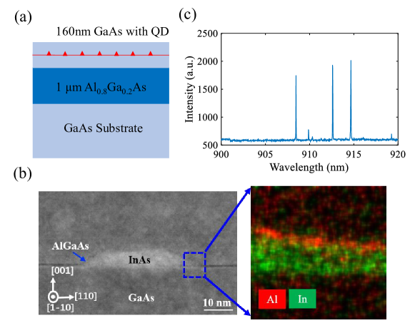
The QD wafer is schematically shown in Fig. S1(a), consisting of a 160 nm-thin GaAs membrane containing InAs quantum dots (QDs), a sacrificial layer (1 m ) and a GaAs substrate. Fig. S1(b) shows the high-resolution high-angle annular dark field (HAADF) STEM images along [110] crystallographic direction of single InAs QD. The bright regions close to the center of the image represent the InAs QDs, with the average height of 6 nm. The AlGaAs capping layer can be clearly presented as the darker region surrounding the QD. A representative spectrum of single QD is shown in Fig. S1(c).
II Fabrication flow of the CBG
The full fabrication flow of deterministically coupled QD-CBG is shown in Fig. S2(a). The process starts with the III-V wafer consists of a 160 nm-thin GaAs membrane containing InAs quantum dots (QDs) grown on top of a sacrificial layer (1m ) and a GaAs substrate. To acquire the positions of QDs, firstly, metallic alignment marks are created on the surface of the sample with standard E-beam lithography, metal deposition and lift-off processes. Then, the positions of the QDs respective to the alignment marks are extracted from the wide-field PL images. After that, the shallow etched CBGs with QD in the center are fabricated through another aligned E-beam lithography followed by a chlorine-based dry etch process. After removing the photoresist by oxygen plasma surface treatments, we dip the sample in the acid solution of HF 10% for the necessary time to remove the sacrificial layer. We finally obtain the suspended deterministically coupled QD-CBG devices by drying the sample in isopropanol, as shown in Fig. S2(b). The parameters of CBG during fabrication are carefully chosen to ensure the spectral matching between the X state of the QD and the fundamental cavity mode of the CBG.
III Fabrication flow of the micropillar laser
The full fabrication flow of the micropillar laser is shown in Fig. 3(a). The wafer consists of a single layer GaAs with QW between 23(30) top(bottom) GaAs/ distributed Bragg reflector (DBRs) provided by EPIHOUSE. In order to achieve an electrically pumped micropillar laser, we need to properly dop the wafers. The epitaxial n-type and p-type regions are realized by doping the GaAs during the growth with silicon and carbon, respectively. The first step in creating the micropillar laser is the fabrication of electrical contacts to the n-doped layers. We obtain the Ni/Ge/Au/Ni/Au contacts on the back of the wafer by E-beam evaporation, followed by an annealing process. Then, the masks of the electrically-injected micropillar lasers and alignment marks are fabricated in a specific array based on the relative positions of fabricated CBGs by using an E-beam lithography. After the chlorine-based dry etch process, we use BCB to flatten the micropillars to ensure that the upper surfaces of the micropillars are just exposed. This process requires multiple spin-coatings of the photoresist, annealing and dry etching processes. Finally, the positive electrode is created by using an E-beam lithography, metal evaporation and lift-off processes. The SEM images of the samples are shown in Fig. S3(b).
IV Transfer printing process for multiple devices
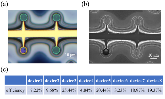
After the fabrications of the CBGs, we realize the micropillars at the corresponding positions according to the layout of the CBG array. Therefore, during the transfer process, we can align multiple CBGs with micropillars to achieve potentially scalable device integrations. We show three of 8 transferred devices at one time in Fig. S4(a,b). The extraction efficiencies of each device are listed in Fig. S4(c), featuring high yields for the multiple device transfer printing process.
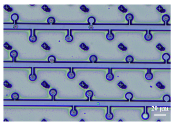
We further present the transferring of a large array of devices in Fig. S5. 20 out of 26 devices are successfully fabricated in a single run. The fabrication throughput and yield could be further boosted by exploiting commercially available tools that are specially designed for the transfer printing process.
V Numerical simulations of CBG
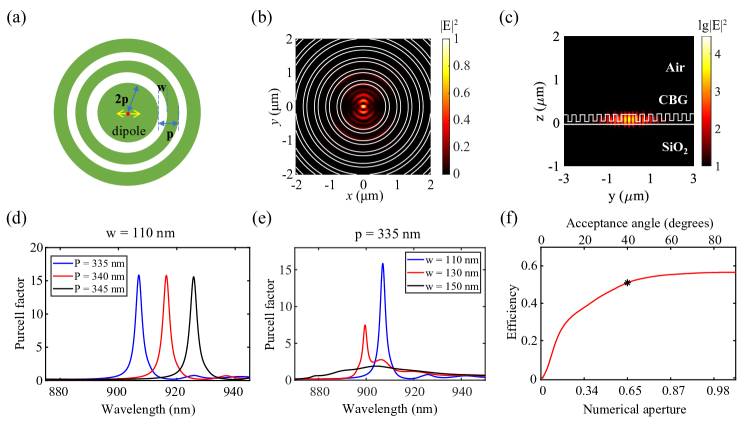
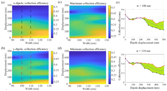
The design of CBG for QD single-photon sources has been thoroughly discussed in the literature davanco2011circular ; sapienza2015nanoscale . Here we briefly show the optimization of the parameters in Fig. S(6). We use the central disk with a radius of 2p in which p and w are the periodicity and the width of the etched trenches respectively, as shown in Fig. S6(a). The cavity modes in XY plane and YZ plane are plotted in Fig. S6(b,c) respectively. In Fig. S6(d), the cavity resonances for different p are shown. To match the QD emission wavelength ( 907 nm), we chose p=335 nm. We further change w in Fig. S6(e), and w=110 nm gives rise to the highest Purcell factor at the targeted wavelength. Finally, the extraction efficiency for the optimized parameter (p=335 nm and w=110 nm) as a function of NA is presented in Fig. S6(f).
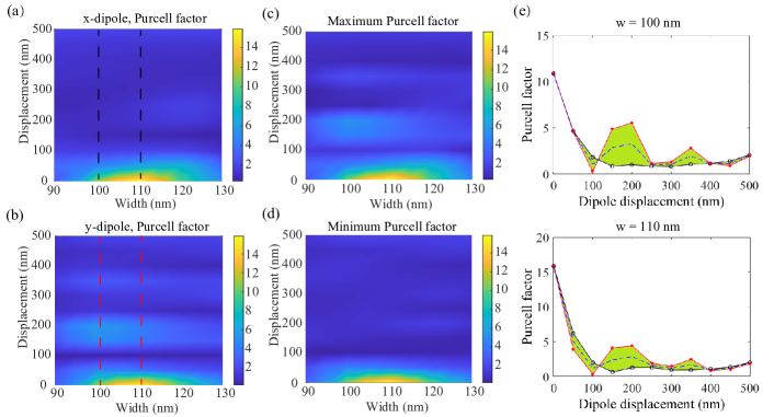
We further present the Purcell factor and extraction efficiency (with NA=0.65) as a function of the placement deviation and fabrication resolution in Fig. S7 and Fig. S8, respectively. The displacement refers the distance from QD to the center of the CBG. The fabrication resolution mostly reflects on the width of the etched trenches. Due to the uncertainty of the dipole orientation, we have simulated both x-polarized and y-polarized dipoles. The Purcell factors and extraction efficiencies of other orientated dipoles fall into the range between the x-polarized and y-polarized dipoles. sapienza2015nanoscale Compared to the simulations, our QD seems to be within 300 nm from the center of the CBG, which is probably due to an unintentional offset in the aligned electron beam lithography process.
VI Characterizations of microlasers
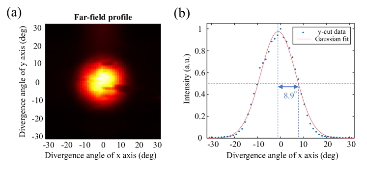
We’ve presented the far-field pattern of the microlaser in Fig. S9. The far-field emission is close to an Gaussian profile with a divergence angle below 10 degree.
VII Estimation of extraction efficiency
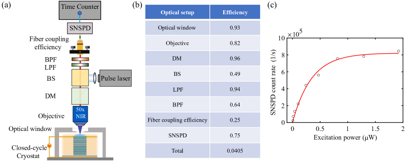
The extraction efficiency of the hybrid SPS at the first lens is evaluated by externally exciting the device using a femto-second pulsed laser with a repetition rate of 79.6 MHz. Fig. S10(a) shows the schematic of the experimental setup for estimating the extraction efficiency. The emitted photons are collected using a microscope objective with an NA of 0.65. For this measurement, the signals pass through a dichroscope (DM), a beam splitter (BS), a long pass filter (LPF), and a bandpass filter(BPF) before coupling into a single-mode fiber. The detection efficiency of the whole setup has been carefully calibrated to be 0.0405, as shown in Fig. S10(b). A saturation count rate of 0.82 MHz was extracted from Fig. S10(c), which results in an extraction efficiency at the first lens of 25.44%.
VIII Scheme for on-chip resonant excitation
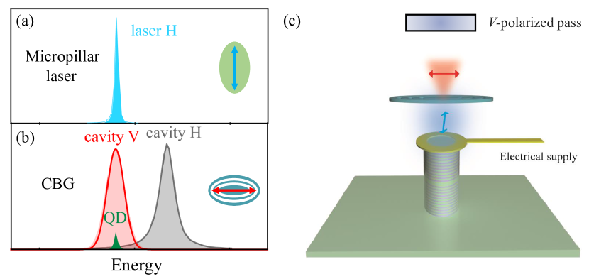
Inspired by recent works of exploiting asymmetrical microcavities for resonance fluorescence wang2019towards ; gerhardt2019polarization , we propose to employ an elliptical micropillar for obtaining a single-mode laser with H-polarization, as shown in Fig. S11(a). Meanwhile an asymmetrical CBG is employed in which a charged exciton is resonant with V-polarized cavity mode and the tail of H-polarized cavity mode is used for the resonant excitation, as shown in Fig. S11(b). In such a configuration, an external polarizer along V direction as shown in Fig. S11(c) will remove the H-polarized laser background and result in V-polarized single photons with a high indistinguishability.
IX Comparison to devices in the literature
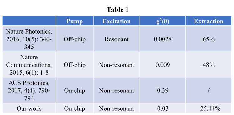
We’ve compared our devices with representative of the state-of-the-art in Table 1. Compared to the state-of-the-art devices under on-chip excitation, our device shows a much better single-photon purity and a higher extraction efficiency. However, the best reported devices under off-chip excitation still exhibit better metrics in terms of extraction efficiency, single-photon purity as well as the indistinguishability. We believe that the performance of our device could be further significantly improved with optimizations of the fabrication process and implementations of on-chip resonant excitation in Fig. S11.
References
- (1) Davanco, M., Rakher, M. T., Schuh, D., Badolato, A. & Srinivasan, K. A circular dielectric grating for vertical extraction of single quantum dot emission. Applied Physics Letters 99, 041102 (2011).
- (2) Sapienza, L., Davanço, M., Badolato, A. & Srinivasan, K. Nanoscale optical positioning of single quantum dots for bright and pure single-photon emission. Nature Communications 6, 1–8 (2015).
- (3) Wang, H. et al. Towards optimal single-photon sources from polarized microcavities. Nature Photonics 13, 770–775 (2019).
- (4) Gerhardt, S. et al. Polarization-dependent light-matter coupling and highly indistinguishable resonant fluorescence photons from quantum dot-micropillar cavities with elliptical cross section. Physical Review B 100, 115305 (2019).