Transition to an excitonic insulator from a two-dimensional conventional insulator
Abstract
In this work, first, we present a general formulation to investigate the ground-state and elementary excitations of an excitonic insulator (EI) in real materials. In addition, we discuss the out-of-equilibrium state induced (albeit transiently) by high-intensity light illumination of a conventional two-dimensional (2D) insulator. We then, present various band-structure models which allow us to study the transition from a conventional insulator to an EI in 2D materials as a function of the dielectric constant, the conventional insulator gap (and chemical potential), the bandwidths of the conduction and valence bands and the Bravais lattice unit-cell size. One of the goals of this investigation is to determine which range of these experimentally determined parameters to consider in order to find the best candidate materials to realize the excitonic insulator. The numerical solution to the EI gap equation for various band-structures shows a significant and interesting momentum-dependence of the EI gap function and of the zero-temperature electron and hole momentum-distribution across the Brillouin zone. Last, we discuss the fact that these features can be detected by tunneling microscopy.
I Introduction
The instability of the conventional insulating state to that of the so-called excitonic-insulator (EI) in semiconductors was pointed out and studied a long-time agoMott (1961); Knox (1963); Jérome et al. (1967); Halperin and Rice (1968); Kohn and Sherrington (1970). Within the Bose-Einstein condensation (BEC) framework, the EI state can occur when the electron–hole binding energy exceeds the charge bandgap; when this happens, clearly the conventional-insulator ground-state becomes unstable. The ground-state exciton population is then determined by balancing the negative exciton formation energy against the pair-exciton repulsion energy. It has been argued that in bulk materials the EI state can occur in small-bandgap semiconductors and small bandwidth semimetalsHalperin and Rice (1968). This phenomenon has also been investigated in connection with various aspects of the quantum many-boson problemZhu et al. (1995); Sun and Millis (2021); Eisenstein and MacDonald (2004); Kogar et al. (2017); Butov (2004); Baranov et al. (2012); the presence of repulsion among exciton pairs can stabilize superfluid and crystalline phases by means of suppression of density and phase fluctuationsBaranov et al. (2012); Lozovik et al. (2007); Ha et al. (2013). Spectroscopic evidence for EIs in various materials has been reportedKogar et al. (2017); Cercellier et al. (2007); Seki et al. (2014); Du et al. (2017); Ataei et al. (2021), however, conclusive evidence for the existence of such a state of matter remains elusive. In recent experimental work in transition metal dichalcogenide (TMD) double layers, it was arguedMa et al. (2021) that a quasi-equilibrium of spatially indirect exciton fluid can be established when the bias voltage applied between the two electrically isolated TMD layers was tuned to a range that populates bound electron–hole pairs, but not free electrons or holesXie and MacDonald (2018); Zeng and MacDonald (2020); Burg et al. (2018).
While the EI was originally conceived more than half a century ago, during the last decade several different families of two-dimensional (2D) or quasi-2D insulating or semiconducting materials have been synthesized; it might be reasonable to expect that once the relevant parameters of a properly chosen material are fine-tuned, such a material can become the host of this unique state of matter. The reason for holding this expectation for these pure 2D or quasi-2D materials is two fold. First, there are already reportsKogar et al. (2017); Cercellier et al. (2007); Seki et al. (2014); Du et al. (2017); Ataei et al. (2021); Wang et al. (2019) that show spectroscopic evidence for the existence of the EI state. Second, one expects a smaller average dielectric constant in single and double atomic layers due to the presence of vacuum or of a physical gap surrounding these layers. Examples of such materials are, carbon-based and related exfoliated 2D materials, the TMD mentioned above and organic–inorganic hybrid perovskitesStoumpos et al. (2016); Dou et al. (2015) where quantum wells can be engineered with chemical growth techniquesGao et al. (2019). The latter 2D perovskite structures can be understood as atomically thin slabs that are cut from the three-dimensional parent structures along different crystallographic directions, which are sandwiched by two layers of large organic cationsSaparov and Mitzi (2016).
In the present work, we describe a general formulation based on the linearization of the electron-hole interaction and by subsequent diagonalization of the resulting Bogoliubov-de Gennes Hamiltonian matrix. Then, we derive an analytic expression for a BCS-like gap-equation of the EI state. We iteratively solve the resulting gap equation to determine the full momentum dependence of the gap function, the EI ground-state electron and hole momentum distribution and the quasiparticle excitations of the excitonic state. We use a variety of interesting band-structure cases of two-dimensional materials and provide full numerical solution. Last, we study the transition to the EI state from the conventional-insulator state as a function of the parameters, dielectric constant, band-structure details including the bandwidth, the effective conventional-insulator gap and the Bravais lattice unit-cell size. This study is instructive for the search for the appropriate 2D materials which might be best suited to host this unconventional insulating state. In addition, we find some band-structures which host a more exotic EI state with regard to the bare-electron momentum distribution in the EI ground-state. This distribution displays peaks at non-trivial points inside the Brillouin zone that can play the role of a smoking gun for confirming the presence of the EI state by means of tunneling experimentsO’Mahony et al. (2022); Matt et al. (2020); Burg et al. (2018).
The paper is organized as follows. In Sec. II we present the formulation of the problem and its analytical aspects and we derive the gap equation for the most general case. In Sec. III we discuss the general features of the problem and how to find the best approach to search for materials which host the EI state. In Sec. IV we provide numerical solutions to the gap equation by iteratively solving the EI gap equation. In Sec. V we study the transition from the conventional-insulator to the EI state as a function of the band-structure parameters, the dielectric constant, etc. Last, in Sec. VI we give a summary of our results and conclusions and we discuss how to experimentally detect the EI state with its various features.
II Formulation
Let us start from the interaction term between electrons excited in the conduction band and those in the valence band in the simpler case where the interaction does not cause interband transitions, i.e.,
| (1) | |||
| (2) |
where is the Bloch state normalized in the volume of the crystal and is the Coulomb interaction screened by the dielectric matrix. Let us also define the hole creation and annihilation operators as
| (3) |
in terms of which and after changing dummy summation momentum label, the interaction term above takes the following form:
| (4) |
This form can be obtained from Eq. 2 by replacing the creation/annihilation operator of valence electrons by the hole creation/annihilation operator. Notice that the electron-hole interaction has the opposite sign, which means that there is an attractive interaction between electrons of the conduction band and holes in the valence band. This attractive interaction leads to formation of bound-states of electron-hole pairs which behave as bosons and which can form a BEC. In the weak coupling limit, this phenomenon can be approached as a BCS pairing state. To see how the latter can be described, we use the Bogoliubov-Valatin factorization approach for the interaction quartic term as follows:
| (5) | |||||
Using momentum conservation (i.e., ignoring Umklapp processes) we obtain:
| (6) | |||||
| (7) | |||||
| (8) |
The treatment of the resulting Hamiltonian
| (9) | |||||
where (and is standard. Notice that we have allowed for a different chemical potential between the valence () and conduction () bands. This difference may take into account the case where there is photoexcitation of the sample by means of laser-light illumination. The chemical potential difference controls the coexistence of electrons in the conduction band and holes in the valence band. This will occur for a transient time. In the case where the self-consistently determined value of is non-zero, there would be pairing of the electron-hole system.
Using the Bogoliubov-de Gennes matrix
| (10) |
the above Hamiltonian can be cast in the following form
| (11) | |||
| (12) | |||
| (13) | |||
| (14) |
The process of diagonalization of this Hamiltonian is described in the Appendix A. After carrying out the diagonalization, takes the diagonal form
| (15) |
where
| (16) | |||||
| (17) | |||||
| (18) |
and
| (19) | |||||
| (20) | |||||
| (21) | |||||
| (22) |
where corresponds to the eigenvalue and when , the operator . The operator corresponds to the eigenvalue and when , . The other two solutions which corresponds to the and eigenvalues are and operators which are the adjoint operators.
Now the interacting ground-state is defined as follows:
| (23) |
In order to calculate given by Eq. 8 above as an expectation value of
| (24) |
with respect to the interacting ground-state, we invert Eqs. 66,20 (see Appendix A). Using Eqs. 23 it is straightforward to show that
| (25) |
Therefore, the gap equation takes the form:
| (26) |
where is defined by Eq. 17. Notice that we have assumed that the effective interaction depends only on the momentum transfer. This equation needs to be solved iteratively to determine the gap function from the functions , , , which are assumed to be given.
As we will show, it is interesting to calculate the ground-state electron momentum distribution in the EI state. The electron momentum distribution, i.e., the ground-state expectation value of the bare electron and hole number operator is given as
| (27) |
These are the coherence factors that can be accessed by tunneling experiments and this is described in Sec. VI.


III General features and remarks
The approach discussed in the previous section is quite general and can be directly applied to real materials, using ab initio calculations. A band-structure calculation is required to determine the valence and conduction band energies and and their corresponding Bloch wavefunctions and . The effective interaction can be approximated using the random-phase-approximation (RPA) where is the Fourier transform of the Coulomb interaction screened by the dielectric function. The dielectric function in the RPAEhrenreich and Cohen (1959); Fry (1969) is given as
| (28) | |||||
| (29) | |||||
where is the volume of the crystal and is the zero temperature Fermi-Dirac distribution and taking the limit of correctly will yield the real part (i.e., the principal part of the momentum space integral) and the imaginary parts of .
Notice that as the conventional-insulator gap becomes smaller and smaller, something that has been widely discussed as a proper direction to take in order to enter the excitonic insulator phase, the dielectric function increases and this weakens the attractive interaction between electron-hole pairs. This works against the desired effect of producing a excitonic binding-energy greater than . As we will see below the dependence of on close to the conventional to excitonic-insulator transition can be stronger than its dependence on . As we will show, this depends on how far from the critical values of each of these parameters the material is.
One can naively try to make the same argument for the bandwidth, i.e., as the bandwidths of the conduction and valence bands decrease, the denominator of Eq. 29 decreases and the dielectric function should increase. However, this is not a correct conclusion, because the matrix element in the numerator also decreases, because the overlap between Wannier functions would decrease as the bandwidth decreases.
In the present paper, we plan to restrict ourselves to a variety of specific models which we would like to solve and which addresses the following question, the answer of which should aid the experimental search for an excitonic insulator: What are the relevant experimentally accessible parameters and how does the excitonic-insulator transition depend on each one of them? The electron-electron interaction in the insulator will be approximated by the screened Coulomb interaction which involves only a dielectric constant , i.e., we ignore the momentum and frequency dependence of the dielectric function and we only consider both the static and the long-wavelength limit. Notice that is directly accessible to experiments and it is clear that the candidate material to host the EI state should be selected to have an as small as possible. For this reason, we will restrict our models to two-dimensional materials where, because of the fact that the material is surrounded by vacuum, there is a good chance for the material to have a small average value of . In addition, just because is accessible to experiments, it will be an input parameter to our models and its microscopic determination will not be done here. As we will see below, there are a few other parameters which are also relevant and accessible to experiment (and to electronic-structure calculations).
IV Solution of the gap equation for two-dimensional materials
Next, we consider the case of two-dimensional materials using the Rytova-KeldyshRytova (1967) potential for a slab:
| (30) |
where and are the area and the thickness of a slab, and is the dielectric constant. We really do not know what the value of should be in a realistic case of a system, and, in addition, we prefer not to have too many free parameters. We will use a large enough value of ( is the atomic unit of length, i.e., the Bohr radius) where the results become insensitive to values of greater than that.
In the next several subsections we will consider variations of a two-band model, i.e., a single valence and single conduction band. We will consider the cases of a direct and of an indirect effective gap in Sec. IV.1 and Sec. IV.3. We note that, while the real conventional-insulator gap is positive, the effective gap can be tuned to zero or to a negative value, when the chemical potential for electrons and holes is effectively set to different values by the laser illumination. Therefore, in Sec. IV.2, we will examine the case where the effective gap vanishes and the case in which becomes negative. Lastly, in Sec. IV.4, we will study the case where the conduction band has four minima at the finite momenta , while the valence band has maxima at these points.
IV.1 Direct band-gap
First, we will consider the case of a direct gap using a single valence and and a single conduction band parametrized by the following dispersion relations:
| (31) |
where is the effective insulating gap. For simplicity and for avoiding using too many parameters, we will only consider the case of and an square lattice of area with periodic boundary conditions. In Eq. 26, the two-dimensional sum is over two independent integers and , which define the 2D vector from its components and , and each take values, i.e., .
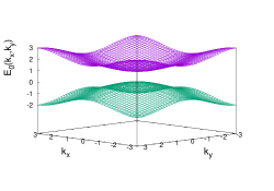
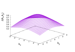
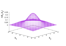
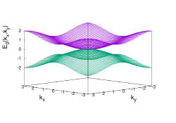
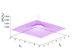
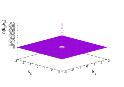
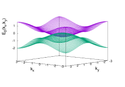
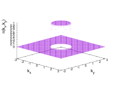
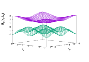
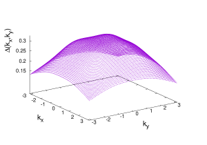
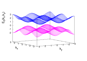
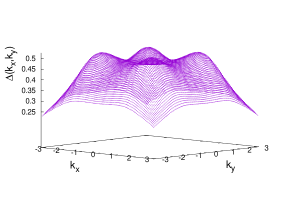
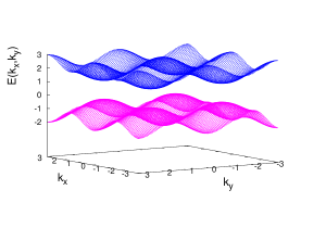
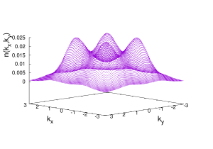
There is a range of the parameters, bandwidth , , and , where the gap equation, i.e., Eq. 26, has non-trivial solutions. This range and the transition to the excitonic insulator phase is investigated in Sec. V. In Fig. 1, the non-interacting band-structure is shown for the case of a effective gap eV and eV. For this case, the self-consistent solution to the gap equation, i.e., to Eq. 26, is shown in Fig. 1 using for dielectric constant and ( is the Bohr radius). Notice that the gap has significant momentum dependence and is larger at the point where the conduction (valence) band has its minimum (maximum). In Fig. 1 we present the two quasiparticle bands resulting for this case. Notice that they have a similar shape to the non-interacting conventional-insulator bands shown in Fig. 1. The most significant difference is in the vicinity of the point where the gap opens wider because the gap-function is larger near the point. In Fig. 1 we present the ground-state electron momentum distribution (i.e., given by Eq. 27). The hole momentum distribution is the same for this case because the valence and conduction bands are mirror symmetric with respect to the Fermi energy. Notice that its peak is at the point as expected.
IV.2 Zero and negative effective non-interacting gap
We used the band-structure given by Eq. 31 to investigate the case where the effective gap is zero or negative. In the case where the effective insulating gap of the non-interacting band-structure is zero and the chemical potentials for both bands are set to zero, we expect to find particle-hole pairing condensate for all values of the dielectric constant and of the rest of the other parameters. This is the well-known instability of the Fermi-liquid system when there is an attractive interaction present between fermionic species. As the value of becomes larger and larger the value of the gap will become smaller and smaller but never zero.
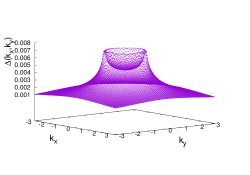
In Fig. 2, the non-interacting band-structure is shown for eV and . For this case, the self-consistent solution to the gap equation, i.e., to Eq. 26, is shown in Fig. 2 for and . In Fig. 2 the two quasiparticle bands are shown for the case of these parameters values. Notice that the gap which opens near the point is too small, i.e., with a maximum value eV, to be visible on the scale used in Fig. 2. In Fig. 2 we present the ground-state distribution of electrons in the conduction-band which has a sharp peak at the point.
In Fig. 3, the non-interacting band-structure is shown for the case of a negative effective gap eV and eV. For this case, the self-consistent solution to the gap equation, i.e., to Eq. 26, is shown in Fig. 3 for and . Notice the small-size of the EI gap and this is so because the dielectric constant is large. In addition, notice the singularities along the nodal line of the Fermi surface caused by the crossing of the two non-interacting bands. Fig. 3 illustrates the two quasiparticle bands for this case. In Fig. 3 we present the ground-state electron momentum distribution, which has a drumhead shape with its circular edge defined by the Fermi surface nodal line.
IV.3 Indirect band-gap
To investigate the presence of a non-trivial solution to the gap equation when the band-structure has an indirect gap, we consider the following simple band-structure:
| (32) |
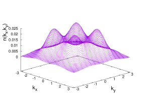
These bands, are shown in Fig. 4 using an effective gap eV and eV. Notice that the conduction band has a minimum at the point, while the valence band has a minimum at the point and four maxima at . Therefore, the indirect gap is from any of these four point of the valence band to the conduction-band energy at the point. For this case, the self-consistent solution to the gap equation is shown in Fig. 4 for and . Notice that is significantly reduced compared to the case of the direct gap. This is expected because in the indirect gap case the particle-hole density of states for a particle at and a hole at is significantly reduced in this case for the lowest energy excitations. The two quasiparticle bands are shown in Fig. 4 for this case. In Fig. 4 the ground-state momentum distribution of electrons in conduction-band is presented. Remarkably, there are four peaks at the valence-band maxima; the reason for this is that the energy-gap for a zero-momentum transfer excitation is minimum at the four points where the peaks are formed. Because the density of states of the conduction-band is finite at those same four points, the particle-hole density of states for a particle at and a hole at is reduced as compared to the direct-gap case. In the latter case, the density of states diverges at the point in both the conduction and valence bands.
IV.4 Multiple direct band-gaps
Here, we examine the case of a band-structure with multiple conduction-band minima which coincide with the valence-band maxima. Shown in Fig. 5 is an example of such a scenario, where the non-interacting band-structure is given by:
| (33) |
We have used an effective gap eV and eV. There are four such extrema of the conduction and valence band at . For this case, the self-consistent solution to the gap equation is shown in Fig. 5 for and where exhibits four maxima at those band extrema. In Fig. 5 the two quasiparticle bands are illustrated. Notice that, while the momentum dependence is similar to that of the non-interacting bands, the gap in the bands in the EI state is larger than that of the non-interacting conventional-insulator case. The ground-state momentum distribution of electrons occupying the conduction-band is presented in Fig. 5 and exhibits four rather well-defined peaks at the same momenta. The density of states of the conduction band diverge at the same four points as the valence band, therefore, the particle-hole density of states for a particle at and a hole at is very large at each one of those four points.
V Conventional to excitonic insulator transition
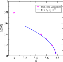
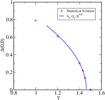
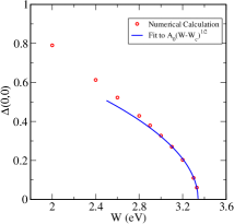
Here, we discuss the results of our investigation of the presence of a non-trivial solution to the gap equation, i.e., to Eq. 26, for the case of direct and positive effective gap using the simple dispersion given by the Eq. 31. We investigate the dependence of the EI gap on the parameters , and the bandwidth .
Figs. 6,6,6 illustrate the dependence of on each one of the parameters , and by fixing the values of other two. The solid blue lines represent fits to the formulae
| (34) | |||||
| (35) | |||||
| (36) |
near the critical values , and , as expected because of the mean-field character of the solution. The coefficients and the critical values are given in the caption of that figure. Notice that the agreement with the mean-field order-parameter critical exponent 1/2 is quite good near the critical point.
We note that for eV the required value of is less than 3.8. However, as the value of or decreases the value of becomes larger. For example, if we use eV and keep the rest of the parameters ( eV and ) the same, we obtain . We note that the value of the self-consistent solution for the gap does not depend independently on the parameters and . It depends on the product . So, the combination of the unit-cell size and has to be taken into consideration when searching for a good candidate material to realize the EI state.
VI Discussion and conclusions
We have studied the transition from the conventional-insulator state to that of an excitonic insulator in several cases of 2D band-structures with various different features. We find that the band-structures with a direct-gap (keeping all other band characteristics and the same) yield a larger EI gap as compared to the case of an indirect gap. The EI state in the case of an indirect gap or in the case of band-structures with direct gaps at wavevectors different than the -point, has a zero-temperature electron momentum distribution with peaks at such non-zero wavevectors.
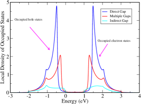
The electron momentum distribution is experimentally accessible by tunneling experiments. Tunneling experiments measure the local density of occupied states (LDOS) which, in our case, is given as
| (37) |
Therefore, can be calculated using the quasiparticle bands and the momentum distributions given by Eq. 27 and is illustrated in Fig. 7 for the cases of direct gap, indirect gap and multiple gaps discussed in Sec. IV.1, Sec. IV.3 and Sec. IV.4 respectively. In addition, if one is able to accurately measure the differential tunnel conductance as a function of location within the unit-cell of the Bravais lattice, then the electron/hole ground-state momentum distribution can be inferredO’Mahony et al. (2022); Matt et al. (2020).
Therefore, the zero-temperature electron momentum distribution, through the corresponding observable LDOS, can be used as a criterion for the presence of the EI state. In the case of insulators with an indirect gap or in materials with multiple direct-gap band-structures the momentum distribution develops peaks at non-zero -points in the Brillouin zone upon entering the EI state. These features can also be seen experimentally, if the LDOS is probed by measuring the differential tunnel conductance as a function of location and tip-sample voltageO’Mahony et al. (2022); Matt et al. (2020).
In the case of a direct-gap band-structure, we also studied the dependence of the non-trivial gap function solution, , on the various parameters, such as, the band-structure bandwidth and effective band-gap, as well its dependence on the dielectric constant of the 2D material. We find that the dependence of on parameters, such as, the dielectric constant , the bandwidth , and the effective band-gap near their corresponding critical values, is consistent with mean-field critical behavior as expected. More importantly, we find that conventional 2D insulators with not too-small gap (i.e., eV) and not too-small bandwidth (i.e., eV) can host an EI state, provided that the dielectric constant is smaller than approximately . Materials with larger values of must have smaller effective and/or .
Our results and conclusions should be relevant to real quasi-2D materials and superlattices. TMD monolayers or multilayers are structurally stable and display a variety of band gaps and dielectric properties. Those with smaller dielectric constant, smaller gap and narrow conduction and valence bands should be more promising to realize the excitonic insulator. Furthermore, the organic–inorganic hybrid perovskitesStoumpos et al. (2016); Dou et al. (2015); Gao et al. (2019) might be a suitable class of materials to search for a potential realization of the EI state. These insulators form a superlattice structure where the perovskite layers are separated from each other by means of organic molecules. One should select the organic molecules to be among those with relatively small dielectric constant and the atoms which form the halide-perovskite layer should be selected to yield a relatively small gap with as narrow as possible valence and conduction bands nearest to the Fermi level.
VII Acknowledgment
I would like to thank Hanwei Gao for useful interactions. This work was supported by the U.S. National Science Foundation under Grant No. NSF-EPM-2110814.
Appendix A Diagonalization of the Bogoliubov-de Gennes matrix
Next we diagonalize the matrix to find its eigenstates and its corresponding eigenvalues. We notice that the matrix has the following form:
| (38) |
where and are the following matrices:
| (39) |
and is the complex conjugate (not the adjoint) of the matrix . The diagonalization equation:
| (40) |
splits into the following two matrix equations:
| (41) |
Now, Eq. 41 yields
| (42) |
The inverse of the matrix is
| (43) |
Now, using Eq. 42 and by writing
| (44) |
we find that
| (45) |
Now, Eq. 41 yields
| (46) |
The inverse of the matrix is
| (47) |
which lead to the following relations:
| (48) |
Eqs 48,45 have to be simultaneously satisfied. This leads to the following equations:
| (49) | |||||
| (50) |
However, if both and are assumed to be non-zero, then, this leads to
| (51) |
i.e., to , which can only be satisfied by the trivial solution , because of the structure of the matrix .
However, we have the alternative solutions that either a) and or b) and .
a) , and using Eqs 48 we obtain
| (52) |
This equation determines the eigenvalues in this case to be given as
| (53) | |||||
| (54) | |||||
| (55) |
In this case the non-zero coefficients are related as follows
| (56) |
and after normalization (and choosing an overall phase factor) the corresponding eigenvectors are obtained as
| (57) | |||||
| (58) | |||||
| (59) |
b) . In this case using Eqs 45
| (60) |
The latter equation determines the eigenvalues in this case to be given as
| (61) |
After normalization (and choosing an overall phase factor) the corresponding eigenvectors are obtained as
| (62) | |||||
| (63) | |||||
| (64) |
In summary, after normalizing the coefficients, we obtain the following solutions
| (65) | |||||
| (66) | |||||
| (67) | |||||
| (68) |
where corresponds to the eigenvalue and when , the operator . The operator corresponds to the eigenvalue and when , . The other two solutions which correspond to the and eigenvalues are the and operators which are the adjoint operators.
References
- Mott (1961) N. F. Mott, The Philosophical Magazine: A Journal of Theoretical Experimental and Applied Physics 6, 287 (1961).
- Knox (1963) R. S. Knox, in Solid State Physics, edited by F. Seitz and D. Turnbull (Accademic Press Inc., New York, 1963) Chap. Suppl. 5, p. 100.
- Jérome et al. (1967) D. Jérome, T. M. Rice, and W. Kohn, Phys. Rev. 158, 462 (1967).
- Halperin and Rice (1968) B. I. Halperin and T. M. Rice, Rev. Mod. Phys. 40, 755 (1968).
- Kohn and Sherrington (1970) W. Kohn and D. Sherrington, Rev. Mod. Phys. 42, 1 (1970).
- Zhu et al. (1995) X. Zhu, P. B. Littlewood, M. S. Hybertsen, and T. M. Rice, Phys. Rev. Lett. 74, 1633 (1995).
- Sun and Millis (2021) Z. Sun and A. J. Millis, Phys. Rev. Lett. 126, 027601 (2021).
- Eisenstein and MacDonald (2004) J. P. Eisenstein and A. H. MacDonald, Nature 432, 691 (2004).
- Kogar et al. (2017) A. Kogar, M. S. Rak, S. Vig, A. A. Husain, F. Flicker, Y. I. Joe, L. Venema, G. J. MacDougall, T. C. Chiang, E. Fradkin, J. van Wezel, and P. Abbamonte, Science 358, 1314 (2017).
- Butov (2004) L. V. Butov, Journal of Physics: Condensed Matter 16, R1577 (2004).
- Baranov et al. (2012) M. A. Baranov, M. Dalmonte, G. Pupillo, and P. Zoller, Chemical Reviews 112, 5012 (2012).
- Lozovik et al. (2007) Y. E. Lozovik, I. Kurbakov, G. Astrakharchik, J. Boronat, and M. Willander, Solid State Communications 144, 399 (2007).
- Ha et al. (2013) L.-C. Ha, C.-L. Hung, X. Zhang, U. Eismann, S.-K. Tung, and C. Chin, Phys. Rev. Lett. 110, 145302 (2013).
- Cercellier et al. (2007) H. Cercellier, C. Monney, F. Clerc, C. Battaglia, L. Despont, M. G. Garnier, H. Beck, P. Aebi, L. Patthey, H. Berger, and L. Forró, Phys. Rev. Lett. 99, 146403 (2007).
- Seki et al. (2014) K. Seki, Y. Wakisaka, T. Kaneko, T. Toriyama, T. Konishi, T. Sudayama, N. L. Saini, M. Arita, H. Namatame, M. Taniguchi, N. Katayama, M. Nohara, H. Takagi, T. Mizokawa, and Y. Ohta, Phys. Rev. B 90, 155116 (2014).
- Du et al. (2017) L. Du, X. Li, W. Lou, G. Sullivan, K. Chang, J. Kono, and R.-R. Du, Nature Communications 8, 1971 (2017).
- Ataei et al. (2021) S. S. Ataei, D. Varsano, E. Molinari, and M. Rontani, Proceedings of the National Academy of Sciences 118, e2010110118 (2021).
- Ma et al. (2021) L. Ma, P. X. Nguyen, Z. Wang, Y. Zeng, K. Watanabe, T. Taniguchi, A. H. MacDonald, K. F. Mak, and J. Shan, Nature 598, 585 (2021).
- Xie and MacDonald (2018) M. Xie and A. H. MacDonald, Phys. Rev. Lett. 121, 067702 (2018).
- Zeng and MacDonald (2020) Y. Zeng and A. H. MacDonald, Phys. Rev. B 102, 085154 (2020).
- Burg et al. (2018) G. W. Burg, N. Prasad, K. Kim, T. Taniguchi, K. Watanabe, A. H. MacDonald, L. F. Register, and E. Tutuc, Phys. Rev. Lett. 120, 177702 (2018).
- Wang et al. (2019) Z. Wang, D. A. Rhodes, K. Watanabe, T. Taniguchi, J. C. Hone, J. Shan, and K. F. Mak, Nature 574, 76 (2019).
- Stoumpos et al. (2016) C. C. Stoumpos, D. H. Cao, D. J. Clark, J. Young, J. M. Rondinelli, J. I. Jang, J. T. Hupp, and M. G. Kanatzidis, Chemistry of Materials 28, 2852 (2016).
- Dou et al. (2015) L. Dou, A. B. Wong, Y. Yu, M. Lai, N. Kornienko, S. W. Eaton, A. Fu, C. G. Bischak, J. Ma, T. Ding, N. S. Ginsberg, L.-W. Wang, A. P. Alivisatos, and P. Yang, Science 349, 1518 (2015).
- Gao et al. (2019) Y. Gao, E. Shi, S. Deng, S. B. Shiring, J. M. Snaider, C. Liang, B. Yuan, R. Song, S. M. Janke, A. Liebman-Peláez, P. Yoo, M. Zeller, B. W. Boudouris, P. Liao, C. Zhu, V. Blum, Y. Yu, B. M. Savoie, L. Huang, and L. Dou, Nature Chemistry 11, 1151 (2019).
- Saparov and Mitzi (2016) B. Saparov and D. B. Mitzi, Chemical Reviews 116, 4558 (2016).
- O’Mahony et al. (2022) S. M. O’Mahony, W. Ren, W. Chen, Y. X. Chong, X. Liu, H. Eisaki, S. Uchida, M. H. Hamidian, and J. C. S. Davis, Proceedings of the National Academy of Sciences 119, e2207449119 (2022), https://www.pnas.org/doi/pdf/10.1073/pnas.2207449119 .
- Matt et al. (2020) C. E. Matt, H. Pirie, A. Soumyanarayanan, Y. He, M. M. Yee, P. Chen, Y. Liu, D. T. Larson, W. S. Paz, J. J. Palacios, M. H. Hamidian, and J. E. Hoffman, Phys. Rev. B 101, 085142 (2020).
- Ehrenreich and Cohen (1959) H. Ehrenreich and M. H. Cohen, Phys. Rev. 115, 786 (1959).
- Fry (1969) J. L. Fry, Phys. Rev. 179, 892 (1969).
- Rytova (1967) N. S. Rytova, Moscow University Physics Bulletin 2, 30 (1967).