Top-down fabrication of bulk-insulating topological insulator nanowires for quantum devices
Abstract
In a nanowire (NW) of a three-dimensional topological insulator (TI), the quantum-confinement of topological surface states leads to a peculiar subband structure that is useful for generating Majorana bound states. Top-down fabrication of TINWs from a high-quality thin film would be a scalable technology with great design flexibility, but there has been no report on top-down-fabricated TINWs where the chemical potential can be tuned to the charge neutrality point (CNP). Here we present a top-down fabrication process for bulk-insulating TINWs etched from high-quality (Bi1-xSbx)2Te3 thin films without degradation. We show that the chemical potential can be gate-tuned to the CNP and the resistance of the NW presents characteristic oscillations as functions of the gate voltage and the parallel magnetic field, manifesting the TI-subband physics. We further demonstrate the superconducting proximity effect in these TINWs, preparing the groundwork for future devices to investigate Majorana bound states.
University of Cologne] University of Cologne, Physics Institute II, Zülpicher Str. 77, 50937 Köln, Germany University of Basel] Department of Physics, University of Basel, Klingelbergstrasse 82, CH-4056 Basel, Switzerland University of Cologne] University of Cologne, Physics Institute II, Zülpicher Str. 77, 50937 Köln, Germany University of Cologne] University of Cologne, Physics Institute II, Zülpicher Str. 77, 50937 Köln, Germany \alsoaffiliation[University Leuven] KU Leuven, Quantum Solid State Physics, Celestijnenlaan 200 D, 3001 Leuven, Belgium University of Cologne] University of Cologne, Physics Institute II, Zülpicher Str. 77, 50937 Köln, Germany University of Cologne] University of Cologne, Physics Institute II, Zülpicher Str. 77, 50937 Köln, Germany
In the two-dimensional (2D) Dirac surface states of a three-dimensional (3D) topological insulator (TI), the electron spin axis is dictated by the momentum of the electron, a property called spin-momentum locking 1. This feature is useful not only for spintronics 2 but also for generating non-Abelian Majorana bound states 3 by using the superconducting (SC) proximity effect 4, which may open the door for fault-tolerant topological quantum computing 5. For the creation of Majorana bound states, reducing the dimensions of a 3D TI into a nanowire (NW) is useful 6. The quantum confinement of the 2D surface states into a NW leads to the appearance of a series of one-dimensional (1D) subbands, offering an interesting platform for various quantum devices 2. To utilize the unique characteristics of these subbands for quantum devices, it is often important to tune the chemical potential to the charge neutrality point (CNP) of the Dirac dispersion 7, 8, 9. This means that a TINW should be bulk-insulating to become useful.
In the past, TINWs have been fabricated by various techniques: Vapour-Liquid-Solid (VLS) growth 10, 11, 12, 13, 14, exfoliation of a bulk single crystal 15, 16, sandwiching between different materials 17, selective-area-growth (SAG) 18, 19, and top-down etching of a 2D film 20, 21. Among them, the SAG and top-down etching techniques offer a large design flexibility, including the possibility to fabricate curved or branched NWs and NW-circuits, and hence they are particularly appealing as the NW-fabrication techniques for quantum devices. However, there has been no report of a successful tuning of the chemical potential to the CNP in NWs fabricated with these methods. In the case of SAG, it is difficult to selectively grow a TI material, for example (Bi1-xSbx)2Te3 (BST) 22, in the bulk-insulating composition 18, 19, while the top-down etching has been applied only to the TI material HgTe 20, 21, in which the CNP is buried in the bulk valence band. In this paper, we report successful fabrication of bulk-insulating TINWs with a top-down etching of BST thin films, and we show that the chemical potential in such NWs can successfully be tuned to the CNP by electrostatic gating. We further demonstrate that these NWs exhibit the peculiar TI-subband physics and can be used for superconducting devices to search for Majorana bound states.
The etched TINW devices have been prepared from bulk-insulating (Bi1-xSbx)2Te3 (BST) thin films grown by molecular-beam epitaxy (MBE), because BST films are suitable for surface-transport studies 23, 22, 24, 25, 26, 27, 28. Since air-exposure and heating tend to alter the properties of BST 29, 30, 31, our films are ex-situ capped with Al2O3 in an atomic-layer-deposition (ALD) machine immediately after the growth (the film is briefly exposed to air during the transfer) and the process temperatures during the device fabrication are limited to 120 ∘C.
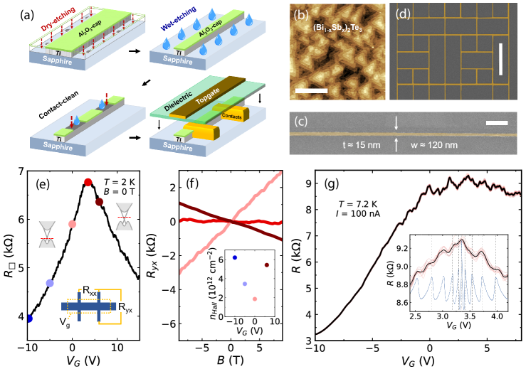
Figure 1a shows a schematic of our top-down fabrication process. After the patterning with electron-beam (EB) lithography, dry-etching with Ar plasma is performed first to remove unnecessary parts of the BST/Al2O3 film. Subsequently, a chemical wet-etching with diluted H2O2/H2SO4 is carried out to remove damaged edges of the remaining BST to obtain NWs with a smooth edge. Next, the contact areas are exposed by employing EB lithography and removing the Al2O3 capping layer in heated Transene Type-D etchant; the exposed BST surface is then cleaned in diluted HCl and further by low-power Ar plasma in the metallization machine. The electrodes (either Pt/Au or Nb) are sputter-deposited in UHV. For our top-gate devices, we deposited a 50-nm-thick Al2O3-dielectric in the ALD machine and then fabricated the top-gate electrode with Pt/Au. Further details are described in the Methods section.
An atomic-force-microscopy (AFM) image of the surface of a typical pristine BST thin film used in our work is shown in Figure 1b. The well-developed terraces with the step height of 1 nm are a signature of high-quality epitaxial growth. As shown in Figure 1c, etched NWs can have arbitrary channel lengths with only small fluctuations in the width; the NW pictured here had the width 120 20 nm and the thickness 15 2 nm. With such dimensions, the quasi-1D subbands in the NW have an energy spacing of several meV 32, 13, 2. Figure 1d showcases that this approach allows to fabricate advanced geometries and arbitrary complex networks of bulk-insulting TINWs.
To characterize the properties of the BST film after the NW-fabrication process, we fabricated a relatively wide “ribbon” with a width = 500 nm, for which the Hall measurement is possible (note, in contrast, the Hall voltage would not appear in a strictly 1D system, and hence the interpretation of the Hall measurement is difficult in a quasi-1D system). The sheet-resistance of such a ribbon sample at 2 K is shown in Figure 1e as a function of the gate voltage , and Figure 1f shows the magnetic-field dependence of the Hall resistance of this ribbon sample for three values. The peak in corroborated with a sign change in gives clear evidence for the CNP-crossing and the bulk-insulating nature of the ribbon after the NW-fabrication process. The and data for = 0 V give the hole density = cm-2 and the mobility = 600 cm2/Vs, which are close to the values of the pristine material (Supplementary Figure S2). These results demonstrate that our NW-fabrication process causes little degradation in bulk-insulating BST.
Once the width of the ribbon is reduced to the “nanowire” regime, which is typically realized for 250 nm, the subband physics starts to show up 13, 2. One characteristic feature is the -dependent oscillation of the NW resistance . Such a behavior observed in a 150 nm NW (the device picture is shown in Supplementary Figure S4) is presented in Figure 1g, where thin red lines show the results of 10 uni-directional -sweeps and the thick black line shows their average. One can see that the pattern of the oscillations is disordered but is essentially reproducible. As shown in the inset of Figure 1g for a smaller range near the CNP, reproducible maxima and minima with a characteristic quadratic spacing can be identified. This feature has been elucidated in VLS-grown NWs 13 to stem from the regular change in the density of states that occurs when the chemical potential crosses the edge of the quantum-confined subbands. The expected positions of the maxima in can be calculated by using the gate capacitance = 55 pF/m estimated from a simple electrostatic model (see Supporting Information), and the theoretically expected positions are in reasonable agreement with the experimentally observed peaks near the CNP. For this NW, we have also estimated the mobility from the data and found no evidence for degradation (see Supporting Information).
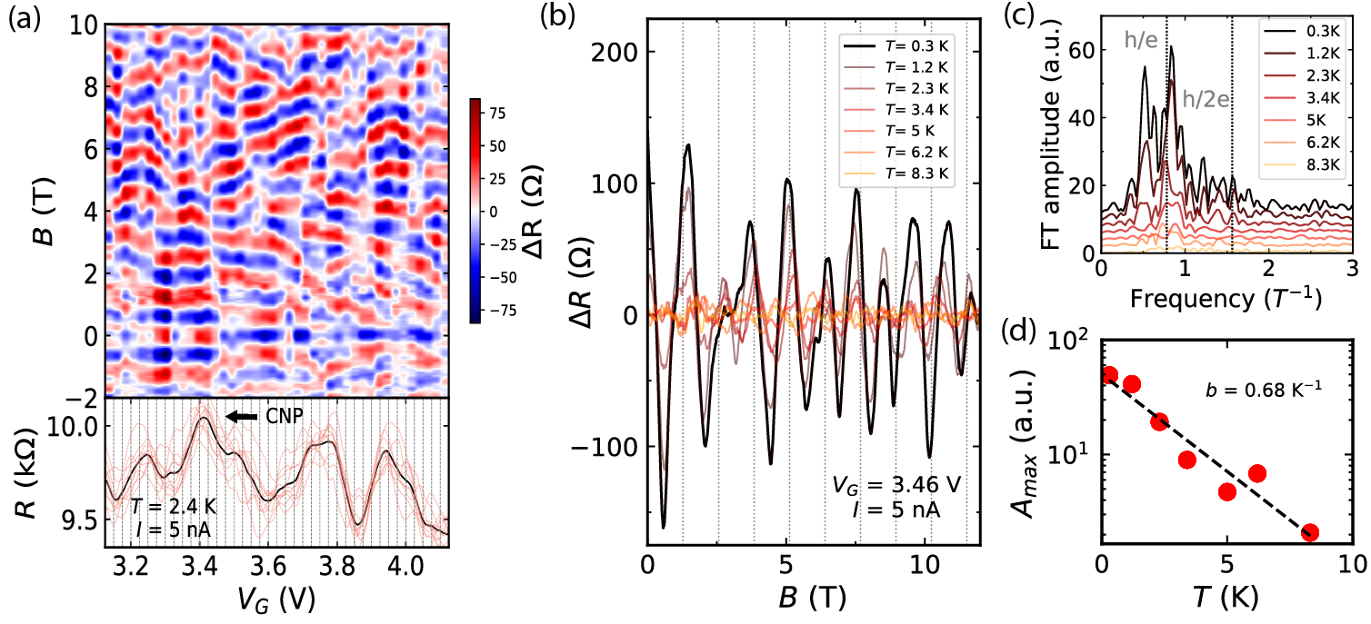
It is well known 10, 33, 11, 15, 12, 20, 34, 19 that the quantum-confined subbands in TINWs also give rise to oscillations of in parallel magnetic fields with the period of the flux quantum . This phenomenon is called Aharonov-Bohm (AB) oscillations, because it stems from the AB phase affecting the quantized angular momentum of the subbands 35, 36. Since the application of leads to oscillations in as well, the AB oscillations in TINWs are known to present -dependent -phase shifts 15, 12, 37, 34. To observe this interplay between and , we applied a magnetic field parallel to the NW at various values changed with small steps, and traced the dependence of on and . Figure 2a (upper panel) shows a color mapping of in the plane of vs , where with a smooth background; the lower panel presents the behavior at = 0 T for the same gating range, showing that several subband crossings are occurring in this range. Although the periodicity in is often distorted in Figure 2a, the approximate period of the -dependent oscillations, 1.3 T, is consistent with for the cross-section of this NW (150 30 nm2). One can see that sudden -phase shifts occur at several values, and the occurrence of the sudden phase shifts seen in the upper panel is roughly correlated with the peak-dip features in the lower panel (see Supplementary Figure S6 for additional plots). Ideally, a regular checker-board pattern (Supplementary Figure S5) is expected in the plane of vs ; however, experimentally the pattern is always distorted 15, 12, 20, 34 which may stem from orbital effects, subband splitting due to gating 9, or disorder 37.
In our NW, the decay of the AB oscillations with increasing temperature is exponential 38, 12, 34 rather than a power law 10, suggesting an approximate phase coherence around the perimeter of the NW 38, 12, 34. Figure 2b shows measured in the temperature range of 0.3–8.3 K near CNP at = 3.46 V, and the Fourier transform (FT) of these data are shown in Figure 2c. One can see that the dominant oscillation frequency corresponds to the AB oscillations with the period , and the Altshuler-Aronov-Spivak (AAS) oscillations 39 with period is essentially absent 10, which is typical for a short TINW 34. Figure 2d demonstrates that the decay of the maximum FT amplitude with temperature is well described by an exponential behavior, , which has been interpreted to originate from the disorder-induced thermal length that changes as 38. By putting with the perimeter length (= 360 nm in the present NW), = 0.68 K-1 obtained in our analysis corresponds to 0.53 m at 1 K, which is shorter than that in VLS-grown TINWs 38, 12, 34.
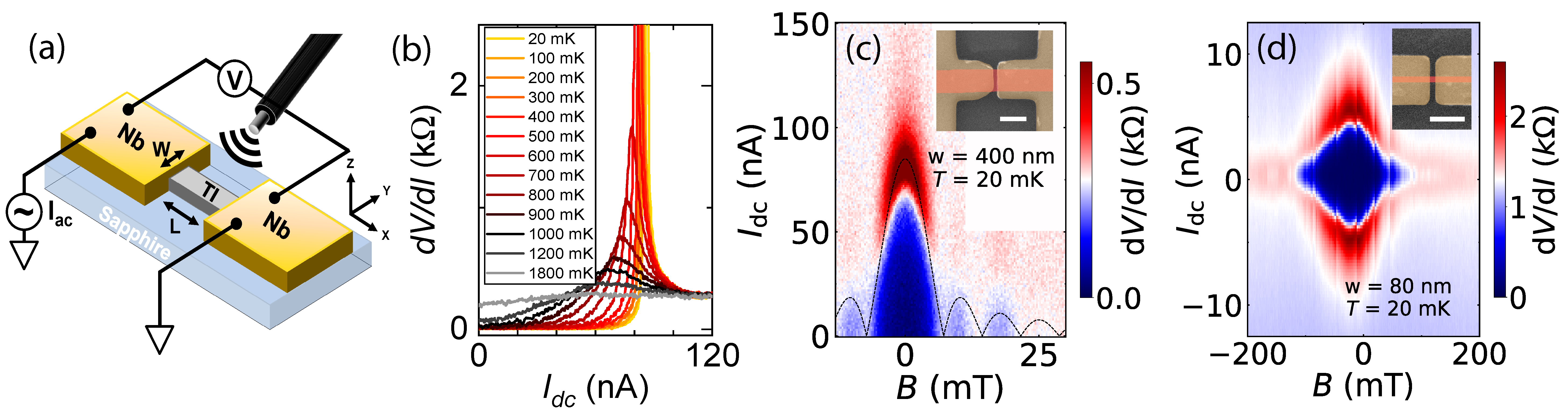
To see if our top-down fabricated TINWs can be a viable platform to search for Majorana bound states 6, 7, we have fabricated Josephson junctions (JJs) consisting of Nb electrodes contacting the NW with a small separation ( nm). To ensure bulk-insulation in the NW, BST films with a particularly low carrier concentration were chosen for the NW-fabrication (Supplementary Figures S7 and S8). The JJ devices, schematically depicted in Figure 3a, are measured in a quasi-four-terminal configuration and can be exposed to rf radiation to study their Shapiro response.
Figure 3b shows that in our Junction 1, which had a = 400 nm TI ribbon (see the SEM-image in Figure 3c inset), a well-developed critical current is observed at 20 mK but diminishes at 1 K, and at 1.8 K there is almost no sign of superconductivity. The temperature dependence of allows for an estimate of the interface transparency of the JJ, as was done in similar JJs 40, 17, which gives a relatively low transparency of 0.5 (see Supporting Information). A different method of estimating the interface transparency based on the excess current observed in the - curve 41 also gives (see Supporting Information). Hence, there is room for improving the JJ properties by preparing a more transparent interface, which we leave for future works.
When a perpendicular magnetic field is applied to a usual JJ, the creation of Josephson vortices in the junction leads to the appearance of a Fraunhofer pattern in the -dependence of 42. Hence, the Fraunhofer pattern is an indication of the phase winding along the width of the junction, which is not expected when the JJ is formed on a NW having no degree of freedom along the width of the junction. Indeed, whereas the Junction 1 made on a 400-nm-wide ribbon shows a Fraunhofer pattern (Figure 3c), the Junction 2 made on a 80-nm-wide NW just presents a monotonic decay of with (Figure 3d). To the best of our knowledge, our Junction 2 is the first successful JJ made on a TINW having such a narrow width of 80 nm. For Junction 1, the effective area m2 indicated by the periodicity of the Fraunhofer pattern (9 mT) is consistent with the geometrical area considering the flux focusing effect 43, 44.
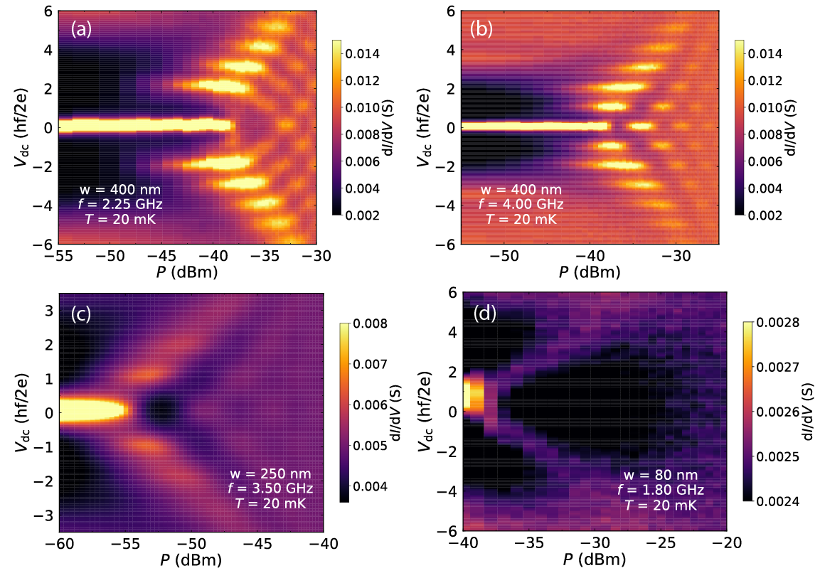
We have also studied the behavior of the Shapiro steps in our JJs under rf irradiation. Figure 4 shows color mappings of the differential conductance d/d measured in three JJs as a function of the rf power and the applied dc bias normalized by with the rf frequency; in this type of plots, the horizontal lines appearing at correspond to Shapiro steps with index . Figures 4a and 4b show the Shapiro response of Junction 1 (made on a 400-nm-wide TI ribbon) at 20 mK for 2.25 and 4 GHz, respectively. The 2.25-GHz data lack the = 1 step, while the 4-GHz data present all integer steps. At an intermediate frequency of 3 GHz, the 1st Shapiro step was partially observed (Supplementary Figure S11). The missing 1st Shapiro step has been reported before for TI-based JJs 45, 46, 40, 47, 48, 44, 21 and was interpreted to be possible evidence for Majorana bound states which endow -periodicity to the JJ 49. However, the Shapiro response alone can never give conclusive evidence for Majorana bound states because other mechanisms of nontopological origin can also cause the 1st Shapiro step to become missing 50, 51, 52, 21. Hence, our observation just demonstrates that our top-down fabrication process does not adversely affect the SC proximity effect in TIs and can be useful for future studies of Majorana bound states.
If one interprets the missing 1st Shapiro step to be due to a -periodic component in the Josephson response 53, the characteristic crossover frequency for the appearance of the 1st Shapiro step can be linked to the amplitude of the -periodic current via with the normal-state resistance of the junction 45. For our Junction 1, we infer 3 GHz, which gives 26 nA and 0.36.
Of particular interest is how such a Shapiro response changes when the TI-part is narrowed into the NW regime 54, 55, 44, 21, but our Shapiro-measurement setup was not good enough for this purpose. For our Junction 3 ( = 250 nm), 3.5 GHz was the lowest at which we could observe Shapiro steps, and the = 1 step was present (Figure 4c). In Junction 2 which had the narrowest NW ( = 80 nm), we detected no Shapiro response at any frequency (Figure 4d). This result tells us that the electromagnetic coupling between the TINW and the microwave antenna should be improved, which is beyond the scope of this study. Once a stronger coupling is achieved, it would be interesting to clarify the effect of parallel magnetic fields on the TINW-based JJ to detect the possible generation of Majorana bound states 6, 21. Trying to detect the microwave emission from a voltage-biased JJ 56, 57 would also be a promising future direction for proximitized TINWs.
In conclusion, we established a top-down fabrication process for bulk-insulating TINWs that are etched from MBE-grown (Bi1-xSbx)2Te3 thin films while maintaining the pristine material’s properties. In normal-state transport experiments, characteristic resistance oscillations as a function of both gate voltage and parallel magnetic field are observed, giving evidence that the characteristic TI-subband physics manifests itself in our NWs. We further demonstrate that it is possible to study the superconducting proximity effect in these TINWs by fabricating Josephson junctions with ex-situ prepared Nb contacts, providing the foundation for future devices to investigate Majorana bound states. The process established here is based on widely available clean-room technologies, benefits from the well-controlled properties of high-quality MBE-grown thin films, and enables flexible design of NW geometries. Hence, the results presented here will widen the opportunities for research using mesoscopic topological devices.
1 Methods
1.1 Material growth and device fabrication
The (Bi1-xSbx)2Te3 thin films were grown on sapphire (0001) substrates by co-evaporation of high-purity Bi, Sb, and Te in an ultra-high-vacuum MBE chamber. The flux of Bi and Sb was optimized to obtain the most bulk-insulating films which was achieved with a ratio of 1:6.8. The average thicknesses of the thin films, measured with AFM, were nominally in the range of 15–30 nm. Within minutes after taking the films out of the MBE chamber, they were capped with a 3-nm-thick Al2O3 layer grown by atomic layer deposition (ALD) at 80 using a Ultratec Savannah S200. The carrier density and the mobility of the pristine films were extracted from Hall measurements performed at 2 K using a Quantum Design PPMS. Gate-tunable multi-terminal NW devices were fabricated using the top-down process, the outline of which was described in the main text. After defining the nanowire shape with EB lithography, the film was first dry-etched using low-power Ar plasma. This process can degrade the TI-side-surfaces and can leave residual hard-to-remove resist patches behind. Therefore, a (H2SO4:H2O2):H2O (1:3):8 aqueous solution was used to remove the residual resist as well as the damaged material from the sidewalls of the NWs. To ensure a more controlled etch, the etchant and DI water were cooled to 8 ∘C. A second step of EB lithography was employed to form two kinds of contacts. Normal-state measurements were made with metal contacts that connect to the remaining BST-leads next to the NW to have an enlarged contact area and to avoid unintentional contact-doping in the NW. On the other hand, superconducting contacts were placed in a regular Josephson junction layout directly on top of the NW. In the contact areas, the Al2O3 capping layer was removed by aluminum etchant (Transene Type-D) heated to 50 ∘ C. After ex-situ and in-situ contact cleaning in diluted HCl:H2O (1:10) and low-power Ar-plasma in the sputtering machine just before metallization, 5/45 nm Pt/Au contacts or 45/5 nm Nb/Au contacts were deposited by UHV-sputtering. Non-superconducting devices were capped with a 50-nm-thick Al2O3 dielectric grown by ALD at 80 ∘C, after which a 5/40 nm Pt/Au top gate was sputter-deposited. In devices with superconducting contacts, the quality of the induced gap was very sensitive to the interface conditions, and for that reason, all the steps between the removal of the Al2O3 capping layer and the contact deposition were carried out in a N2-atmosphere using a Sigma-Aldrich Atmosbag to minimize oxide formation from exposure to air 31. The final dimensions of the devices were determined with scanning electron microscopy.
1.2 Transport measurements
Non-superconducting transport measurements were performed in a 3He cryostat (Oxford Instrument Heliox VL), a system that can be operated in a temperature range from 0.25 K to 30 K and in magnetic fields up to 13 T. A top-mounted RC-filter box is used to reduce the electromagnetic noise. Superconducting transport measurements are carried out in a dry dilution refrigerator (Oxford Instruments TRITON 300) equipped with a 3-axis vector magnet. In this system, low temperature electronic filtering includes microwave filters, low-pass resistor-capacitor filters and copper-powder filters to reduce electron heating by high-frequency noise. Voltages were measured in a standard four-terminal configuration with a low-frequency lock-in technique with 13.37 Hz using lock-in amplifiers (NF Corporation LI5645, Stanford Research Systems SR530 and SR830). To apply dc gate voltages or dc bias currents, a Keithley 2450 in combination with a 1-G resistor was used. For measurements, a small ac bias current was generated by using the output voltage of a lock-in amplifier in combination with a 10-M resistor and added on top of a larger dc current bias. The resulting differential voltage is measured with a lock-in technique.
2 Author Information
2.1 ORCID
Matthias Rößler: 0000-0001-9911-2835
Felix Münning: 0000-0003-0193-3542
Alexey A. Taskin: 0000-0002-2731-761X
Gertjan Lippertz: 0000-0002-4061-7027
Anjana Uday: 0000-0002-9719-0458
Henry F. Legg: 0000-0003-0400-5370
Yoichi Ando: 0000-0002-3553-3355
2.2 Notes
The authors declare no competing financial interest.
We are grateful for valuable discussions and support at various stages of this work from A. Rosch, E. Bocquillon, D. Rosenbach, O. Breunig, J. Feng, J. Schluck, N. Zapata, L. Hamdan and T. Zent. This project has received funding from the European Research Council (ERC) under the European Union’s Horizon 2020 research and innovation programme (grant agreement No 741121 [Y.A.]. It was also funded by the Deutsche Forschungsgemeinschaft (DFG, German Research Foundation) under CRC 1238 - 277146847 (Subprojects A04 and B01) [Y.A., A.T.] as well as under Germany’s Excellence Strategy - Cluster of Excellence Matter and Light for Quantum Computing (ML4Q) EXC 2004/1 - 390534769 [Y.A.]. This work was also supported by the Georg H. Endress Foundation [H.F.L.]. G.L. acknowledges the support by the KU Leuven BOF and Research Foundation Flanders (FWO, Belgium), file No. 27531 and No. 52751.
The Supporting Information is available free of charge at ….
Properties of BST before and after the NW-fabrication process, Gate-tunable nanowire device image and wiring, Gate-voltage dependent resistance oscillations in TINW, Estimation of the mobility in nanowires, -phase shift in the Aharonov-Bohm oscillations, Properties of the pristine BST films used for the Josephson junction devices, Temperature dependence of the critical current in Junction 1, Characteristic parameters of the Josephson-junction devices, Shapiro step data for Junction 1 at = 3 GHz.
TOC image:
![[Uncaptioned image]](/html/2302.01209/assets/TOC.png)
References
- Ando 2013 Ando, Y. Topological insulator materials. Journal of the Physical Society of Japan 2013, 82
- Breunig and Ando 2022 Breunig, O.; Ando, Y. Opportunities in topological insulator devices. Nature Reviews Physics 2022, 4, 184–193
- Sato and Ando 2017 Sato, M.; Ando, Y. Topological superconductors: a review. Reports on Progress in Physics 2017, 80, 076501
- Fu and Kane 2008 Fu, L.; Kane, C. L. Superconducting Proximity Effect and Majorana Fermions at the Surface of a Topological Insulator. Phys. Rev. Lett. 2008, 100, 96407
- Nayak et al. 2008 Nayak, C.; Stern, A.; Freedman, M.; Das Sarma, S. Non-Abelian anyons and topological quantum computation. Reviews of Modern Physics 2008, 80, 1083–1159
- Cook and Franz 2011 Cook, A.; Franz, M. Majorana fermions in a topological-insulator nanowire proximity-coupled to an s-wave superconductor. Phys. Rev. B 2011, 84, 201105
- Legg et al. 2021 Legg, H. F.; Loss, D.; Klinovaja, J. Majorana bound states in topological insulators without a vortex. Phys. Rev. B 2021, 104, 165405
- Legg et al. 2022 Legg, H. F.; Loss, D.; Klinovaja, J. Superconducting diode effect due to magnetochiral anisotropy in topological insulators and Rashba nanowires. Phys. Rev. B 2022, 106, 104501
- Legg et al. 2022 Legg, H. F.; Rößler, M.; Münning, F.; Fan, D.; Breunig, O.; Bliesener, A.; Lippertz, G.; Uday, A.; Taskin, A. A.; Loss, D.; Klinovaja, J.; Ando, Y. Giant magnetochiral anisotropy from quantum-confined surface states of topological insulator nanowires. Nature Nanotechnology 2022,
- Peng et al. 2010 Peng, H.; Lai, K.; Kong, D.; Meister, S.; Chen, Y.; Qi, X.-L.; Zhang, S.-C.; Shen, Z.-X.; Cui, Y. Aharonov-Bohm interference in topological insulator nanoribbons. Na.t Mater. 2010, 9, 225–229
- Hong et al. 2014 Hong, S. S.; Zhang, Y.; Cha, J. J.; Qi, X.-L.; Cui, Y. One-Dimensional Helical Transport in Topological Insulator Nanowire Interferometers. Nano Letters 2014, 14, 2815–2821
- Jauregui et al. 2016 Jauregui, L. A.; Pettes, M. T.; Rokhinson, L. P.; Shi, L.; Chen, Y. P. Magnetic field-induced helical mode and topological transitions in a topological insulator nanoribbon. Nature Nanotechnology 2016, 11, 345–351
- Münning et al. 2021 Münning, F.; Breunig, O.; Legg, H. F.; Roitsch, S.; Fan, D.; Rößler, M.; Rosch, A.; Ando, Y. Quantum confinement of the Dirac surface states in topological-insulator nanowires. Nat. Commun. 2021, 12, 1–6
- Liu et al. 2019 Liu, P.; Williams, J. R.; Cha, J. J. Topological nanomaterials. Nature Reviews Materials 2019, 4, 479–496
- Cho et al. 2015 Cho, S.; Dellabetta, B.; Zhong, R.; Schneeloch, J.; Liu, T.; Gu, G.; Gilbert, M. J.; Mason, N. Aharonov-Bohm oscillations in a quasi-ballistic three-dimensional topological insulator nanowire. Nature Communications 2015, 6, 1–5
- Cho et al. 2016 Cho, S.; Zhong, R.; Schneeloch, J. A.; Gu, G.; Mason, N. Kondo-like zero-bias conductance anomaly in a three-dimensional topological insulator nanowire. Scientific Reports 2016, 6, 21767
- Bai et al. 2022 Bai, M.; Wei, X.-K.; Feng, J.; Luysberg, M.; Bliesener, A.; Lippertz, G.; Uday, A.; Taskin, A. A.; Mayer, J.; Ando, Y. Proximity-induced superconductivity in topological-insulator nanowires. Communications Materials 2022, 3, 20
- Kölzer et al. 2020 Kölzer, J.; Rosenbach, D.; Weyrich, C.; Schmitt, T. W.; Schleenvoigt, M.; Jalil, A. R.; Schüffelgen, P.; Mussler, G.; IV, V. E. S.; Grützmacher, D.; Lüth, H.; Schäpers, T. Phase-coherent loops in selectively-grown topological insulator nanoribbons. Nanotechnology 2020, 31, 325001
- Rosenbach et al. 2020 Rosenbach, D.; Oellers, N.; Jalil, A. R.; Mikulics, M.; Kölzer, J.; Zimmermann, E.; Mussler, G.; Bunte, S.; Grützmacher, D.; Lüth, H.; Schäpers, T. Quantum Transport in Topological Surface States of Selectively Grown Nanoribbons. Advanced Electronic Materials 2020, 6, 2000205
- Ziegler et al. 2018 Ziegler, J.; Kozlovsky, R.; Gorini, C.; Liu, M.-H.; Weishäupl, S.; Maier, H.; Fischer, R.; Kozlov, D. A.; Kvon, Z. D.; Mikhailov, N.; Others, Probing spin helical surface states in topological HgTe nanowires. Phy. Rev. B 2018, 97, 35157
- Fischer et al. 2022 Fischer, R.; Picó-Cortés, J.; Himmler, W.; Platero, G.; Grifoni, M.; Kozlov, D. A.; Mikhailov, N. N.; Dvoretsky, S. A.; Strunk, C.; Weiss, D. -periodic supercurrent tuned by an axial magnetic flux in topological insulator nanowires. Phys. Rev. Research 2022, 4, 13087
- Zhang et al. 2011 Zhang, J.; Chang, C.-Z.; Zhang, Z.; Wen, J.; Feng, X.; Li, K.; Liu, M.; He, K.; Wang, L.; Chen, X.; Xue, Q.-K.; Ma, X.; Wang, Y. Band structure engineering in ternary topological insulators. Nature Communications 2011, 2, 574
- Kong et al. 2011 Kong, D.; Chen, Y.; Cha, J. J.; Zhang, Q.; Analytis, J. G.; Lai, K.; Liu, Z.; Hong, S. S.; Koski, K. J.; Mo, S.-K.; Hussain, Z.; Fisher, I. R.; Shen, Z.-X.; Cui, Y. Ambipolar field effect in the ternary topological insulator by composition tuning. Nature Nanotechnology 2011, 6, 705–709
- Yang et al. 2014 Yang, F.; Taskin, A. A.; Sasaki, S.; Segawa, K.; Ohno, Y.; Matsumoto, K.; Ando, Y. Top gating of epitaxial topological insulator thin films. Applied Physics Letters 2014, 104, 161614
- Yoshimi et al. 2015 Yoshimi, R.; Tsukazaki, A.; Kozuka, Y.; Falson, J.; Takahashi, K. S.; Checkelsky, J. G.; Nagaosa, N.; Kawasaki, M.; Tokura, Y. Quantum Hall effect on top and bottom surface states of topological insulator films. Nature Communications 2015, 6, 6627
- Yang et al. 2015 Yang, F.; Taskin, A. A.; Sasaki, S.; Segawa, K.; Ohno, Y.; Matsumoto, K. Dual-Gated Topological Insulator Thin-Film Device for Efficient Fermi-Level Tuning. ACS Nano 2015, 4050–4055
- Koirala et al. 2015 Koirala, N.; Brahlek, M.; Salehi, M.; Wu, L.; Dai, J.; Waugh, J.; Nummy, T.; Han, M.-G.; Moon, J.; Zhu, Y.; Dessau, D.; Wu, W.; Armitage, N. P.; Oh, S. Record Surface State Mobility and Quantum Hall Effect in Topological Insulator Thin Films via Interface Engineering. Nano Letters 2015, 15, 8245–8249
- Taskin et al. 2017 Taskin, A. A.; Legg, H. F.; Yang, F.; Sasaki, S.; Kanai, Y.; Matsumoto, K.; Rosch, A.; Ando, Y. Planar Hall effect from the surface of topological insulators. Nature Communications 2017, 8, 1340
- Lang et al. 2012 Lang, M.; He, L.; Xiu, F.; Yu, X.; Tang, J.; Wang, Y.; Kou, X.; Jiang, W.; Fedorov, A. V.; Wang, K. L. Revelation of Topological Surface States in Thin Films by In Situ Al Passivation. ACS Nano 2012, 6, 295–302
- Ngabonziza et al. 2015 Ngabonziza, P.; Heimbuch, R.; de Jong, N.; Klaassen, R. A.; Stehno, M. P.; Snelder, M.; Solmaz, A.; Ramankutty, S. V.; Frantzeskakis, E.; van Heumen, E.; Koster, G.; Golden, M. S.; Zandvliet, H. J. W.; Brinkman, A. In situ spectroscopy of intrinsic topological insulator thin films and impact of extrinsic defects. Phys. Rev. B 2015, 92, 35405
- Volykhov et al. 2018 Volykhov, A. A.; Sa, J.; Batuk, M.; Callaert, C.; Hadermann, J.; Sirotina, A. P.; Neudachina, V. S.; Belova, A. I.; Vladimirova, N. V.; Tamm, M. E. Can surface reactivity of mixed crystals be predicted from their counterparts ? A case study. Journal of Materials Chemistry C 2018, 6, 8941–8949
- Cook et al. 2012 Cook, A. M.; Vazifeh, M. M.; Franz, M. Stability of Majorana fermions in proximity-coupled topological insulator nanowires. Physical Review B - Condensed Matter and Materials Physics 2012, 86, 1–17
- Xiu et al. 2011 Xiu, F.; He, L.; Wang, Y.; Cheng, L.; Chang, L.-t.; Lang, M.; Huang, G.; Kou, X.; Zhou, Y.; Jiang, X.; Chen, Z.; Zou, J.; Shailos, A.; Wang, K. L. Manipulating surface states in topological insulator nanoribbons. Nature Nanotechnology 2011, 6
- Kim et al. 2020 Kim, H.-S.; Hwang, T.-H.; Kim, N.-H.; Hou, Y.; Yu, D.; Sim, H.-S.; Doh, Y.-J. Adjustable Quantum Interference Oscillations in Sb-Doped Bi2Se3 Topological Insulator Nanoribbons. ACS Nano 2020, 14, 14118–14125
- Zhang and Vishwanath 2010 Zhang, Y.; Vishwanath, A. Anomalous Aharonov-Bohm Conductance Oscillations from Topological Insulator Surface States. Physical Review Letters 2010, 105, 206601
- Bardarson et al. 2010 Bardarson, J. H.; Brouwer, P. W.; Moore, J. E. Aharonov-Bohm Oscillations in Disordered Topological Insulator Nanowires. Physical Review Letters 2010, 105, 156803
- Sacksteder and Wu 2016 Sacksteder, V. E.; Wu, Q. Quantum interference effects in topological nanowires in a longitudinal magnetic field. Phys. Rev. B 2016, 94, 205424
- Dufouleur et al. 2013 Dufouleur, J.; Veyrat, L.; Teichgräber, A.; Neuhaus, S.; Nowka, C.; Hampel, S.; Cayssol, J.; Schumann, J.; Eichler, B.; Schmidt, O. G.; Büchner, B.; Giraud, R. Quasiballistic Transport of Dirac Fermions in a Nanowire. Phys. Rev. Lett. 2013, 110, 186806
- Al’tshuler et al. 1981 Al’tshuler, B.; Aronov, A.; Spivak, B. The Aharonov-Bohm Effect in Disordered Conductors. JETP Lett. 1981, 33, 94
- Schüffelgen et al. 2019 Schüffelgen, P. et al. Selective area growth and stencil lithography for in situ fabricated quantum devices. Nature Nanotechnology 2019, 14, 825–831
- Flensberg et al. 1988 Flensberg, K.; Hansen, J. B.; Octavio, M. Subharmonic energy-gap structure in superconducting weak links. Phys. Rev. B 1988, 38, 8707–8711
- Gross et al. 2016 Gross, R.; Marx, A.; Deppe, F. Applied superconductivity: Josephson effect and superconducting electronics; De Gruyter, 2016
- Ghatak et al. 2018 Ghatak, S.; Breunig, O.; Yang, F.; Wang, Z.; Taskin, A. A.; Ando, Y. Anomalous Fraunhofer patterns in gated Josephson junctions based on the bulk-insulating topological insulator BiSbTeSe2. 2018, 1–13
- Rosenbach et al. 2021 Rosenbach, D.; Schmitt, T. W.; Schüffelgen, P.; Stehno, M. P.; Li, C.; Schleenvoigt, M.; Jalil, A. R.; Mussler, G.; Neumann, E.; Trellenkamp, S.; Golubov, A. A.; Brinkman, A.; Grützmacher, D.; Schäpers, T. Reappearance of first Shapiro step in narrow topological Josephson junctions. Science Advances 2021, 7, eabf1854
- Wiedenmann et al. 2016 Wiedenmann, J.; Bocquillon, E.; Deacon, R. S.; Hartinger, S.; Herrmann, O.; Klapwijk, T. M.; Maier, L.; Gould, C.; Oiwa, A.; Ishibashi, K.; Tarucha, S.; Buhmann, H.; Molenkamp, L. W.; Ames, C.; Bru, C. 4 p -periodic Josephson supercurrent in HgTe-based topological Josephson junctions. 2016, 1–7
- Bocquillon et al. 2017 Bocquillon, E.; Deacon, R. S.; Wiedenmann, J.; Leubner, P.; Klapwijk, T. M.; Brüne, C.; Ishibashi, K.; Buhmann, H.; Molenkamp, L. W. Gapless Andreev bound states in the quantum spin Hall insulator HgTe. Nat. Nanotechnol. 2017, 12, 137–143
- Le Calvez et al. 2019 Le Calvez, K.; Veyrat, L.; Gay, F.; Plaindoux, P.; Winkelmann, C. B.; Courtois, H.; Sacépé, B. Joule overheating poisons the fractional ac Josephson effect in topological Josephson junctions. Commun. Phys. 2019, 2, 4
- de Ronde et al. 2020 de Ronde, B.; Li, C.; Huang, Y.; Brinkman, A. Induced Topological Superconductivity in a BiSbTeSe2-Based Josephson Junction. Nanomaterials 2020, 10, 794
- Fu and Kane 2008 Fu, L.; Kane, C. L. Superconducting Proximity Effect and Majorana Fermions at the Surface of a Topological Insulator. Phys. Rev. Lett. 2008, 100, 096407
- Chiu and Das Sarma 2019 Chiu, C.-K.; Das Sarma, S. Fractional Josephson effect with and without Majorana zero modes. Phys. Rev. B 2019, 99, 35312
- Dartiailh et al. 2021 Dartiailh, M. C.; Cuozzo, J. J.; Elfeky, B. H.; Mayer, W.; Yuan, J.; Wickramasinghe, K. S.; Rossi, E.; Shabani, J. Missing Shapiro steps in topologically trivial Josephson junction on InAs quantum well. Nature Communications 2021, 12, 78
- Zhang, P. and Mudi, S. and Pendharkar, M. and Lee, J. S. and Dempsey, C. P. and McFadden, A. P. and Harrington, S. D. and Dong, J. T. and Wu, H. and Chen, A. -H. and Hocevar, M. and Palmstrøm, C. J. and Frolov 2022 Zhang, P. and Mudi, S. and Pendharkar, M. and Lee, J. S. and Dempsey, C. P. and McFadden, A. P. and Harrington, S. D. and Dong, J. T. and Wu, H. and Chen, A. -H. and Hocevar, M. and Palmstrøm, C. J. and Frolov, S. M. Missing odd-order Shapiro steps do not uniquely indicate fractional Josephson effect. arXiv 2022,
- Dominguez et al. 2017 Dominguez, F.; Kashuba, O.; Bocquillon, E.; Wiedenmann, J.; Deacon, R. S.; Klapwijk, T. M.; Platero, G.; Molenkamp, L. W.; Trauzettel, B.; Hankiewicz, E. M. Josephson junction dynamics in the presence of - and -periodic supercurrents. Phys. Rev. B 2017, 95, 195430
- Laroche et al. 2019 Laroche, D.; Bouman, D.; van Woerkom, D. J.; Proutski, A.; Murthy, C.; Pikulin, D. I.; Nayak, C.; van Gulik, R. J. J.; Nygård, J.; Krogstrup, P.; Kouwenhoven, L. P.; Geresdi, A. Observation of the 4-periodic Josephson effect in indium arsenide nanowires. Nature Communications 2019, 10, 245
- Ueda et al. 2020 Ueda, K.; Matsuo, S.; Kamata, H.; Sato, Y.; Takeshige, Y.; Li, K.; Samuelson, L.; Xu, H.; Tarucha, S. Evidence of half-integer Shapiro steps originated from nonsinusoidal current phase relation in a short ballistic InAs nanowire Josephson junction. Phys. Rev. Research 2020, 2, 33435
- Deacon et al. 2017 Deacon, R. S.; Wiedenmann, J.; Bocquillon, E.; Domínguez, F.; Klapwijk, T. M.; Leubner, P.; Brüne, C.; Hankiewicz, E. M.; Tarucha, S.; Ishibashi, K.; Buhmann, H.; Molenkamp, L. W. Josephson Radiation from Gapless Andreev Bound States in HgTe-Based Topological Junctions. 2017, 021011, 1–7
- Kamata et al. 2018 Kamata, H.; Deacon, R. S.; Matsuo, S.; Li, K.; Jeppesen, S.; Samuelson, L.; Xu, H. Q.; Ishibashi, K.; Tarucha, S. Anomalous modulation of Josephson radiation in nanowire-based Josephson junctions. Phys. Rev. B 2018, 98, 41302