Fractional focusing peaks and collective dynamics in two-dimensional Fermi liquids
Abstract
Carrier transport in materials is often diffusive due to momentum-relaxing scattering with phonons and defects. Suppression of momentum-relaxing scattering can lead to the ballistic and hydrodynamic transport regimes, wherein complex non-Ohmic current flow patterns, including current vortices, can emerge. In the ballistic regime addressed here, transverse magnetic focusing is habitually understood in a familiar single-particle picture of carriers injected from a source, following ballistic cyclotron orbits and reaching a detector. We report on a distinctive nonlocal magnetoresistance phenomenon exclusive to fermions, in an enclosed mesoscopic geometry wherein transverse focusing magnetoresistance peaks also occur at values of the cyclotron diameter that are incommensurate with the distance between the source and detector. In low-temperature experiments and simulations using GaAs/AlGaAs heterostructures with high electron mobility, we show that the peaks occur independently of the location of the detector, and only depend on the source-drain separation. We reproduce the experimental findings using simulations of ballistic transport in both semiclassical and quantum-coherent transport models. The periodicity of magnetic field at which the peaks occur is matched to the lithographically defined device scale. It is found that, unlike in transverse magnetic focusing, the magnetoresistance structure cannot be attributed to any set of ordered single-particle trajectories but instead requires accounting for the collective dynamics of the fermion distribution and of all particle trajectories. The magnetoresistance is further associated with current flow vorticity, a collective phenomenon.
I Introduction
Ballistic carrier transport in solid-state systems occurs when charge carriers scatter predominantly against the device boundaries, rather than dissipating system momentum to the lattice or undergoing mainly electron-electron scattering [1, 2, 3, 4, 5, 6, 7]. Ballistic transport phenomena are often presented in terms of trajectories of single non-interacting particles, such as cyclotron orbits under an applied magnetic field . Here, we instead advance the conceptual picture of collective dynamics in ballistic transport [1, 2, 8, 9, 10, 11, 12]. We present a previously unreported periodic magnetoresistance structure occurring at low , in a confined transverse magnetic focusing (TMF) mesoscopic geometry in a high-mobility two-dimensional electron system (2DES) in a GaAs/AlGaAs heterostructure. We evince that the origin of the magnetoresistance structure cannot be traced to an ordered set of single-particle cyclotron orbits, and requires consideration of all trajectories in the device and of the collective dynamics of a fermion distribution including electron and hole excitations. Using experimental data and high-resolution kinetic simulations based on two complementary numerical schemes, we examine the factors that affect the magnetoresistance structure and lay out the essential conditions required for its manifestation. We show how the magnetoresistance correlates with current vorticity and backflow, collective properties significantly more complex than single-particle trajectories as well as harder to access experimentally.
In contrast to ballistic carrier transport, the more common diffusive transport in the solid state, governed by Ohm’s law, occurs when carrier mobility mean-free paths are limited by momentum-relaxing processes such as electron-phonon and electron-defect scattering which act to transfer momentum from the charge carriers to the lattice. Diffusive transport breaks down when this scattering becomes sufficiently weak and hence sufficiently long, as in two-dimensional particle systems in III-V heterostructures [1, 2, 13, 3, 4, 5, 14, 15, 16, 17, 18, 19, 20, 21, 22, 23], in graphene [24, 25, 26, 27, 28, 6, 7, 29, 30, 31, 11, 32, 33], in WTe2 [34, 35, 36, 37], or in delafossites such as (Pd/Pt)CoO2 [38, 39, 40, 41, 42, 43, 44, 45]. Not affecting total system momentum or carrier mobility or , momentum-conserving electron-electron scattering also exists, and at long it determines whether transport is ballistic or hydrodynamic. The ballistic regime occurs when electron-electron scattering is weak, the hydrodynamic regime occurs when it is strong, resulting in charge flow akin to a fluid. The hydrodynamic regime exemplifies collective transport and can lead to current vortex formation due to viscous drag that arises due to interactions [37, 1, 46, 11, 21, 31]. Vorticity in the ballistic regime is on the other hand surprising because there it occurs in the absence of interactions. Recent results in ballistic transport have challenged the single-particle trajectory notion which e.g. has been used to design ballistic devices [24, 47]. It has recently been shown that ballistic transport can produce complex current flow patterns that defy the single-particle trajectory notion and can lead to collective phenomena such as current vortices [1, 2, 9]. In this work, the experimental magnetoresistive phenomena find an origin in such collective ballistic dynamics. These are depicted in terms of current streamlines and voltage contour plots obtained from the kinetic simulations, further compared to a quantum-coherent transport model. In related context, other work has studied voltage and charge contour plots in mesoscopic geometries [48, 49], or imaged the contour plots by scanning gate microscopy [50].
The arrangement in which we study the magnetoresistance structure at low is a confined TMF geometry. TMF is a quintessentially ballistic magnetotransport technique [51, 13, 16, 52, 2, 53] that has been applied to the characterization of Fermi surfaces [51, 54, 16, 52, 25, 6, 32], the measurement of electron-electron scattering [2], the detection of composite fermions [55, 56], and the study of Andreev reflection [52] and spin-orbit interaction [57, 58].
II Device geometry and qualitative description
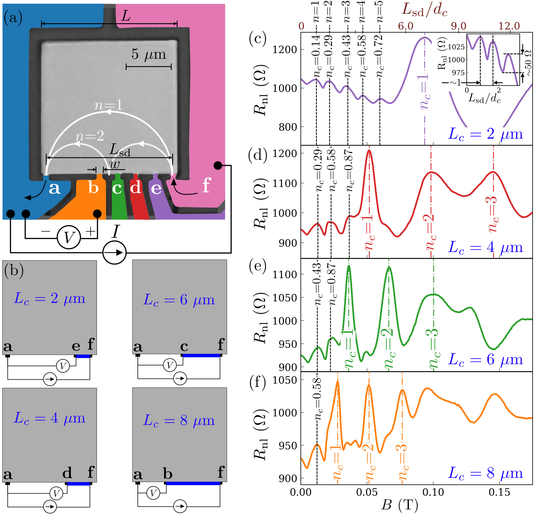
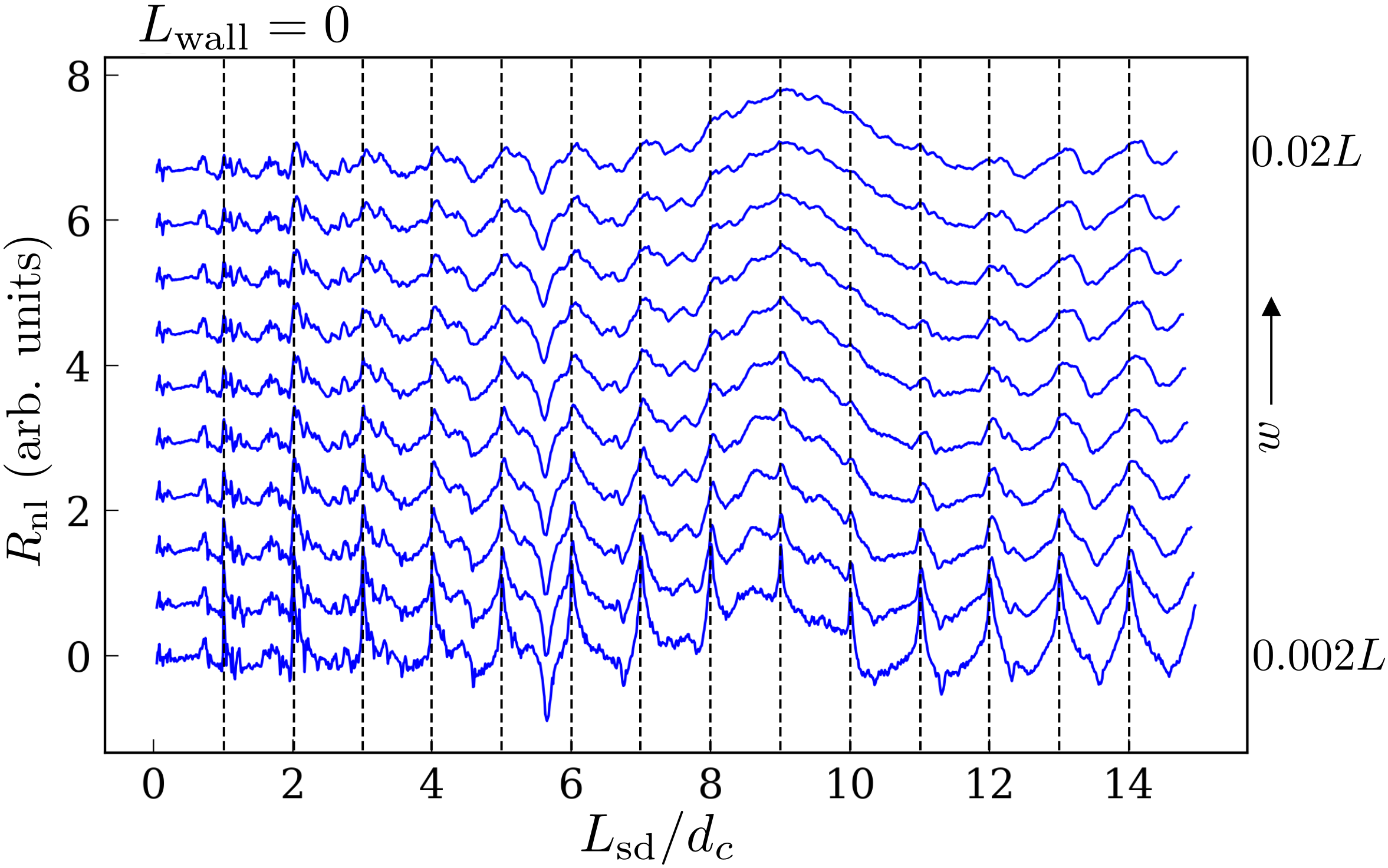
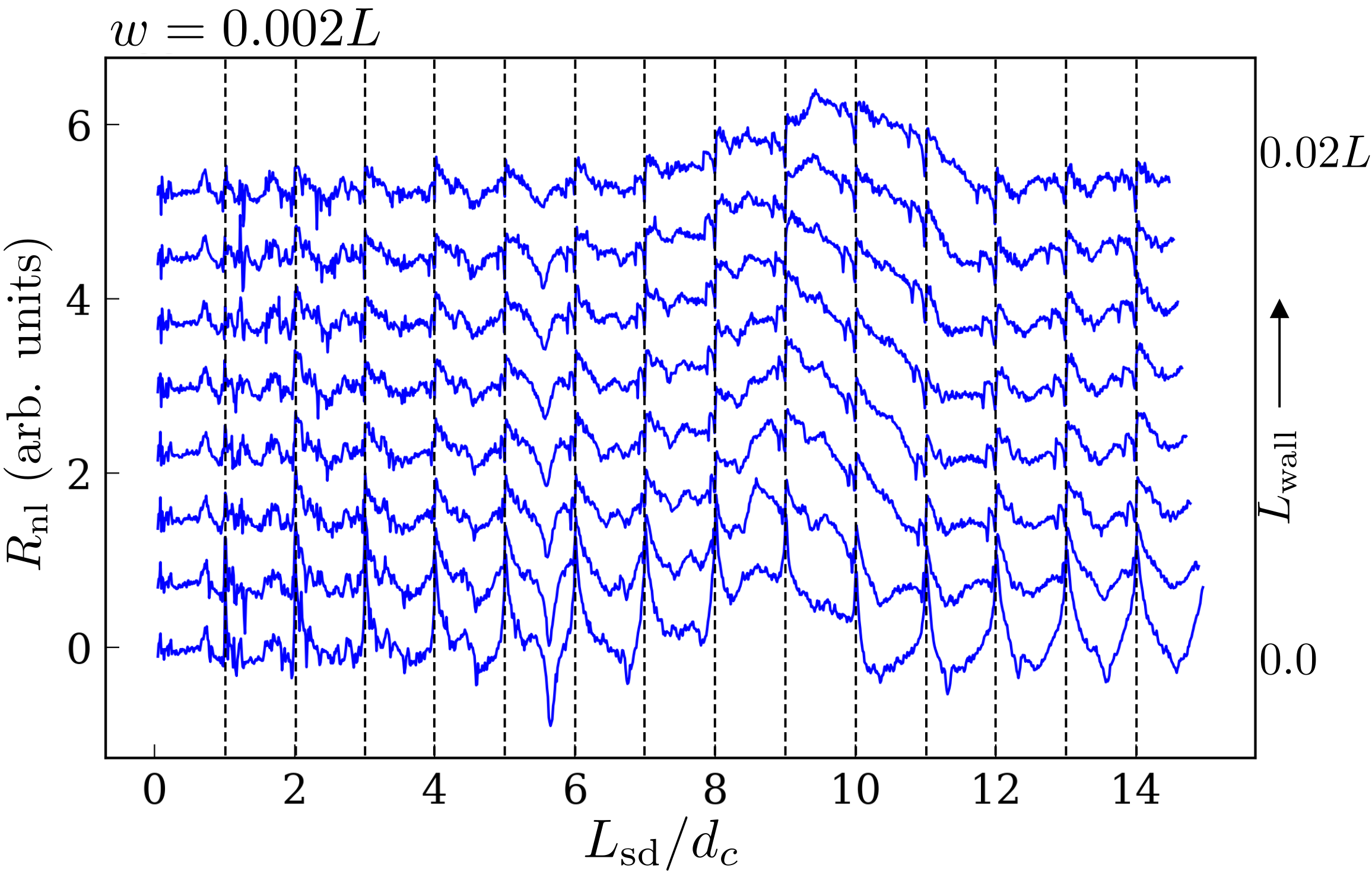
We consider a device geometry in a 2DES depicted in Fig. 1(a), a square defined by boundaries with internal edge length , and with current source and drain point contacts (PCs) of conducting widths placed near two corners along the same edge at center-to-center distance (necessarily ). Conventional current is injected into the device through the source PC (corresponding to injection of holes, referring to positive charges due to empty states below the Fermi contour [59, 60, 61, 62]), and extracted through the drain PC (corresponding to injection of electrons, filling states above the Fermi contour). In the device under consideration (Fig. 1(a)) we have , and . The scattering of electrons off the internal device boundaries is specular, as explained below. All measurements are performed at temperature 4.1 K. In the presence of a perpendicular magnetic field , carriers undergo semiclassical cyclotron orbits with cyclotron diameter , where denotes the elementary charge, the reduced Planck’s constant, and the Fermi wavevector. The 3-terminal nonlocal resistance is defined as the voltage measured between a detector PC and the drain PC divided by the injected current , where the detector PC is placed at a center-to-center distance from the source PC (Fig. 1(b)). reaches a positive peak whenever , with an integer. These integer focusing peaks, observed in Fig. 1(c-f) for , constitute TMF, and are a prototypical signature of ballistic transport. They can be understood in terms of single-particle ballistic trajectories of injected carriers which follow semiclassical cyclotron orbits and reach the detector PC after specular scattering events off the boundary between source and detector PC. Yet notably, the device geometry in Fig. 1(a) gives rise to an additional resonance condition visible as maxima in : , with an integer. This condition denotes a novel source-drain resonance, corresponding to of a carrier trajectory injected at the source PC fitting an integer number of times into (Fig. 1(a)). The matching maxima in occur at values of independent of the location of the detector PC between source and drain. Figures 1(c-f) show that the device manifests the source-drain resonances experimentally at lower , with distinct maxima in for that satisfy the resonance condition. The high-resolution simulations of ballistic transport likewise predict the resonances. The source-drain resonance peaks occur for all , and therefore, at effectively fractional . As will be described, unlike the TMF origin of the integer peaks, the fractional source-drain resonance peaks cannot be attributed to any particular particle trajectory: they only occur from the collective dynamics arising from a particle distribution. Further, while the integer peaks only require ballistic transport over the scale of , the fractional peaks require more stringent device-scale ballistic transport along with specular boundaries.
The experimental device in Fig. 1(a) is defined on a 2DES of very high electron hosted in a GaAs/AlGaAs heterostructure (Appendix A). Transport parameters of the 2DES are listed in Appendix A, including the long mean-free path at = 4.1 K. Hence , attesting to the very weak momentum-relaxing scattering which allows ballistic transport across the device. The Fermi wavelength nm shows there are spin-degenerate transverse modes injected through the PCs into the device and hence transport through the PCs is effectively classical. Further, the wet-etching process used to define the boundaries in the 2DES (Appendix A) results in specular scattering [1, 2, 17, 18, 20], thus allowing the fractional peaks to manifest in the device. The 15 m 15 m device in Fig. 1(a) features 6 PCs along the bottom boundary. Current is injected at the source PC at the right-end, and drained at the drain PC at the left-end. The intermediate PCs serve as detectors at m (Fig. 1(b)).
III Quantitative results and discussion
Figures 1(c-f) show the nonlocal resistance measured at K as a function of and . The integer peaks are conspicuous, e.g. for m the peak occurs at T and for m the peak occurs at T. Smaller clear peaks appear at lower , below , each with amplitude and at values of incommensurate with . We note that firstly, more fractional peaks appear for a detector closer to the source, with detector PCs at m detecting 5, 3, 2 and 1 fractional peaks respectively. This observation suggests that is a favorable condition for the fractional peaks to manifest. Secondly, the value of at which the fractional peaks occur is independent of (Fig. 1(c-f)). For example, we observe that the fractional peak occurs at the same for all detector PCs. In contrast, the integer peak occurs at that depends on . Finally, the periodicity of the fractional peaks is also independent of , unlike the integer peaks the periodicity of which depends on as (Fig. 1(c-f)).
We compare the experimental results to simulations of ballistic magnetotransport based on the collisionless Boltzmann transport equation in the limit (Appendix B),
| (1) |
where is the carrier probability distribution, are the spatial coordinates, is the angle on the (circular) Fermi contour and is the unit vector along the Fermi velocity. We solve Eq. 1 using two numerical schemes: a finite volume (FV) scheme where the distribution is solved for on a uniform grid of the coordinates, and a Monte-Carlo (MC) scheme where the trajectories of injected carriers are evolved by analytically computing their intersections with the device boundaries at each specular scattering event off the boundaries. The former is a “bulk” scheme, whose output is the distribution over the entire device, while the latter is a “boundary” scheme where the solution is confined to the device boundaries, and is therefore computationally faster than the bulk scheme. At the source PC, we impose where is the angle with respect to the normal to the device boundary, corresponding to injection of holes below the Fermi contour. Similarly, at the drain PC we impose , corresponding to injection of electrons above the Fermi contour [9, 1, 2, 59, 60, 61, 62].
.
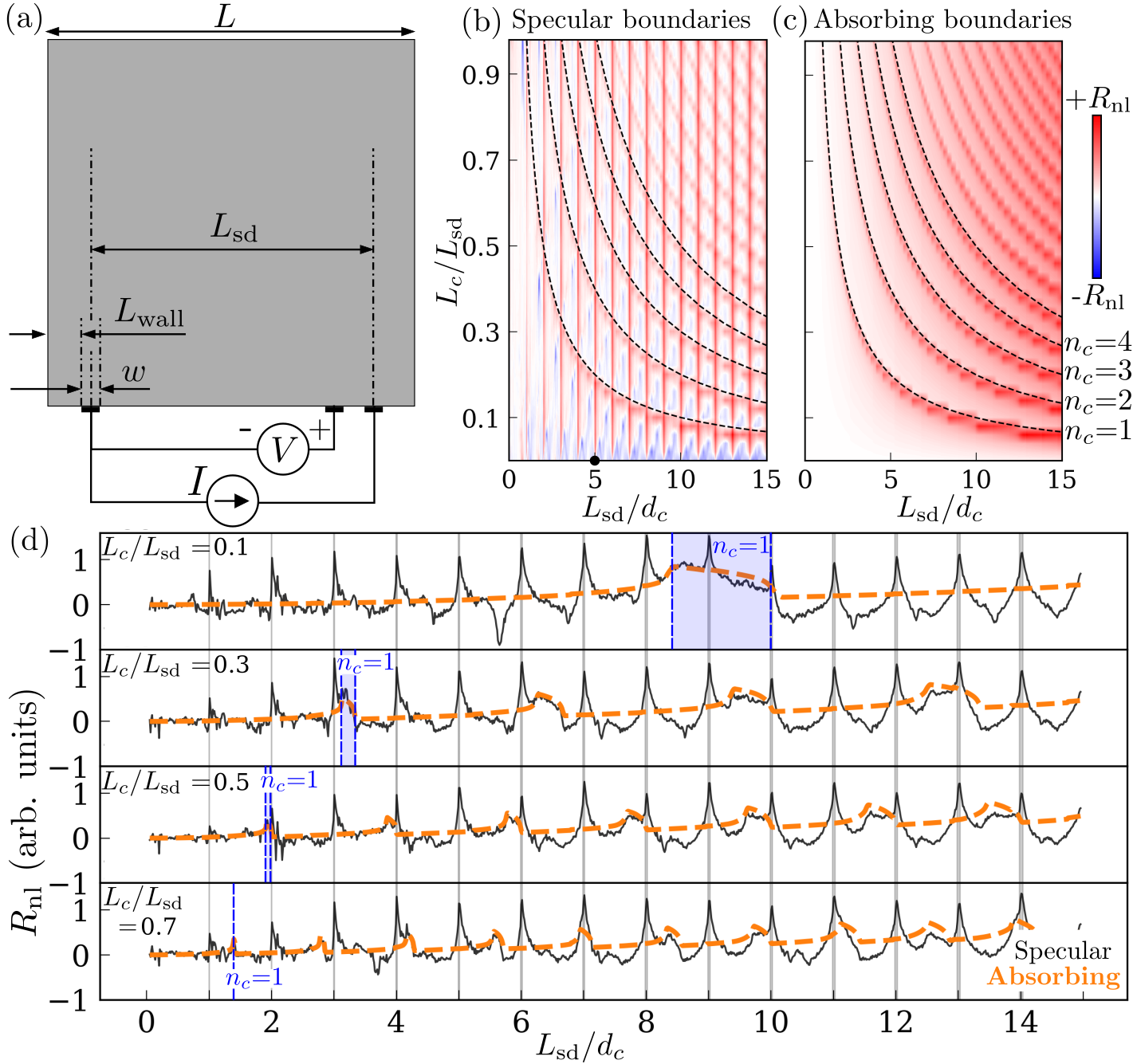
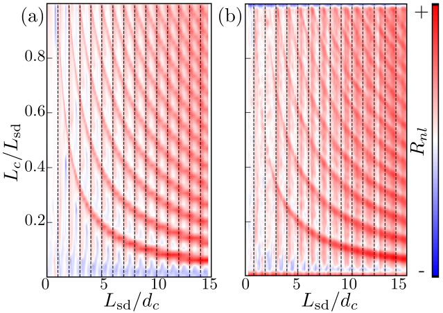
We perform simulations in a square domain of side (in arbitrary units), with varying PC widths (Appendix C), and for varying source and drain PC distances from the sidewalls (Appendix D), described by (device schematic in Fig. 2(a)). The simulations also consider specular as well as absorbing (non-specular) boundaries (Fig. 2). In the actual experiment’s device as mentioned we have and hence , and its boundaries are specular. In the simulations we consider the fiducial case of for all three PCs and , corresponding to source and drain PCs flush with the sidewalls and . Figure 2(b) shows a contour plot, simulated in the MC scheme, of where is constant while and are varied, for a device with specular boundaries, measured using a fictitious detector PC centered at . The intensity of red (blue) color in the contour plots indicate the magnitude of positive (negative) measured by the detector. The locations of the center of the source and drain PCs correspond to and (for which if ) on the vertical axis, respectively. The integer TMF peaks appear as hyperbolas obeying . The fractional peaks at integer appear as vertical features, independent of at every (see e. g. indicated by a black dot in Fig. 2(b)). When is computed for varying at a fixed , corresponding to a horizontal cut in the contour plot, the source-drain resonances appear as peaks at fractional . These peaks are depicted vs in Fig. 2(d), for better visualization of Fig. 2(b). By considering Figs. 2(a,b,d), we are able to explain features observed in the experimental data. First, the intersections of the vertical lines (due to source-drain resonances) with the hyperbolae of integer TMF peaks reveals why detector PCs closer to the source detect more fractional peaks. For a detector PC with , the fractional peaks occur at , yielding 9 fractional peaks below (including the one at , which lies within the shaded blue region in Fig. 2(d)). For a PC at , there are only 3 such peaks. Second, the values of at which the fractional peaks occur are indeed independent of , depending instead on the device-scale . As a result, the periodicity of the fractional peaks is also independent of , unlike the integer TMF peaks whose periodicity is . In Fig. 2(c), we consider the same device, but with the side and top boundaries absorbing rather than specular. The fractional peaks are now completely absent, with only the integer TMF peaks visible in . The absence of the fractional peaks signifies that device-scale specular boundary scattering is also necessary, unlike for integer TMF peaks which only require specular scattering off the bottom boundary.
In Fig. 2(b) where , the modeled oscillation amplitude of for the fractional peaks is larger than of the integer peaks, unlike the experimentally measured amplitude in Fig. 1(c-f). To explore the change, was modeled in the MC scheme for variable source and drain PC width in Appendix C. The model indicates that as is increased, the fractional peaks lose prominence and eventually the amplitudes of the integer peaks exceed those of the fractional peaks. The experimental findings in Fig. 1(c-f) hence are explained by relatively wider . The effects of larger source and drain PC distances from the sidewalls were also modeled in Appendix D. Increasing substantially diffuses the fractional peaks, contributing to the observations in Fig. 1(c-f). Hence narrow and small are beneficial for the fractional peaks to manifest. We have thus achieved a minimal model that reproduces the essential features of the experiment.
We performed a quantitative correlation between the experimental data and the model, via comparison of -values at which the fractional peaks occur in the experiment and the model. The model predicts a periodicity in given by , where . Analysis of the periodicity in in the data in Fig. 1(c-f) allows calculation of the device’s , in which any small systematic offsets in the experimental cancel out. This value of can be vetted against the lithographic length. Analysis of the data in Fig. 1(c-f) averaging over all PC combinations, yields m, in good agreement with the lithographic length m in Fig. 1(a).

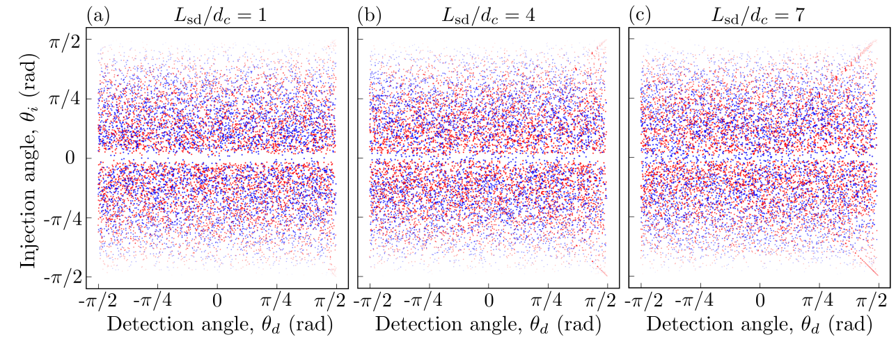
Individual single-particle trajectories can shed light on the unique origins of the fractional peaks, as illustrated in Fig. 3 where a square device of internal dimensions is modeled in the MC scheme. Figure 3 examines the trajectories that land in the detector PC, due to carriers originating from either the source (holes) or from the drain (electrons), using an approach labeled angle-resolved trajectory spectroscopy (ARTS, details in Appendix B). In Figs. 3(a,b,c,d) all PCs have , , while the source PC is centered at , and the drain PC centered at (, source and drain PCs flush with the sidewalls). The detector PC is centered at (hence ) for Fig. 3(a,b,c,e,f), while it is centered at () for Fig. 3(d,g,h). In Fig. 3(a), is chosen to correspond to the condition for observation of the integer TMF peak. Shown are a set of trajectories emanating from the source, with small injection angles centered around zero (tangents indicated by dashed red lines). These trajectories correspond to the usual single-particle intuition associated with the integer TMF peaks, with the spread in the injection angles due to the finite sizes of the source and detector PCs and the angular spread of trajectories due to the Fermi contour. Such trajectories are relatively insensitive to , robustly landing at the detector PC after following a direct cyclotron-orbit path from source PC to detector PC, conforming to TMF. The dashed black lines indicate tangents to the trajectories arriving over arrival angles at the detector PC, for (in rad). In Figs. 3(b-c), is chosen to correspond to the condition for observation of the fractional () peak. Figure 3(b) illustrates two trajectories arriving at the detector PC at very nearly identical (tangent indicated by dashed black line), but having traversed very different trajectories through the device: the red trajectory follows a hole injected from the source PC (at indicated by dashed red line), the blue trajectory follows an electron injected from the drain PC (at different indicated by dashed blue line). Yet Fig. 3(c) reveals that also trajectories exist which arrive at the detector PC over a small range of (tangents indicated by single dashed black line and values of indicated in the figure), but originate from still closely bunched non-diverging trajectories (red trajectories following holes injected from the source PC, values indicated by single dashed red line). Figure 3(d) shows trajectories at corresponding to the integer TMF peak, but now for a different detector location, . The figure shows that the span of for which injected trajectories reach the detector decreases as the detector PC is moved further away from the source PC.
The ARTS plots in Figs. 3(e-h) show the injection angle at source (hole trajectories, coded in red) or drain (electron trajectories, coded in blue) PCs vs the arrival angle at the detector PC. The opacity of the dots is weighted by , reflecting the injection distribution over in the MC scheme (fewer trajectories injected at high also mean fewer detected at the detector PC). Figure 3(e) corresponds to Fig. 3(a), with conforming to the condition for observing the integer TMF peak, while Fig. 3(f) corresponds to Figs. 3(b-c), with conforming to the condition for observing the fractional () peak. In Fig. 3(e) the contiguous-dot structure observed for indicates the integer TMF peak, and is attributed to the trajectories depicted in Fig. 3(a): over a small range of trajectories reliably land at the detector PC in a one-to-one relation to . The width of the contiguous-dot structure is proportional to . Less apparent contiguous-dot structures also exist in Fig. 3(e) for , corresponding to trajectories originating from the source or drain PCs and reaching the detector PC with more than one specular scattering event off the boundaries. Notably, between the contiguous regions in Fig. 3(e) exists a highly unordered pointillistic structure with a mix of electron and hole trajectories. The spatial profiles of trajectories in the unordered regions reveal that such trajectories that land on the detector PC at infinitesimally close can have uncorrelated , reflecting similar observations in Fig. 3(b). The contiguous-dot structure at originating in the integer TMF peak provides the dominant contribution to at the detector PC. The unordered regions do not cooperate to contribute a sizable signal. In Fig. 3(f) the horizontal blurred gap over all for correlates with the fractional () peak (explored for other in Appendix F). Example trajectories are shown in Figs. 3(b-c). The ARTS structure remains overall unordered, without noticeable contiguous-dot patterns, indicating mostly divergent trajectories. Hence, apart from the gap, strikingly ARTS reveals an absence of any contiguous structure to which the fractional peak can be attributed, unlike in the case of the integer TMF peak. The gap indicates a dearth of trajectories reaching the detector PC. This dearth is more acutely sensed in transport because the number of injected trajectories is weighted by , maximal for , congruent with the appearance of a fractional peak in measurements and modeling. We next consider a different detector location, . In Fig. 3(g), we set , conforming to the condition for observing the integer TMF peak. We again observe the contiguous-dot structure arising from trajectories near landing directly at the detector PC as expected at the integer TMF peak. Comparison with Fig. 3(e) shows that the width of the contiguous-dot structure is inversely related to , meaning that trajectories within a tighter span of reach the detector, consistent with Fig. 3(d). In Fig. 3(h) we consider the condition for the fractional peak again, but for . The blurred gap near is again observed, indicating a dearth of trajectories reaching the detector PC. The ARTS structure overall appears strikingly similar to Fig. 3(f), hinting that the phenomenology of fractional peaks is independent of the detector PC location. We infer that the source-drain resonance results in an increased number of hole (electron) trajectories finding an expeditious path from source (drain) PC to drain (source) PC, rapidly exiting the device and never arriving at the detector PC irrespective of its location. While the ARTS gap is striking, the exact mechanism of its relation to the formation of maxima in the nonlocal at the detector PC bears investigating in future work. Even the trajectories corresponding to the fewer dots within the blurred gap trace a complex trajectory through the device. The lack of dominant contribution from an ordered contiguous-dot structure (such as for TMF) precludes an intuitive explanation based on obvious single-particle trajectories. The fractional peaks in appear to build from many random events in the collective dynamics of the particle system. Fractional peaks hence require consideration of all trajectories and the collective dynamics of a particle distribution which includes electrons and holes. In contrast, the integer TMF peaks can be understood from more intuitive single-particle semiclassical ballistic cyclotron orbits with .
IV Correlation with backflow and vorticity
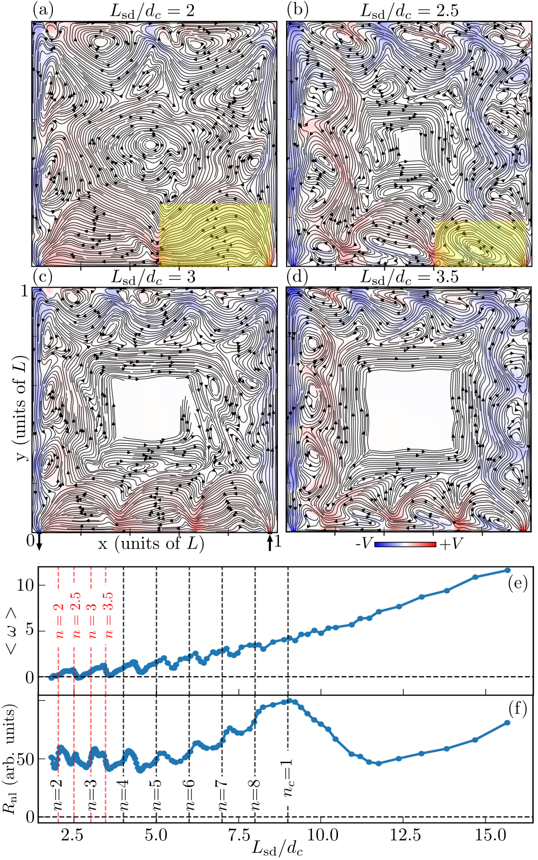
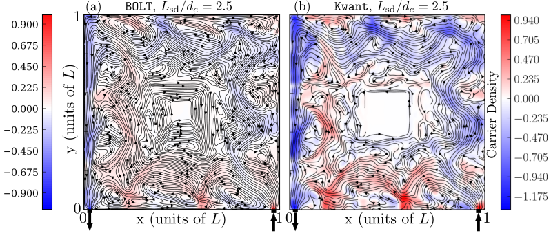
Another striking manifestation of the source-drain resonance condition is contained in Fig. 4, where we examine the relation between the spatial transport profile and the source-drain resonances. Figures 4(a-d) are obtained via the FV scheme and show current streamlines and color-coded voltage contour plots in the steady-state for an device with specular boundaries, with , and , at = 2, 2.5, 3 and 3.5 respectively. As mentioned previously, the ballistic regime can exhibit current vortices, characterized by a non-zero vorticity , where denotes the current density. The vector sum of many individual electron and hole trajectories over time gives rise to in the steady-state, which is hence the outcome of collective dynamics more intricate than understood from single-particle cyclotron orbits. Figure 4(a) examines the profiles for the fractional peak, at . A focusing of current streamlines occurs at the center of the bottom edge, with the conventional current flow from the source indicated by arrows. In keeping with the previously used color scheme, a red shading indicates a local overdensity of holes and a positive voltage, while blue shading indicates a local overdensity of electrons and a negative voltage. Fig. 4(a) shows an overdensity of holes and a positive voltage everywhere throughout the bottom edge. This overdensity of holes and positive voltage correspond to the fractional peak, as expected since fractional peaks occur independent of detector location . The associated current flow is unidirectional from source to the drain along the bottom edge. Figure 4(b) examines the profiles at . The focusing of current streamlines occurs where expected at the bottom edge but the overdensity of holes is around the center of the semiclassical cyclotron orbits (e.g. between the source and the first focusing location) now replaced with an overdensity of electrons and a locally negative voltage. The electrons originate from the drain and traverse the left, top and right boundaries. The overdensity of electrons and negative voltage result in a local backflow of the current, resulting in a striking phenomenon: the appearance of current vortices. Figures 4(c,d) repeat and confirm the phenomena, for the fractional peak and for the half-integer condition. At integer , corresponding to a fractional peak, the voltage along the bottom edge does not alternate sign (Figs. 4(a,c)), while at half-integer the voltage along the bottom edge alternates sign, causing backflow and current vortices (Figs. 4(b,d)).
Figures 4(e,f) are also obtained via the FV scheme. Figure 4(e) considers the vorticity averaged over an area /2, corresponding to a box covering one cyclotron orbit with its right-bottom corner located at the midpoint of the source PC (indicated by shaded yellow region in Figs. 4(a,b)), and shows the area-averaged vorticity vs . Remarkably, Fig. 4(e) shows that periodic features appear in vs and that peaks for half-integer . The spatial profiles of in also reveal the presence of current vortices along the bottom edge around half-integer values of (Figs. 4(b,d)) and the absence of vortices at integer values of (Figs. 4(a,c)). As noted, the absence of at integer corresponds to the existence of positive voltages throughout the bottom edge, in turn corresponding to the fractional peak in independent of . At half-integer locally negative voltages along the bottom edge cause the current backflow required for . In Fig. 4(f), is plotted vs for an arbitrarily chosen . In Fig. 4(e) the periodicity in is found to be , equalling the periodicity expected for the fractional peaks in . This indicates a strong correlation between (a property of the bulk of the device, not directly visualized experimentally) and (a property measured at the device boundary). At present a complete physical insight for the correlation between and is beyond the scope of this work. However the correlation underlines the importance of collective dynamics in ballistic transport, and highlights a complexity reaching beyond single-particle trajectories.
V Implications and conclusions
The experimental measurements and simulations both point to the existence of hitherto unsuspected structure in the nonlocal ballistic magnetoresistance in a square mesoscopic geometry with source, drain and voltage detection PCs, similar to the TMF measurement geometry. vs , recorded at the detector PC, shows a periodic structure at low , with peaks at locations where obeys , where . Since , the peaks occur at fractional , unlike the TMF peaks that occur at integer . The fractional peaks occur at source-drain resonances where in a semiclassical cyclotron orbit framework, injected carriers from the source PC would impinge directly on the drain PC after specular reflections off the device boundary. However unlike TMF peaks, fractional peaks cannot be explained by single-particle ballistic trajectories. The particle trajectories leading to the fractional peaks are complex, and no single dominant contribution from a coordinated ordered group of trajectories is identifiable. The lack of dominant coordinated trajectory contribution forestalls an explanation based on conspicuous single-particle trajectories. Instead, the fractional peaks in vs originate in the collective dynamics of the fermionic particle distribution, including electrons and holes, and require analysis and averaging of all trajectories.
Further the source-drain resonances and fractional peaks (boundary properties) are anticorrelated with vorticity in the current density streamlines, a bulk property and quintessentially a collective flow phenomenon. The current density itself results from the time-averaged collective sum of many individual electron and hole trajectories. The amplitude of the fractional peaks is sensitive to the locations of source and drain PCs and to PC conducting widths, but not to the location of the detector PC. The insensitivity to the location of the detector PC is related to the disappearance of vorticity along the bottom boundary at the condition of the fractional peaks.
The notable match between experiments and simulations supports the physical understanding that has been gained. The simulations can hence lead to new experimentally verifiable phenomena in ballistic transport in 2DESs and 2D hole systems or in recent materials with long carrier mean-free paths. The combined experiments and simulations can in future work also shed light on less understood and experimentally less-accessible aspects of low-dimensional transport, particularly vorticity. A main outcome of the work lies in the realization that ballistic transport results from a collective dynamics of a particle distribution and supports phenomena substantially more elaborate than those ostensibly deduced from single-particle cyclotron orbits.
Acknowledgements
The authors acknowledge computational resources (GPU cluster infer) and technical support provided by Advanced Research Computing at Virginia Tech and the Center for Computational Innovations at Rensselaer Polytechnic Institute. MJM acknowledges support from the U.S. Department of Energy, Office of Science, Office of Basic Energy Sciences, under award number DE-SC0020138. MC and RS acknowledge support from the National Science Foundation under grant No. DMR-1956015.
VI Appendices
VI.1 Appendix A: Experimental methods
The device is fabricated from a high- GaAs/AlGaAs heterostructure epitaxially grown using optimized molecular beam epitaxy. The 2DES resides in the GaAs quantum well, with depth (from the surface) of 190 nm and width 26 nm. The heterostructure uses a stepped barrier with Al alloy fractions 23% and 32% and is top- (9 1011 cm-2) and bottom-doped (4 1011 cm-2) using Si layers in Al0.32Ga0.68As with a setback of 80 nm. The growth and optimization of similar heterostructures is discussed in Ref. [63]. Samples in the van der Pauw configuration provide the transport parameters of the material under the same conditions as the device measurements, as listed in Table 1. The transport parameters are derived from sheet resistance and Hall measurements accounting for conduction band non-parabolicity with a -point effective mass where denotes the free electron mass. In particular, m is much larger than the device size m, and hence transport through the device is in the ballistic regime.
| Sheet resistance | 2.74 |
| 2D electron density | 3.40 m-2 |
| Mobility | 670 m2/Vs |
| Fermi wavevector | 1.46 m-1 |
| Fermi wavelength | 43.0 nm |
| Fermi velocity | 2.46 m/s |
| Fermi energy | 11.9 meV |
| Mean-free path | 64.5 m |
For device fabrication, a Hall mesa is first patterned using photolithography followed by wet etching in H2SO4/H2O2/H2O solution. The active region of the sample containing the square mesoscopic device is patterned using electron beam lithography using PMMA as the etching mask, followed by gentle and shallower wet etching in the same solution, resulting in smooth device boundaries. The depletion layer (200 nm) forming between 2DES and etched boundaries smoothens out the potential over length scales smaller than the Fermi wavelength by exponentially attenuating the high spatial frequency components of the potential. This results in specular boundaries. N-type Ohmic contacts are annealed InSn. The device is measured in a cryostat at = 4.1 K after LED illumination and stabilization. All measurements are obtained using low-frequency lock-in techniques under low ac current excitation (100 nA to 200 nA). To experimentally detect and resolve the fractional peaks, very precise measurements of are needed, achieved using a gaussmeter and high-resolution stepping of the magnet current in each experimental run.
VI.2 Appendix B: Transport simulations
To simulate magnetotransport in the devices in the FV scheme BOLT [8] is used, a solver framework for the Boltzmann transport equation (Eq. 1). The modeling takes the band structure of the material and device geometry (spatial and momentum space shape) as input. A square device is considered, with spatial dimensions , discretized into 250 250 numerical zones. In momentum space, we take the zero-temperature limit and hence the carriers are confined to the nearly circular Fermi contour, which is discretized using 1024 numerical zones. This 1D momentum space allows the simulations to be sped up significantly. The model assumes that transport is collisionless (i.e., there are no momentum-relaxing or momentum-conserving electron-electron interactions), and the system is in the ideal ballistic regime. The device boundaries are assumed to be perfectly specular. Current injection (extraction) is achieved by imposing a shifted Fermi-Dirac distribution at the location of the source (drain) contacts. The device is initialized with a thermal distribution everywhere else, which is then evolved as a function of time until steady state is reached. Currents and voltages at any time instant can then be calculated from the carrier distribution function as described in [8].
In the MC scheme, holes (electrons) are injected through the source (drain) by randomly sampling the distribution with particles. The trajectory of each injected particle is evolved analytically by computing the intersections of the circular orbits with the device boundaries, until the particle exits through either the source or the drain. For the ARTS (angle-resolved trajectory spectroscopy) calculations, we discretize the arrival angle, , into equally-spaced angles, each of which generates a single trajectory. We then analytically integrate this trajectory (as in the MC scheme) backwards till it reaches the source or the drain. We note the final angle which the trajectory makes upon striking the source or drain, which we call the injection angle. Each point in the ARTS plots (Figs. 3(d,e)) corresponds to a single trajectory measured by the detector, with its size weighted by a factor. The uniform discretization in the ARTS scheme is essential for a key point: the random distribution of trajectories in the ARTS plots is not due to a random sampling of the trajectories, but rather due to a deterministic outcome obtained by analytically evolving trajectories that are equally spaced on the Fermi contour.
.
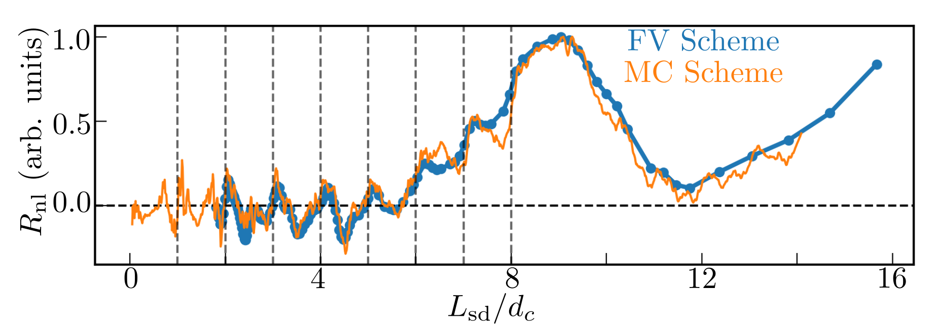
The MC and FV schemes solve the same semiclassical Boltzmann equation (Eq. 1), yet via different numerical schemes. The MC scheme analytically computes the intersections of individual carrier trajectories with the device boundaries, while the FV scheme evolves the carrier distribution over the entire device as a function of time. Each scheme has its own advantages - the MC scheme is inherently faster because calculations are performed only at device boundaries, while the FV scheme allows for visualization of properties in the bulk of the device (such as current vortices). Figure 5 compares (in arbitrary units) vs obtained using the two schemes at detector location in a square device of side , with , and . The results have been normalized to aid comparison, and indicate that both numerical schemes yield consistent results.
VI.3 Appendix C: Effect of source and drain PC width on fractional peaks
.
We observe that in the modeling in Fig. 2(b) with narrow , the modeled oscillation amplitude of for the fractional peaks is larger than for the integer peaks, while the experimentally measured amplitude in Fig. 1(c-f) (where ) shows the opposite trend. Hence, using the MC scheme we modeled for variable source and drain PC width , keeping . We use the same earlier square device, with dimensions in arbitrary units and specular boundaries. Results are depicted in Fig. 6, showing that an increase in results in a decrease in fractional peak amplitudes and in a small systematic shift of the peak to . As is increased, the fractional peaks lose prominence and eventually the amplitudes of the integer peaks surpass amplitudes of the fractional peaks. Moreover, for fractional peaks occur at exactly and are very sharp, much narrower than the integer TMF peaks, which are broadened by the angular spread of the injected carriers due to the existence of a Fermi contour.
VI.4 Appendix D: Effect of distance of source and drain PCs from side walls on fractional peaks
.
We identify the source and drain PC separation from the sidewalls as another factor that affects the amplitude of fractional peaks relative to that of the integer TMF peaks. In this section, we consider the evolution of when the source and drain PCs are situated at progressively larger distances from the sidewalls. Using the MC scheme we modeled for variable , keeping fixed . We use the same earlier square device, with dimensions in arbitrary units and specular boundaries. Results are depicted in Fig. 7. For larger , the fractional peaks are diffused and barely visible over the background in . Evidently small favors robust fractional peaks.
The effects of larger and are observed in the experimental results in Fig. 2(b) (where , ) and in the computational results in Fig. 4(f) (where , ). The fractional peak amplitudes are in these figures smaller than the integer TMF peak amplitudes (indicated by ), and the fractional peaks are shifted to .
VI.5 Appendix E: Quantum-coherent transport model
While fractional peaks appear in simulations based on the semiclassical Boltzmann equation (Eq. 1) solved in either the FV or MC scheme, we here ask what the effect is of quantum-coherent transport and how similar results are to semiclassical transport. The key differences when compared to the semiclassical model are the presence of quantum interference and a finite number of transverse modes injected through the PCs. To quantitatively address the comparison, we solve for ballistic quantum-coherent transport using the KWANT code [64], which solves the tight-binding model,
| (2) |
The above is obtained from a finite-difference approximation of the continuous Hamiltonian on a square lattice with spacing , and in the Landau gauge with vector potential . Here and we set . The dependence on enters through the non-dimensional parameter (ratio of the magnetic flux through one cell of the square lattice to the flux quantum ). The first term denotes the on-site energy, with a summation over all individual sites, and the second term a summation over nearest neighboring sites, with denoting the coordinate of the site (and similarly for ). The semiclassical model corresponds to the limit , whereas quantum-coherent transport has only been solved for in the few mode limit (e.g., [65, 66, 53]). To approach the semiclassical limit using a tight-binding model for the given geometry is challenging since we require and ; the first inequality corresponds to the ideal condition needed for the fractional peaks to manifest, and the second condition signifies . We thus consider a 50005000 site model with infinite leads placed on the bottom edge, each sites wide. We set , consistent with the requirement needed for a continuous approximation () and a nearly circular Fermi contour. With these parameters, we obtain 32 modes. We compute the carrier densities at site , and currents from site to site using,
| (3) | ||||
| (4) |
where denote the modes originating from a chosen lead (either source or drain). The index runs over all the modes up to energy in the lead and denotes the sites. is the hopping matrix element from site to , defined by , where is the Hamiltonian given in Eq. 2. The electron-hole symmetry at the Fermi surface allows for transport both by holes injected through the source PC and by electrons injected through the drain PC. Therefore, we need to compute scattering states originating from both the source and drain, and then evaluate the corresponding and for hole and electron modes respectively. The net carrier density is then , which is proportional to the voltage at site . The calculations for follow similarly.
Figure 8(a) shows the net carrier density ( voltage) at every lattice site obtained from KWANT for the fractional peak for a 50005000 site, with sites wide (corresponding to ), , , and with 32 hole modes injected through the source PC and 32 electron modes injected through the drain PC. In order to compare the voltages and currents obtained from the tight-binding KWANT model to the semiclassical model, the tight-binding solutions need to be appropriately averaged. Figure 8(b) shows the density (as shown in Fig. 8(a)) averaged over adjacent sites, corresponding to the low-energy limit of the lattice solution, which now resembles the semiclassical model.
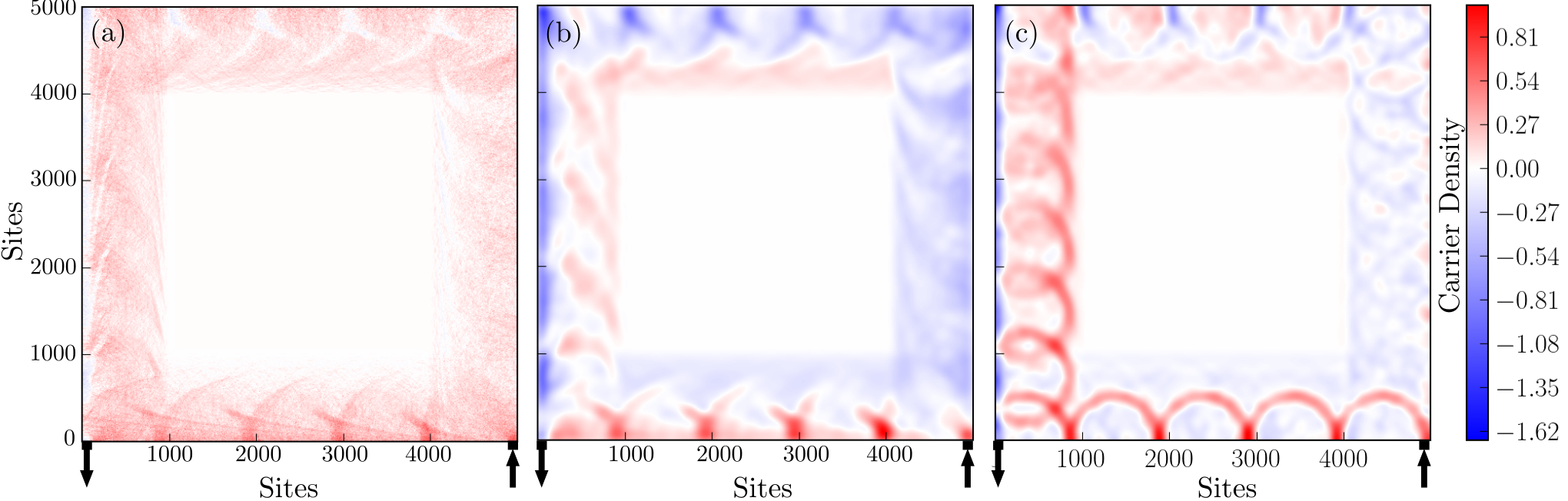
The question arises whether the fractional peaks also appear if just a few modes are considered or whether they require a summation of several modes. Figure 8(c) shows the voltage contour plot (averaged over adjacent sites) when only a single hole mode and a single electron mode are considered as compared to Fig. 8(b) where 32 modes of each are considered. In our color convention, the single-mode calculation shows alternating positive (red) and negative (blue) voltages at the bottom edge of the device, while in the multimode calculation, the voltage at the bottom edge remains positive (red) throughout. The results of the multimode calculation are consistent with the observation of the fractional peak - a hole overdensity everywhere on the bottom edge, while the single-mode calculation does not indicate this observation. Another noticeable effect in both voltage contour plots (but more so in the single-mode) is that the cyclotron orbits (red semicircular structures) do not impinge on the drain PC at exactly the fifth reflection from the boundary, instead appearing to land somewhat farther. This can be attributed to the effect of finite , with the number of reflections compounding the effect further (as observed in [2]). Finally, in the multimode calculation the intensity of red semicircular orbits decays as we move farther away from the source PC. The single-mode calculation, however, fails to capture this important effect. Figure 9 directly compares the densities and currents between KWANT and BOLT (FV scheme) at , in the same geometry as shown in Figs. 4(a-d) of the main text. The qualitative match is evident. Figure 10 compares the contour plots of vs and between the semiclassical transport model (using the MC scheme) and the quantum-coherent model for a square device with specular boundaries, length , , and . Fractional peaks are clearly evident in both the semiclassical and quantum-coherent transport models, with the location of peaks matching closely at lower values.
.
.
VI.6 Appendix F: ARTS plots at integer
.
As illustrated in Figs. 3(f,h) at the condition for appearance of fractional peaks, i.e. at integer , the ARTS plots show a characteristic horizontal gap around . This gap indicates a lack of trajectories that reach the detector PC. We show in Fig. 11 that this gap blurs with increasing . As increases, the trajectories traverse longer path lengths before reaching the source/drain, increasing their likelihood of being randomized. The randomization of the trajectories leads to an increased probability that they reach the detector PC, instead of the source/drain PCs. Note that, as mentioned in the main text, the randomization here is deterministic; each trajectory follows an analytic solution obtained by a specular reflection off the device boundaries.
References
- Gupta et al. [2021a] A. Gupta, J. J. Heremans, G. Kataria, M. Chandra, S. Fallahi, G. C. Gardner, and M. J. Manfra, Hydrodynamic and ballistic transport over large length scales in , Phys. Rev. Lett. 126, 076803 (2021a).
- Gupta et al. [2021b] A. Gupta, J. J. Heremans, G. Kataria, M. Chandra, S. Fallahi, G. C. Gardner, and M. J. Manfra, Precision measurement of electron-electron scattering in GaAs/AlGaAs using transverse magnetic focusing, Nat. Commun. 12, 5048 (2021b).
- Spector et al. [1990] J. Spector, H. Stormer, K. Baldwin, L. Pfeiffer, and K. West, Ballistic electron transport beyond 100 microm in 2D electron systems, Surf. Sci. 228, 283 (1990).
- Chen et al. [2004] H. Chen, J. J. Heremans, J. A. Peters, N. Goel, S. J. Chung, and M. B. Santos, Ballistic transport in InSb/InAlSb antidot lattices, Appl. Phys. Lett. 84, 5380 (2004).
- Gilbertson et al. [2011] A. M. Gilbertson, A. Kormányos, P. D. Buckle, M. Fearn, T. Ashley, C. J. Lambert, S. A. Solin, and L. F. Cohen, Room temperature ballistic transport in InSb quantum well nanodevices, Appl. Phys. Lett. 99, 242101 (2011).
- Lee et al. [2016] M. Lee, J. R. Wallbank, P. Gallagher, K. Watanabe, T. Taniguchi, V. I. Fal’ko, and D. Goldhaber-Gordon, Ballistic miniband conduction in a graphene superlattice, Science 353, 1526 (2016).
- Banszerus et al. [2016] L. Banszerus, M. Schmitz, S. Engels, M. Goldsche, K. Watanabe, T. Taniguchi, B. Beschoten, and C. Stampfer, Ballistic transport exceeding 28 m in CVD grown graphene, Nano Lett. 16, 1387 (2016).
- Chandra et al. [2019a] M. Chandra, G. Kataria, D. Sahdev, and R. Sundararaman, Hydrodynamic and ballistic AC transport in two-dimensional fermi liquids, Phys. Rev. B 99, 165409 (2019a).
- Chandra et al. [2019b] M. Chandra, G. Kataria, and D. Sahdev, Quantum critical ballistic transport in two-dimensional fermi liquids, arXiv:1910.13737 (2019b).
- Shytov et al. [2018] A. Shytov, J. F. Kong, G. Falkovich, and L. Levitov, Particle collisions and negative nonlocal response of ballistic electrons, Phys. Rev. Lett. 121, 176805 (2018).
- Bandurin et al. [2018] D. A. Bandurin, A. V. Shytov, L. S. Levitov, R. K. Kumar, A. I. Berdyugin, M. Ben Shalom, I. V. Grigorieva, A. K. Geim, and G. Falkovich, Fluidity onset in graphene, Nat. Commun. 9, 4533 (2018).
- Nazaryan and Levitov [2021] K. G. Nazaryan and L. Levitov, Robustness of vorticity in electron fluids, arXiv:2111.09878 (2021).
- van Houten et al. [1989] H. van Houten, C. W. J. Beenakker, J. G. Williamson, M. E. I. Broekaart, P. H. M. van Loosdrecht, B. J. van Wees, J. E. Mooij, C. T. Foxon, and J. J. Harris, Coherent electron focusing with quantum point contacts in a two-dimensional electron gas, Phys. Rev. B 39, 8556 (1989).
- Molenkamp and de Jong [1994] L. W. Molenkamp and M. J. M. de Jong, Electron-electron-scattering-induced size effects in a two-dimensional wire, Phys. Rev. B 49, 5038 (1994).
- de Jong and Molenkamp [1995] M. J. M. de Jong and L. W. Molenkamp, Hydrodynamic electron flow in high-mobility wires, Phys. Rev. B 51, 13389 (1995).
- Heremans et al. [1992] J. J. Heremans, M. B. Santos, and M. Shayegan, Observation of magnetic focusing in two‐dimensional hole systems, Appl. Phys. Lett. 61, 1652 (1992).
- Heremans et al. [1999] J. J. Heremans, S. von Molnár, D. D. Awschalom, and A. C. Gossard, Ballistic electron focusing by elliptic reflecting barriers, Appl. Phys. Lett. 74, 1281 (1999).
- Chen et al. [2005] H. Chen, J. J. Heremans, J. A. Peters, A. O. Govorov, N. Goel, S. J. Chung, and M. B. Santos, Spin-polarized reflection in a two-dimensional electron system, Appl. Phys. Lett. 86, 032113 (2005).
- Govorov and Heremans [2004] A. O. Govorov and J. J. Heremans, Hydrodynamic effects in interacting fermi electron jets, Phys. Rev. Lett. 92, 026803 (2004).
- Keser et al. [2021] A. C. Keser, D. Q. Wang, O. Klochan, D. Y. H. Ho, O. A. Tkachenko, V. A. Tkachenko, D. Culcer, S. Adam, I. Farrer, D. A. Ritchie, O. P. Sushkov, and A. R. Hamilton, Geometric control of universal hydrodynamic flow in a two-dimensional electron fluid, Phys. Rev. X 11, 031030 (2021).
- Levin et al. [2018] A. D. Levin, G. M. Gusev, E. V. Levinson, Z. D. Kvon, and A. K. Bakarov, Vorticity-induced negative nonlocal resistance in a viscous two-dimensional electron system, Phys. Rev. B 97, 245308 (2018).
- Gusev et al. [2018] G. M. Gusev, A. D. Levin, E. V. Levinson, and A. K. Bakarov, Viscous electron flow in mesoscopic two-dimensional electron gas, AIP Adv. 8, 025318 (2018).
- Braem et al. [2018] B. A. Braem, F. M. D. Pellegrino, A. Principi, M. Röösli, C. Gold, S. Hennel, J. V. Koski, M. Berl, W. Dietsche, W. Wegscheider, M. Polini, T. Ihn, and K. Ensslin, Scanning gate microscopy in a viscous electron fluid, Phys. Rev. B 98, 241304 (2018).
- Auton et al. [2016] G. Auton, J. Zhang, R. K. Kumar, H. Wang, X. Zhang, Q. Wang, E. Hill, and A. Song, Graphene ballistic nano-rectifier with very high responsivity, Nat. Commun. 7, 11670 (2016).
- Taychatanapat et al. [2013] T. Taychatanapat, K. Watanabe, T. Taniguchi, and P. Jarillo-Herrero, Electrically tunable transverse magnetic focusing in graphene, Nat. Phys. 9, 225 (2013).
- Mayorov et al. [2011] A. S. Mayorov, R. V. Gorbachev, S. V. Morozov, L. Britnell, R. Jalil, L. A. Ponomarenko, P. Blake, K. S. Novoselov, K. Watanabe, T. Taniguchi, and A. K. Geim, Micrometer-scale ballistic transport in encapsulated graphene at room temperature, Nano Lett. 11, 2396 (2011).
- Lucas and Fong [2018] A. Lucas and K. C. Fong, Hydrodynamics of electrons in graphene, J. Phys.: Condens. Matter 30, 053001 (2018).
- Sulpizio et al. [2019] J. A. Sulpizio, L. Ella, A. Rozen, J. Birkbeck, D. J. Perello, D. Dutta, M. Ben-Shalom, T. Taniguchi, K. Watanabe, T. Holder, R. Queiroz, A. Principi, A. Stern, T. Scaffidi, A. K. Geim, and S. Ilani, Visualizing poiseuille flow of hydrodynamic electrons, Nature 576, 75 (2019).
- Pezzini et al. [2020] S. Pezzini, V. Mišeikis, S. Pace, F. Rossella, K. Watanabe, T. Taniguchi, and C. Coletti, High-quality electrical transport using scalable CVD graphene, 2D Mater. 7, 041003 (2020).
- Krishna Kumar et al. [2017] R. Krishna Kumar, D. A. Bandurin, F. M. D. Pellegrino, Y. Cao, A. Principi, H. Guo, G. H. Auton, M. Ben Shalom, L. A. Ponomarenko, G. Falkovich, K. Watanabe, T. Taniguchi, I. V. Grigorieva, L. S. Levitov, M. Polini, and A. K. Geim, Superballistic flow of viscous electron fluid through graphene constrictions, Nat. Phys. 13, 1182 (2017).
- Bandurin et al. [2016] D. A. Bandurin, I. Torre, R. K. Kumar, M. B. Shalom, A. Tomadin, A. Principi, G. H. Auton, E. Khestanova, K. S. Novoselov, I. V. Grigorieva, L. A. Ponomarenko, A. K. Geim, and M. Polini, Negative local resistance caused by viscous electron backflow in graphene, Science 351, 1055 (2016).
- Berdyugin et al. [2020] A. I. Berdyugin, B. Tsim, P. Kumaravadivel, S. G. Xu, A. Ceferino, A. Knothe, R. K. Kumar, T. Taniguchi, K. Watanabe, A. K. Geim, I. V. Grigorieva, and V. I. Fal’ko, Minibands in twisted bilayer graphene probed by magnetic focusing, Science Adv. 6, eaay7838 (2020).
- Jenkins et al. [2022] A. Jenkins, S. Baumann, H. Zhou, S. A. Meynell, Y. Daipeng, K. Watanabe, T. Taniguchi, A. Lucas, A. F. Young, and A. C. Bleszynski Jayich, Imaging the breakdown of ohmic transport in graphene, Phys. Rev. Lett. 129, 087701 (2022).
- Fei et al. [2017] Z. Fei, T. Palomaki, S. Wu, W. Zhao, X. Cai, B. Sun, P. Nguyen, J. Finney, X. Xu, and D. H. Cobden, Edge conduction in monolayer WTe2, Nat. Phys. 13, 677 (2017).
- Vool et al. [2021] U. Vool, A. Hamo, G. Varnavides, Y. Wang, T. X. Zhou, N. Kumar, Y. Dovzhenko, Z. Qiu, C. A. C. Garcia, A. T. Pierce, J. Gooth, P. Anikeeva, C. Felser, P. Narang, and A. Yacoby, Imaging phonon-mediated hydrodynamic flow in WTe2, Nat. Phys. 17, 1216 (2021).
- Zhu et al. [2015] Z. Zhu, X. Lin, J. Liu, B. Fauqué, Q. Tao, C. Yang, Y. Shi, and K. Behnia, Quantum oscillations, thermoelectric coefficients, and the fermi surface of semimetallic , Phys. Rev. Lett. 114, 176601 (2015).
- Aharon-Steinberg et al. [2022] A. Aharon-Steinberg, T. Völkl, A. Kaplan, A. K. Pariari, I. Roy, T. Holder, Y. Wolf, A. Y. Meltzer, Y. Myasoedov, M. E. Huber, B. Yan, G. Falkovich, L. S. Levitov, M. Hücker, and E. Zeldov, Direct observation of vortices in an electron fluid, arXiv:2202.02798 (2022).
- Hicks et al. [2012] C. W. Hicks, A. S. Gibbs, A. P. Mackenzie, H. Takatsu, Y. Maeno, and E. A. Yelland, Quantum oscillations and high carrier mobility in the delafossite , Phys. Rev. Lett. 109, 116401 (2012).
- Bachmann et al. [2019] M. D. Bachmann, A. L. Sharpe, A. W. Barnard, C. Putzke, M. König, S. Khim, D. Goldhaber-Gordon, A. P. Mackenzie, and P. J. W. Moll, Super-geometric electron focusing on the hexagonal fermi surface of PdCoO2, Nat. Commun. 10, 5081 (2019).
- Putzke et al. [2020] C. Putzke, M. D. Bachmann, P. McGuinness, E. Zhakina, V. Sunko, M. Konczykowski, T. Oka, R. Moessner, A. Stern, M. König, S. Khim, A. P. Mackenzie, and P. J. Moll, h/e oscillations in interlayer transport of delafossites, Science 368, 1234 (2020).
- Bachmann et al. [2022] M. D. Bachmann, A. L. Sharpe, G. Baker, A. W. Barnard, C. Putzke, T. Scaffidi, N. Nandi, P. H. McGuinness, E. Zhakina, M. Moravec, S. Khim, M. König, D. Goldhaber-Gordon, D. A. Bonn, A. P. Mackenzie, and P. J. W. Moll, Directional ballistic transport in the two-dimensional metal PdCoO2, Nat. Phys. 10.1038/s41567-022-01570-7 (2022).
- Moll et al. [2016] P. J. W. Moll, P. Kushwaha, N. Nandi, B. Schmidt, and A. P. Mackenzie, Evidence for hydrodynamic electron flow in PdCoO2, Science 351, 1061 (2016).
- Nandi et al. [2018] N. Nandi, T. Scaffidi, P. Kushwaha, S. Khim, M. E. Barber, V. Sunko, F. Mazzola, P. D. C. King, H. Rosner, P. J. W. Moll, M. König, J. E. Moore, S. Hartnoll, and A. P. Mackenzie, Unconventional magneto-transport in ultrapure PdCoO2 and PtCoO2, npj Quantum Mater. 3, 66 (2018).
- Harada [2021] T. Harada, Thin-film growth and application prospects of metallic delafossites, Mater. Today Adv. 11, 100146 (2021).
- Mackenzie [2017] A. P. Mackenzie, The properties of ultrapure delafossite metals, Rep. Prog. Phys. 80, 032501 (2017).
- Danz and Narozhny [2020] S. Danz and B. N. Narozhny, Vorticity of viscous electronic flow in graphene, 2D Mater. 7, 035001 (2020).
- Kaushal et al. [2011] V. Kaushal, I. I. de-la Torre, and M. Margala, Nonlinear electron properties of an InGaAs/InAlAs-based ballistic deflection transistor: Room temperature dc experiments and numerical simulations, Solid-State Electron. 56, 120 (2011).
- Chatzikyriakou et al. [2022] E. Chatzikyriakou, J. Wang, L. Mazzella, A. Lacerda-Santos, M. C. d. S. Figueira, A. Trellakis, S. Birner, T. Grange, C. Bäuerle, and X. Waintal, Unveiling the charge distribution of a GaAs-based nanoelectronic device: A large experimental dataset approach, Phys. Rev. Research 4, 043163 (2022).
- Percebois and Weinmann [2021] G. J. Percebois and D. Weinmann, Deep neural networks for inverse problems in mesoscopic physics: Characterization of the disorder configuration from quantum transport properties, Phys. Rev. B 104, 075422 (2021).
- Toussaint et al. [2018] S. Toussaint, F. Martins, S. Faniel, M. G. Pala, L. Desplanque, X. Wallart, H. Sellier, S. Huant, V. Bayot, and B. Hackens, On the origins of transport inefficiencies in mesoscopic networks, Scientific Rep. 8, 3017 (2018).
- Tsoi [1974] V. S. Tsoi, Focusing of electrons in a metal by a transverse magnetic field, JETP Lett. 19, 70 (1974).
- Tsoi et al. [1999] V. S. Tsoi, J. Bass, and P. Wyder, Studying conduction-electron/interface interactions using transverse electron focusing, Rev. Mod. Phys. 71, 1641 (1999).
- Lee et al. [2022] Y. K. Lee, J. S. Smith, and J. H. Cole, Influence of device geometry and imperfections on the interpretation of transverse magnetic focusing experiments, Nanoscale Res. Lett. 17, 31 (2022).
- Tsoǐ [1975] V. S. Tsoǐ, Determination of the dimensions of nonextremal Fermi-surface sections by transverse focusing of electrons, JETP Lett. 22, 197 (1975).
- Goldman et al. [1994] V. J. Goldman, B. Su, and J. K. Jain, Detection of composite fermions by magnetic focusing, Phys. Rev. Lett. 72, 2065 (1994).
- Smet et al. [1996] J. H. Smet, D. Weiss, R. H. Blick, G. Lütjering, K. von Klitzing, R. Fleischmann, R. Ketzmerick, T. Geisel, and G. Weimann, Magnetic focusing of composite fermions through arrays of cavities, Phys. Rev. Lett. 77, 2272 (1996).
- Heremans et al. [2007] J. J. Heremans, H. Chen, M. B. Santos, N. Goel, W. Van Roy, and G. Borghs, Spin‐dependent transverse magnetic focusing in InSb‐ and InAs‐based heterostructures, AIP Conf. Proc. 893, 1287 (2007).
- Rendell et al. [2022] M. J. Rendell, S. D. Liles, A. Srinivasan, O. Klochan, I. Farrer, D. A. Ritchie, and A. R. Hamilton, Gate voltage dependent rashba spin splitting in hole transverse magnetic focusing, Phys. Rev. B 105, 245305 (2022).
- Taubert et al. [2011a] D. Taubert, G. J. Schinner, C. Tomaras, H. P. Tranitz, W. Wegscheider, and S. Ludwig, An electron jet pump: The venturi effect of a fermi liquid, J. Appl. Phys. 109, 102412 (2011a).
- Taubert et al. [2010] D. Taubert, G. J. Schinner, H. P. Tranitz, W. Wegscheider, C. Tomaras, S. Kehrein, and S. Ludwig, Electron-avalanche amplifier based on the electronic venturi effect, Phys. Rev. B 82, 161416 (2010).
- Firdaus et al. [2018] H. Firdaus, T. Watanabe, M. Hori, D. Moraru, Y. Takahashi, A. Fujiwara, and Y. Ono, Electron aspirator using electron–electron scattering in nanoscale silicon, Nat. Commun. 9, 4813 (2018).
- Taubert et al. [2011b] D. Taubert, C. Tomaras, G. J. Schinner, H. P. Tranitz, W. Wegscheider, S. Kehrein, and S. Ludwig, Relaxation of hot electrons in a degenerate two-dimensional electron system: Transition to one-dimensional scattering, Phys. Rev. B 83, 235404 (2011b).
- Gardner et al. [2016] G. C. Gardner, S. Fallahi, J. D. Watson, and M. J. Manfra, Modified MBE hardware and techniques and role of gallium purity for attainment of two dimensional electron gas mobility 35×106 cm2/vs in AlGaAs/GaAs quantum wells grown by MBE, J. Cryst. Growth 441, 71 (2016).
- Groth et al. [2014] C. W. Groth, M. Wimmer, A. R. Akhmerov, and X. Waintal, Kwant: a software package for quantum transport, New Journal of Phys. 16, 063065 (2014).
- Stegmann et al. [2013] T. Stegmann, D. E. Wolf, and A. Lorke, Magnetotransport along a boundary: from coherent electron focusing to edge channel transport, New Journal of Phys. 15, 113047 (2013).
- LaGasse and Lee [2017] S. W. LaGasse and J. U. Lee, Understanding magnetic focusing in graphene junctions through quantum modeling, Phys. Rev. B 95, 155433 (2017).