[b]Regina Caputo
AstroPix: CMOS pixels in space
Abstract
Space-based gamma-ray telescopes such as the Fermi Large Area Telescope have used single sided silicon strip detectors to measure the position of charged particles produced by incident gamma rays with high resolution. At energies in the Compton regime and below, two dimensional position information within a single detector is required. Double sided silicon strip detectors are one option; however, this technology is difficult to fabricate and large arrays are susceptible to noise. This work outlines the development and implementation of monolithic CMOS active pixel silicon sensors, AstroPix, for use in future gamma-ray telescopes. Based upon detectors designed using the HVCMOS process at the Karlsruhe Institute of Technology, AstroPix has the potential to maintain the high energy and angular resolution required of a medium-energy gamma-ray telescope while reducing noise with the dual detection-and-readout capabilities of a CMOS chip. The status of AstroPix development and testing as well as outlook for application in future telescopes is presented.
1 Motivation and Previous Work
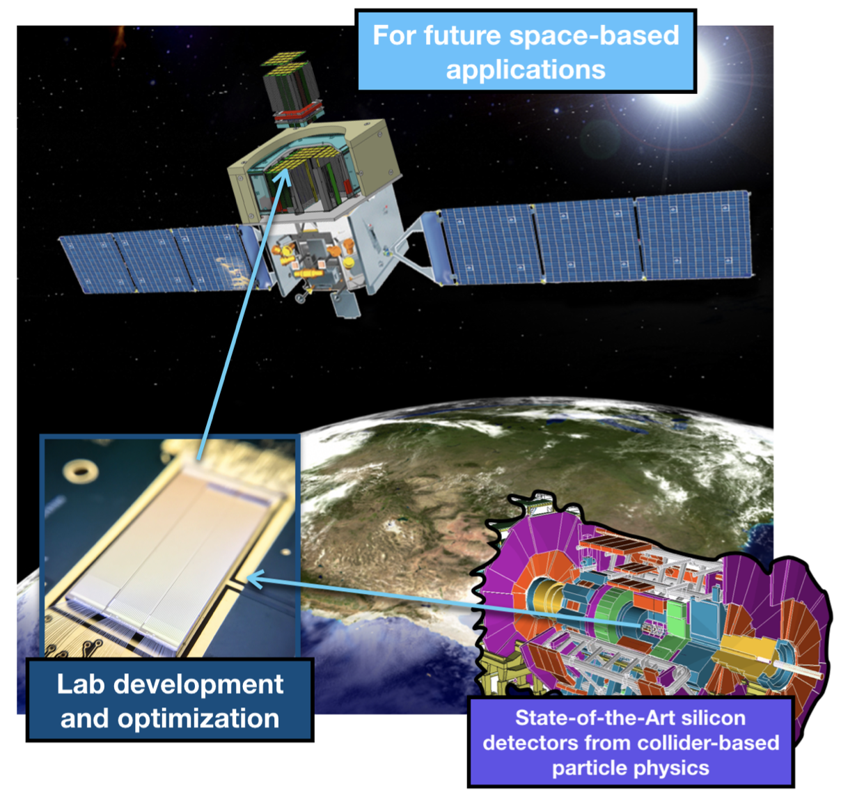
The AstroPix project aims to develop and test pixelated silicon sensors for use in space-based gamma-ray instruments. This novel space-based technology is based upon work done with similar detectors at the Large Hadron Collider [8], and could contribute to a host of future instruments such as a next-generation wide-field gamma-ray explorer whose time domain capabilities is prioritized in the Astro2020 Decadal Survey [6]. This work will overview the design, testing, and development of AstroPix version 2. This version is a step toward a flight prototype which will be realized with version 3 (Section 3). The long-term goal is to continue this development and testing in order to determine AstroPix performance and its suitability for use in space (Fig. 1).
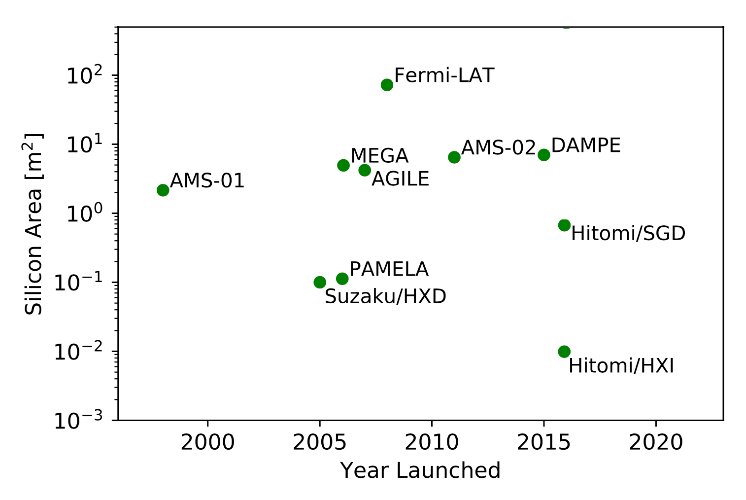
Heritage technology used for tracking instruments on previous gamma-ray, hard X-ray, and cosmic ray instruments include single-sided silicon strip detectors, double-sided silicon strip detectors (Fig. 2), and other pixelated detectors. Each design carries unique strengths and weaknesses regarding event timing, position resolution, readout efficiency, noise, energy resolution, and power consumption. The evolution of silicon tracker technology used in for the study of astrophysics in space has been made possible in part through its long history of implementing technologies developed by ground-based particle physics experiments.
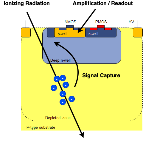
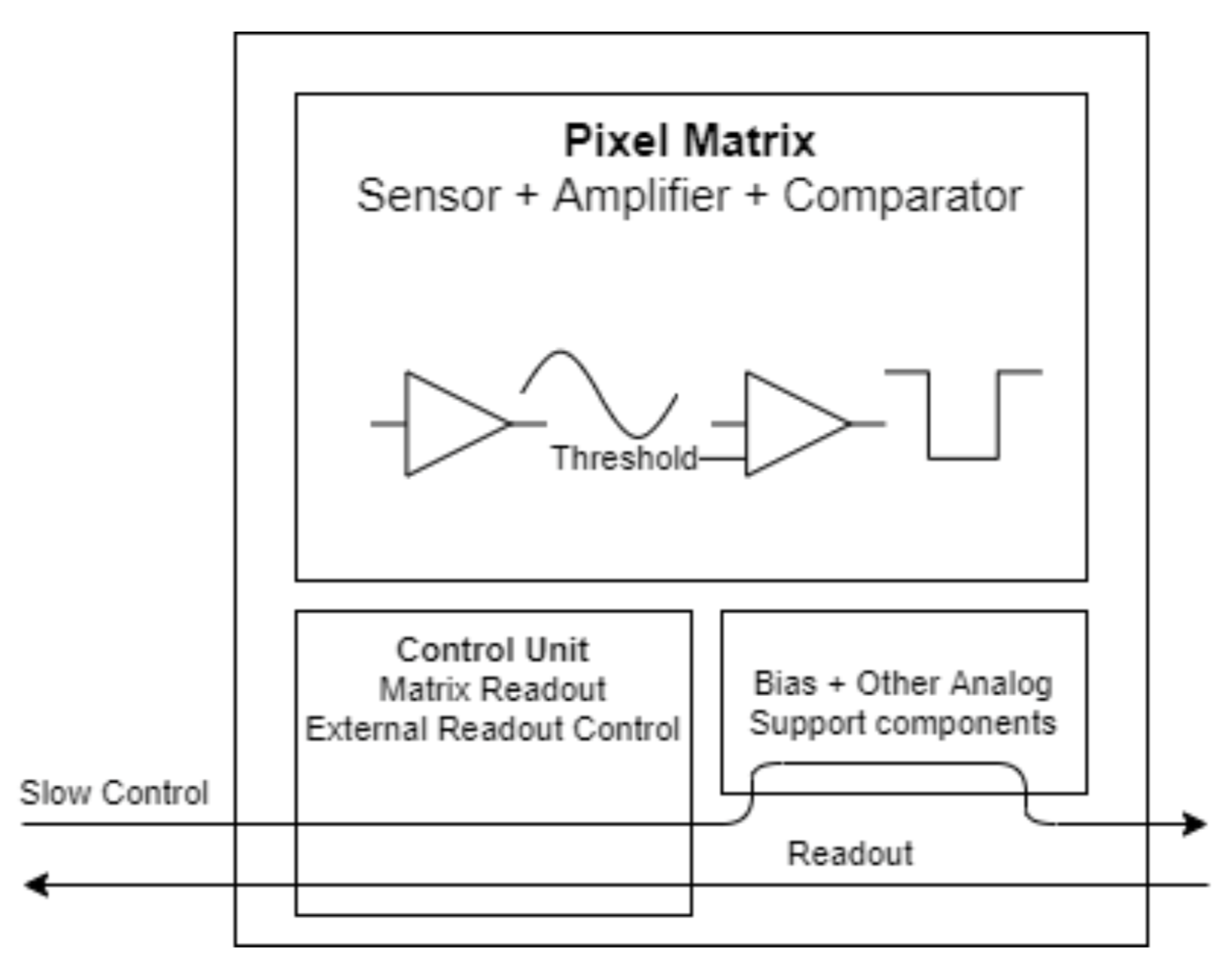
The next step in the development of a silicon detector for space is AstroPix, a monolithic high voltage complimentary metal-oxide semiconductor (HVCMOS) sensor. CMOS pixels perform charge collection, signal amplification, and readout with electronics all co-integrated into the pixel matrix (Fig. 3). The addition of a high voltage bias to every pixel enhances the charge collection efficiency over previous diffusion-based methods (Fig. 3(a)). At an individual pixel level, once the charge is collected, it is converted to a voltage signal by a charge sensitive amplifier, which goes into a comparator to generate a trigger above the threshold level. This signal is routed to the digital periphery of the chip (Fig. 3(b)) where the output from all pixels are digitized and read out [7]. In this way, two signals can be tested - the analog signal from individual pixels being the output of the charge-sensitive amplifier, and the fully digitized full-chip digital signal as readout from the digital periphery. This analog data is used in testing and characterization, but final AstroPix designs will exclusively utilize digital data readout.
An HVCMOS design such as AstroPix carries huge potential benefits over legacy technology in currently flying instruments. The CMOS fabrication process is common in commercial industry and well understood, making chip production affordable. Silicon is abundant, affordable, and operates at room temperature which further drives down costs. The CMOS design requires no readout ASIC board since the readout is done on-chip, easing integration and minimizing noise especially when compared to arrays of silicon strip detectors. The on-pixel circuitry is also customizable and low-power, creating sensors with less power per channel count relative to other pixelated or strip sensors.
An HVCMOS chip designed for use at the Large Hadron Collider’s ATLAS detector was first tested as a proof-of-concept study for AstroPix. This chip, called ATLASPix, utilized m2 pixels in four arrays of pixels. Local testing detailed in [2] showed that ATLASPix was a feasible starting point for AstroPix development.
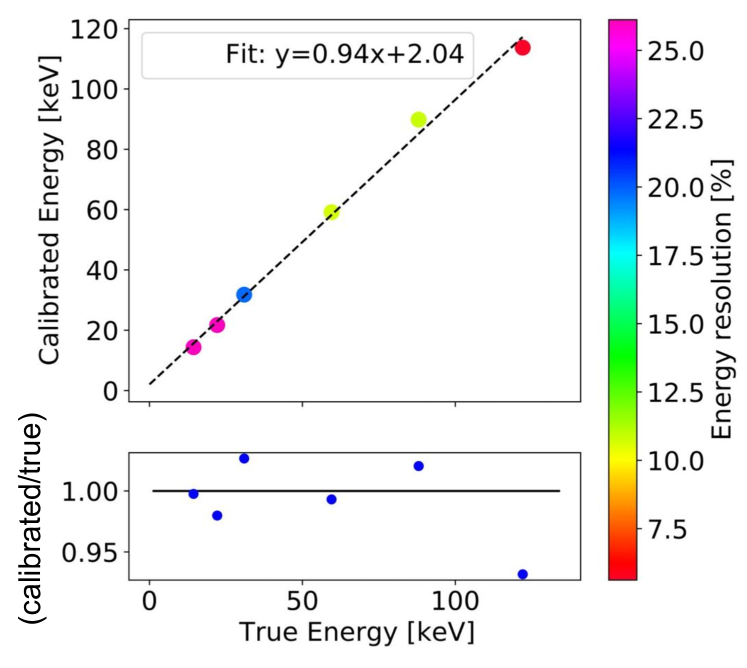
The space environment and type of incident particle that AstroPix is intended for differs greatly from those in the hadron collider that ATLASPix was designed for, so basic changes to the chip design had to be made. In stepping from ATLASPix to the first AstroPix chip, AstroPix_v1 or ‘version1’, the digital bit allocation for the time over threshold measurement (Section 2) was modified so that the precise nanosecond timing resolution was relaxed in favor of energy resolution. The pixels also increased in size. AstroPix_v1 was fabricated on 500 m thick silicon wafers with m2 in an array. Insufficient pixel shielding caused oscillations in the digital readout, so only analog data could be read out by AstroPix_v1. Studies from [10] detail charge injection studies, threshold studies, and energy calibration performed with AstroPix_v1. From one probed pixel, energy calibration from analog data was found to match known X-ray and gamma-ray sources within 6%. A maximum energy resolution (at FWHM, where where and are Gaussian fit parameters from a fit to the photopeak) of 25% (at 14 keV) was measured (Fig. 4(a)).

2 AstroPix_v2 Testing
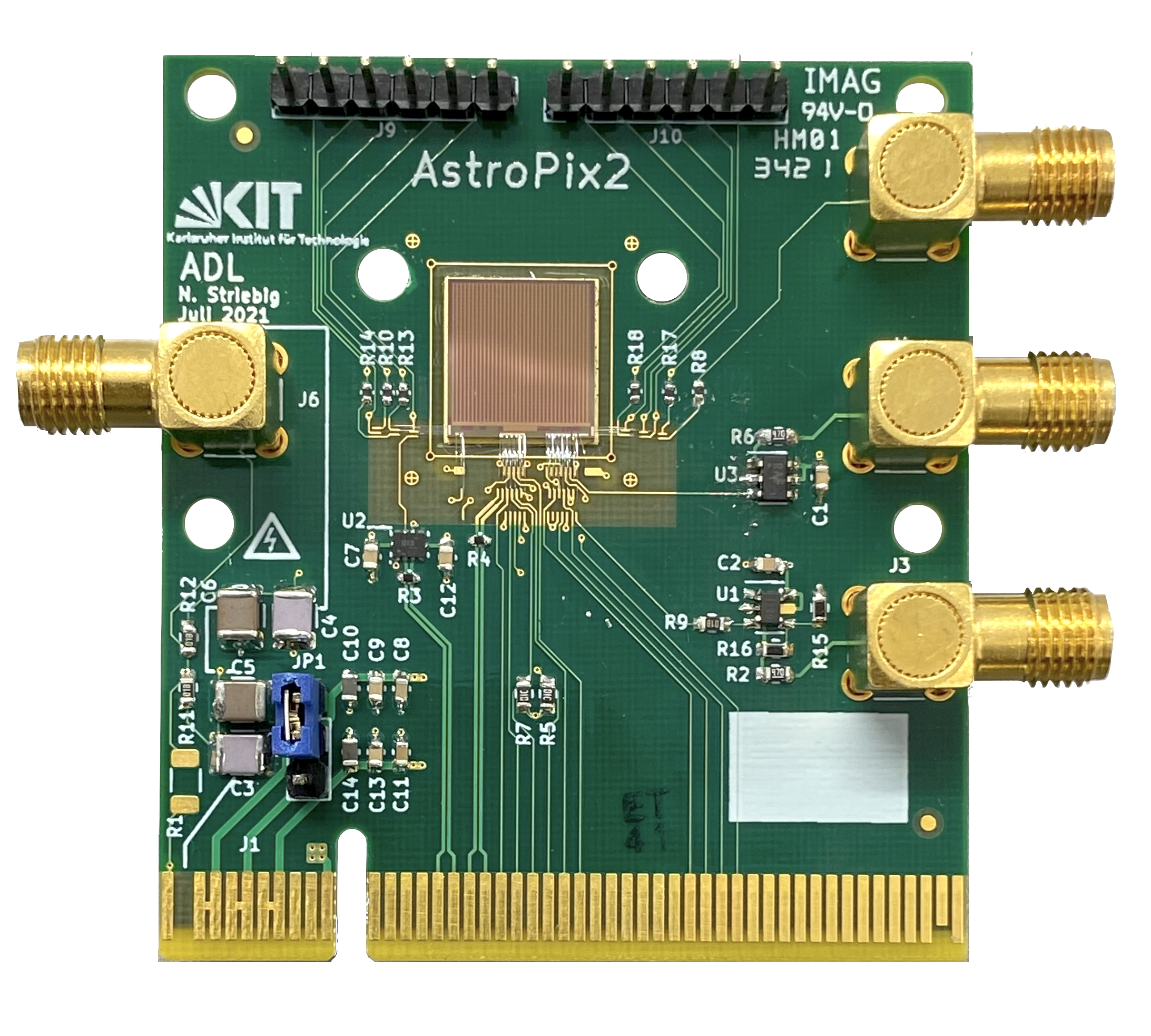
AstroPix_v2 aimed to incrementally move toward a flight prototype by fixing the shielding flaw and redesigning on-pixel circuitry to reduce power consumption. Pixels measure m2 in a array covering an area of cm2 (Fig. 5(a)). The guard ring design around each pixel was updated, allowing for higher bias voltages and deeper depletion of the 500 m wafer [10].
The performance of AstroPix_v2 was studied analogously to AstroPix_v1, where charge injection studies, threshold studies, and energy calibration was measured from the analog outputs of individual pixels (Fig. 5(b)). Energy calibration for AstroPix_v2 (Fig. 4(b)) is more precise than that of AstroPix_v1, where calibrated photopeak values matched the expected value within . AstroPix_v2 also measures better energy resolution for each calibrated point with a maximum energy resolution at 14 keV of 16% (25%) for AstroPix_v2 (AstroPix_v1).
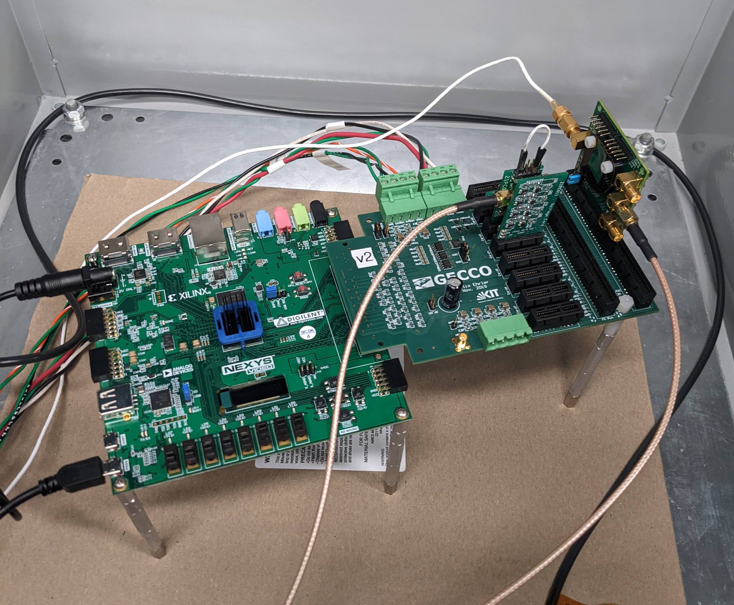
In order to test radiation hardness and performance in a relevant environment, AstroPix_v2 saw four test-beam campaigns - two at the Fermilab Test Beam Facility [1] with a 120 GeV proton beam and two at the Berkeley 88-Inch Cyclotron [5] with a cocktail of ions up to a linear energy transfer value of 65 MeV cm2/mg. Measurements made during both campaigns confirmed that no catastrophic latchup occurred during running - a state of inactivity where an incident particle triggers a parasitic thyristor, resulting in a short circuit, which can result in runaway current draws and the subsequent destruction of the device. Closer analysis is still underway from the radiation testing with ion beams to determine whether AstroPix_v2 experienced single event functional interrupt events, where single bits would have been flipped or corrupted by an ion interaction [10]. The testing in this extreme flux environment also resulted in improved data collection software.
Further details of the design changes from AstroPix_v1 to AstroPix_v2, analog performance and tests, and radiation testing can be found in [10].
A major correction from AstroPix_v1 to AstroPix_v2 was the ability to access digital data. While analog data can only be collected from a handful of select pixels, digital data is available from the whole array and is digitized on-chip for readout. In order to save on power and bandwidth, AstroPix_v2 reads out only row and column information rather than individual pixels, where individual pixel outputs are OR’ed together. In this way, only two channels (row and column) are sent from the array to the digital periphery. The digitized data is returned as an encoded bit stream containing information regarding the time of each hit, whether it is a row or column hit, the location of the row or column, and a Time over Threshold (ToT) measurement. Rather than associating the height of a voltage pulse with the deposited charge, as is done with analog analysis, the digitization requires the input of some voltage threshold and correlates the deposited charge to the amount of time that the resulting voltage pulse was over the threshold. A larger ToT is associated with a larger charge deposit.
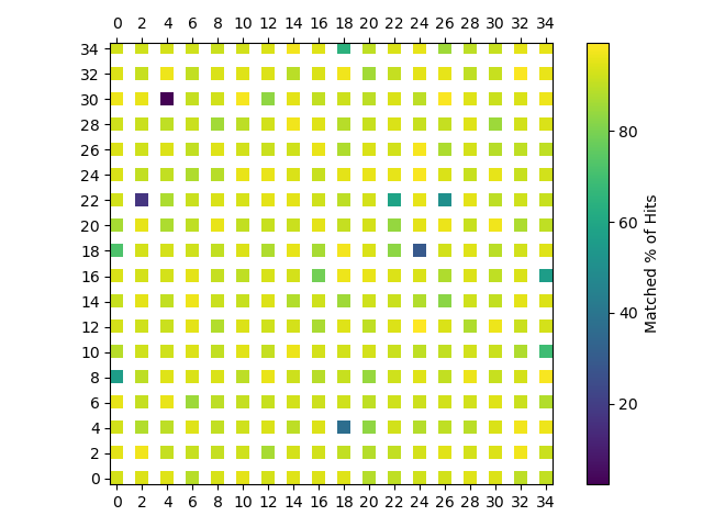
In this way, the activation of one pixel should return two digitized hits - one for the measurement of charge in the row, and a separate hit for the column. If corresponding to the same event, these hits must also match in time and measured ToT. This level of correlation was tested with an injected charge administered individually to a sample of pixels around the full array (Fig. 6). Each pixel was probed 140 times with an injected charge and the fraction of events where two paired row and column hits were recorded is plotted. 99% of probed pixels read out data where more than 80% of injections contain matching row and column hits, showing a very high correlation between row and column hits as expected. There is also no noted trend around the array of non-correlating pixels, indicating no large issues with chip fabrication or bonding to its custom printed circuit board. Pixels with poor coincidence may have large rates of noise, confusing the coincidence matching or overwhelming the trigger. Pixels such at these will be masked for data collection campaigns. Future iterations of AstroPix (Section 3) will record every pixel individually without OR’ing rows and columns, thus simplifying this problem and eliminating the need for postprocessing coincidence matching.
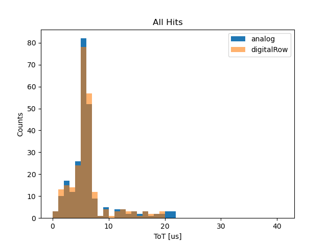
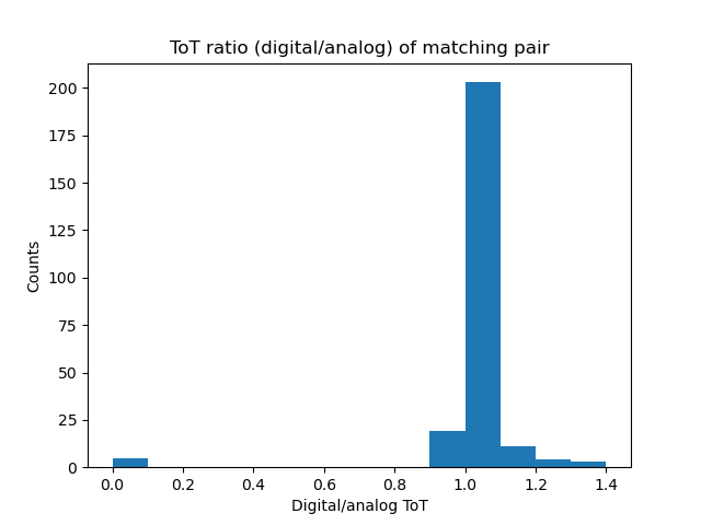
One way to verify the digital circuitry and configuration settings is to measure the analog signal at the same time. The analog signal is read after passing through a lowpass filter while the full digital signal is also passed through a highpass filter, but an incident particle should generate both an analog and a digital signal with nearly identical ToT measurements (or a ToT-proxy measurement as calculated from the shape of the analog voltage pulse). The corner pixel, row 0 column 0, alone was activated on the array and exposed to a 0.01 Ci Barium-133 source for 30 minutes. Post-processing software was designed to consider both the output analog and digital data sets, coincide the data in time in order to identify events that triggered both analog and digital readout, and finally to plot this coincident data. Though more analog hits were recorded than digital hits (with a data collection rate of 0.217 Hz compared to 0.162 Hz), 90.6% of digital data had a corresponding analog hit within a timing window of 0.07 s. The digital ToT measurements of these hits is matched very closely to the corresponding analog ToT-proxy measurement (Fig. 7), indicating that chip configuration settings are properly optimized. The timing window of 0.07s was derived as an optimal value from the data and reflects the large latency associated with the analog data collection method - it is not indicative of the inherent timing resolution of the chip.
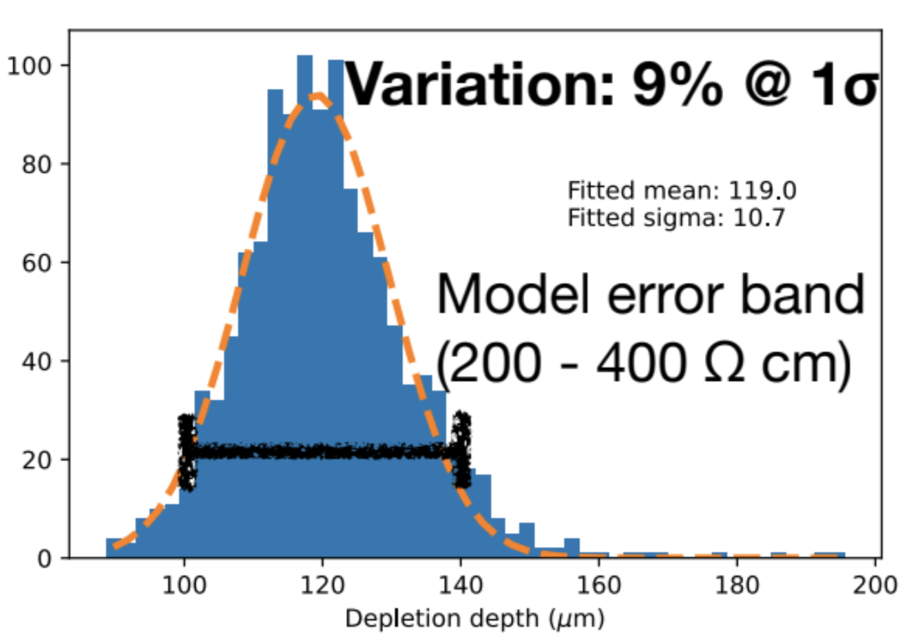
This digital output was also used to make a first measurement of depletion depth with AstroPix_v2. The AstroPix design utilizes a thick 500 m wafer and HV bias voltage into order to facilitate a large dynamic range of 25-700 keV. In order to achieve this full depletion, high resistivity wafers of 5 kcm will be utilized but the chips currently under test utilize 300 cm silicon so a smaller depletion depth and therefore dynamic range is expeted.
In order to measure the depletion depth of this lower resistivty array, individual pixels were probed with an Americium-241 source (photopeak at 59.5 keV) and -160V bias voltage. The source is assumed to be point-like, and it is assumed that there is no absorption. A depletion depth is calculated from the detection rate,
where is the nuclear decay rate (1 MBq), is the emission probability of 59.5 keV, is the number density of silicon, and is the photoelectric cross section of 59.5 keV in silicon. The geometric factor relates to the pixel size and source distance from the array. The detection rate is found by integrating the measured spectrum of the Americium source.
These direct measurements from every individual pixel of this lower resistivity array show that the depletion achieved with a -160V bias voltage is, on average, 119 m with a 9% variation at (Fig. 8). The -160V bias value was chosen due to the event rate maximizing and saturating at this bias. Final AstroPix designs will fully deplete 500 m in high-resistivity wafers, and this measured level of depletion on low-resistivity chips offers a promising start.
This value, and the depletion curve over a range of bias values, follows the shape of the model of a p-substrate sensor where
where is the permittivity F/cm, is hole mobility (500 cm2/s/V), is the sensor resistivity of 300 cm, and is a built-in potential of 0.6 V. At the time of writing, a systematic offset is found between the model prediction and data such that the data agrees more closely with the modeling of an n-substrate sensor where is the electron mobility of 1500 cm2/s/V. Work is underway to further understand this effect.
3 Ongoing work and Next Steps
Testing of AstroPix_v2 is still underway, with a current emphasis on digital data read out from the full array. There is also active testing of AstroPix_v2 fabricated on silicon wafers with high resistivity. This higher resistivity of 5 kcm as compared to the 300 cm wafers utilized for the data thus far presented should allow for larger depletion depth and therefore enhanced charge collection and dynamic range. AstroPix_v2 will see another Fermilab Test Beam Facility campaign in early 2023 with emphasis on multiple-layer readout utilizing multiple AstroPix_v2 chips in the beamline and testing preliminary particle tracking software.
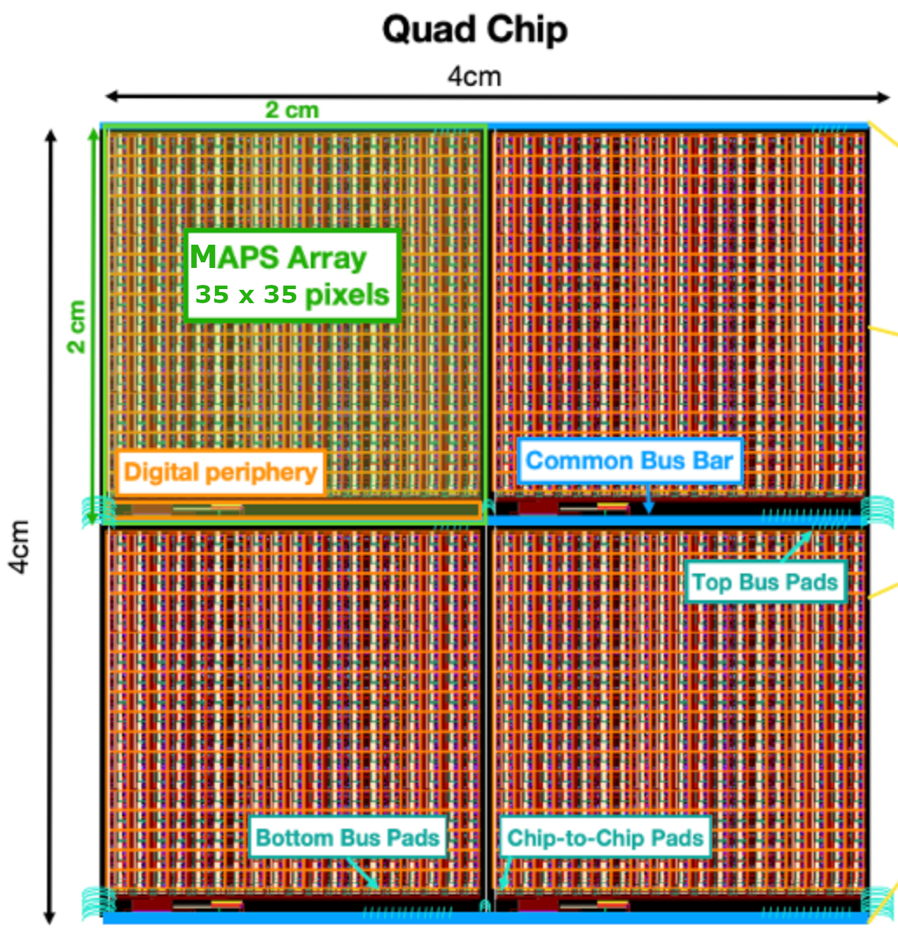
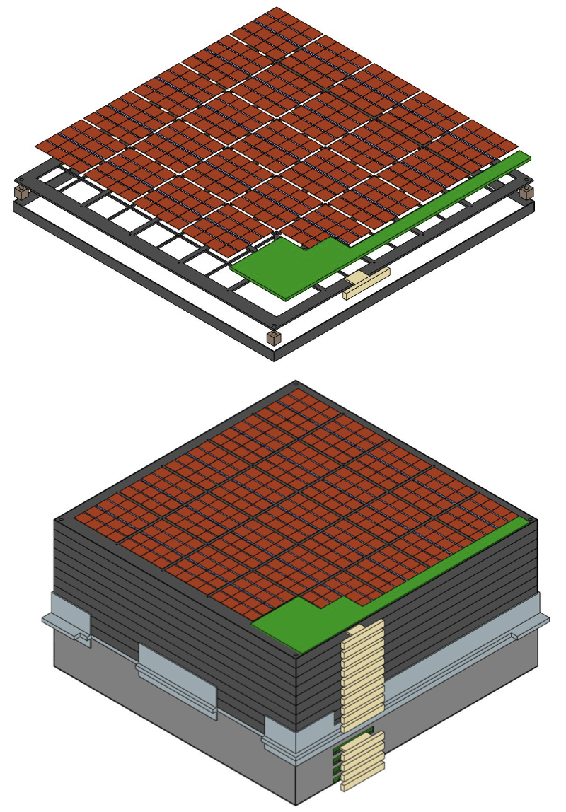
Concurrently, the AstroPix project continues to look ahead with the design of AstroPix_v3. This is a flight-protype version with a array of m2 pixels with a m2 active area. The continued increase in pixel size does not impact the energy resolution of future missions and allows AstroPix to consume less power and bandwidth with a smaller number of channels overall. However, the larger pixels create engineering challenges - for example, the large active area creates high capacitance levels which increase noise. The AstroPix_v3 strategy of reducing the active pixel area with respect to the pixel pitch avoids these complications. AstroPix_v3 will also be diced from the wafer as a cm2 quad chip, where four AstroPix_v3 arrays will be connected through common bus bars (Fig. 9(a)). AstroPix_v3 was delivered from the foundry in January 2023 and testing began shortly thereafter.
The AstroPix_v3 quad chip will be used on the Astropix Sounding rocket Technology dEmonstration Payload (A-STEP), currently scheduled for launch in late 2024. The 2U payload will consist of three layers of AstroPix_v3 quad chips with a thin aluminum housing (Fig. 9(b)), along with supporting electronics. A sounding rocket flight of roughly 10 minutes will take A-STEP 500 km above ground and provide the opportunity to measure cosmic rays and gamma rays. The project intention is to demonstrate functionality of the AstroPix sensors in a relevant space environment by reconstructing these charged particle tracks. The A-STEP project kicked off in October 2022 led through Goddard Space Flight Center with support from Wallops Flight Facility engineering support and the Sounding Rocket Program Office for coordination and planning.
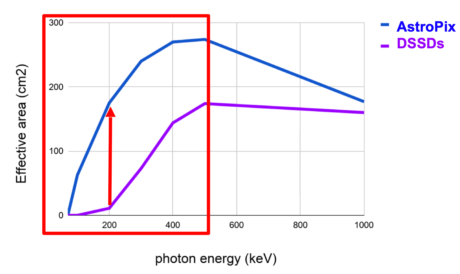
AstroPix is a mission enabling technology for future large-scale gamma-ray instruments. It is implemented in the 2021 MIDEX concept AMEGO-X as the main detector of the tracking subsystem [4]. The AMEGO-X tracker design features four identical towers of 40 layers of AstroPix with 95 quad chips per layer (Fig. 10(a)). The use of AstroPix at this scale provides AMEGO-X a significant improvement of effective area at low energies (50-500 keV) over that with the use of double sided silicon strip detectors (Fig. 10(b)).
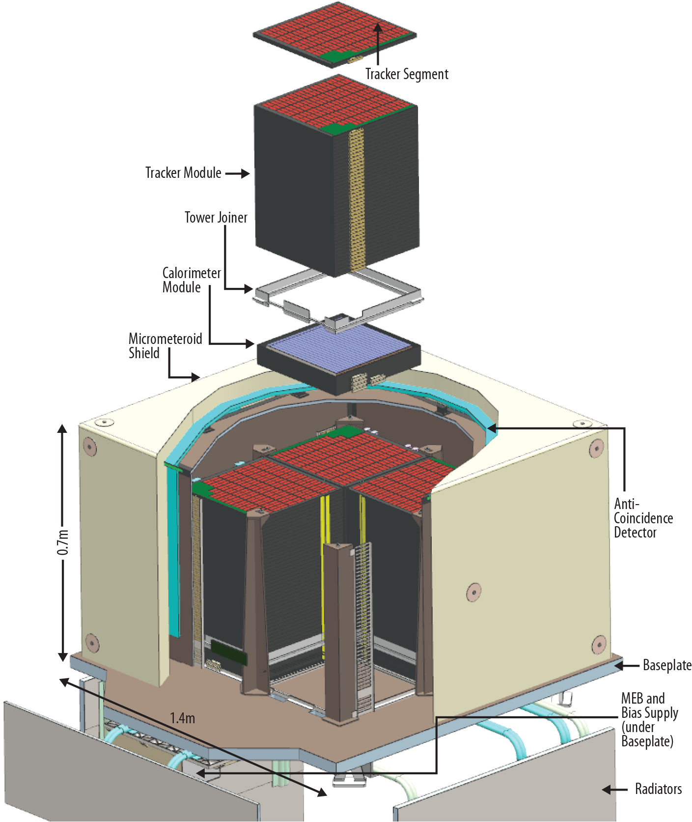
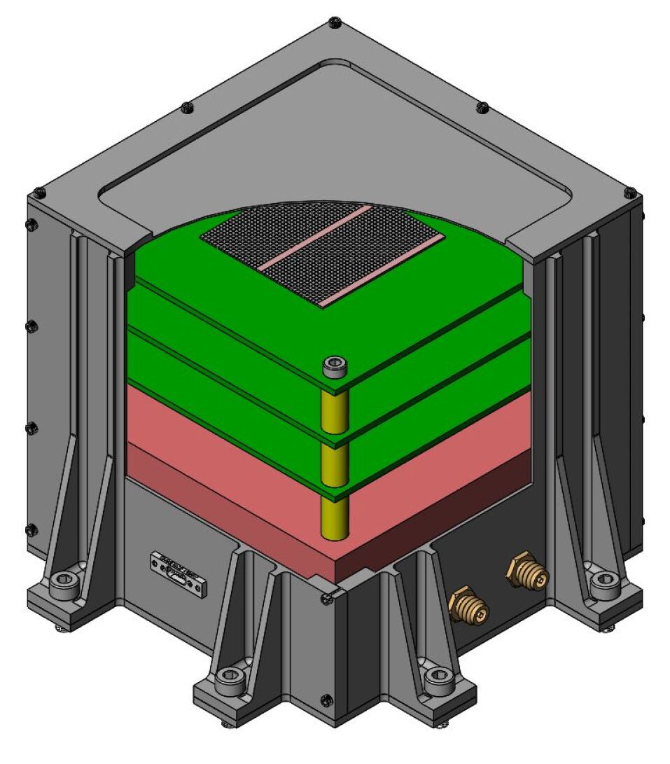
In order to build to full implementation in AMEGO-X, an AMEGO-X prototype is planned. This prototype is a combination of many efforts, including: AstroPix (as a novel tracker), a cesium-iodide calorimeter, the ComPair balloon instrument [9], and Compton event reconstruction improvements. The AMEGO-X prototype (Fig. 11), a next-generation ComPair instrument, will be one tower of the AMEGO-X instrument (though with less AstroPix tracker layers). The aim is to demonstrate operation of the full system in a relevant environment.
These implementations will also utilize future versions of AstroPix. AstroPix_v4 is currently in development with planned upgrades to the ToT readout system, and individual pixel readout (without row and column OR’ing) and threshold tuning.
4 Summary and Outlook
Future large-scale gamma-ray instruments, as prioritized by the Astro2020 Decadal Survey, will benefit from new technologies that allow for measurements with low noise and precise position and energy resolution. As an HVCMOS sensor, AstroPix serves as mission-enabling technology for these next-generation instruments. With development rooted in work done by the collider-based particle physics community, AstroPix has now realized two design iterations with a third recently delivered at the time of writing. The sensors are capable of analog and digital data readout and measure energy resolutions from analog data better than 16% at 14 keV in the most recent design iteration, AstroPix_v2. Digital readout is being tested with AstroPix_v2, where individual pixels are returning triggered data uniformly around the array as expected. The next design iteration, AstroPix_v3, will be diced as a quad chip sharing common readout of four individual arrays connected via a common bus bar and be utilized in future technology demonstrations including the sounding rocket payload A-STEP and AMEGO-X prototype ComPair balloon instrument.
The international AstroPix team spans three countries over five institutions with more than half of the contributors being early career scientists or engineers (including students). The team looks forward to continued testing of AstroPix, future development, and further implementation in next-generation space-based instruments.
References
- [1] Fermilab test beam facility. https://ftbf.fnal.gov/. Accessed: 2022-07-20.
- [2] Isabella Brewer, Michela Negro, Nicolas Striebig, Carolyn Kierans, Regina Caputo, Richard Leys, Ivan Peric, Henrike Fleischhack, Jessica Metcalfe, and Jeremy Perkins. Developing the future of gamma-ray astrophysics with monolithic silicon pixels. Nucl. Instrum. Meth. A, 1019:165795, 2021.
- [3] R. Caputo, Y. Fukazawa, R. P. Johnson, F. Longo, M. Prest, H. Tajima, and E. Vallazza. Silicon Detectors for Gamma-Ray Astronomy, pages 1–29. Springer Nature Singapore, Singapore, 2022.
- [4] Regina Caputo, Marco Ajello, Carolyn A. Kierans, Jeremy S. Perkins, Judith L. Racusin, Luca Baldini, Matthew G. Baring, Elisabetta Bissaldi, Eric Burns, Nicholas Cannady, Eric Charles, Rui M. Curado da Silva, Ke Fang, Henrike Fleischhack, Chris Fryer, Yasushi Fukazawa, J. Eric Grove, Dieter Hartmann, Eric J. Howell, Manoj Jadhav, Christopher M. Karwin, Daniel Kocevski, Naoko Kurahashi, Luca Latronico, Tiffany R. Lewis, Richard Leys, Amy Lien, Lea Marcotulli, Israel Martinez-Castellanos, Mario Nicola Mazziotta, Julie McEnery, Jessica Metcalfe, Kohta Murase, Michela Negro, Lucas Parker, Bernard Phlips, Chanda Prescod-Weinstein, Soebur Razzaque, Peter S. Shawhan, Yong Sheng, Tom A. Shutt, Daniel Shy, Clio Sleator, Amanda L. Steinhebel, Nicolas Striebig, Yusuke Suda, Donggeun Tak, Hiro Tajima, Janeth Valverde, Tonia M. Venters, Zorawar Wadiasingh, Richard S. Woolf, Eric A. Wulf, Haocheng Zhang, and Andreas Zoglauer. All-sky Medium Energy Gamma-ray Observatory eXplorer mission concept. Journal of Astronomical Telescopes, Instruments, and Systems, 8(4):044003, 2022.
- [5] M.A. McMahan. Radiation effects testing at the 88-inch cyclotron. In 1999 Fifth European Conference on Radiation and Its Effects on Components and Systems. RADECS 99 (Cat. No.99TH8471), pages 142–147, 1999.
- [6] National Academies of Sciences, Engineering, and Medicine. Pathways to Discovery in Astronomy and Astrophysics for the 2020s. The National Academies Press, Washington, DC, 2021.
- [7] Ivan Perić and Niklaus Berger. High Voltage Monolithic Active Pixel Sensors. Nucl. Phys. News, 28(1):25–27, 2018.
- [8] A. Schöning, J. Anders, H. Augustin, M. Benoit, N. Berger, S. Dittmeier, F. Ehrler, A. Fehr, T. Golling, S. Gonzalez Sevilla, J. Hammerich, A. Herkert, L. Huth, G. Iacobucci, D. Immig, M. Kiehn, J. Kröger, F. Meier, A. Meneses Gonzalez, A. Miucci, L. O. S. Noehte, I. Peric, M. Prathapan, T. Rudzki, R. Schimassek, DMS Sultan, L. Vigani, A. Weber, M. Weber, W. Wong, E. Zaffaroni, and H. Zhangh. Mupix and atlaspix – architectures and results, 2020.
- [9] Daniel Shy, Carolyn Kierans, Nicolas Cannady, Regina Caputo, Sean Griffin, J. Eric Grove, Elizabeth Hays, Emily Kong, Nicholas Kirschner, Iker Liceaga-Indart, Julie McEnery, John Mitchell, A. A. Moiseev, Lucas Parker, Jeremy S. Perkins, Bernard Phlips, Makoto Sasaki, Adam J. Schoenwald, Clio Sleator, Jacob Smith, Lucas D. Smith, Sambid Wasti, Richard Woolf, Eric Wulf, and Anna Zajczyk. Development of the ComPair gamma-ray telescope prototype. In Jan-Willem A. den Herder, Shouleh Nikzad, and Kazuhiro Nakazawa, editors, Space Telescopes and Instrumentation 2022: Ultraviolet to Gamma Ray, volume 12181, page 121812G. International Society for Optics and Photonics, SPIE, 2022.
- [10] Amanda L. Steinhebel, Henrike Fleischhack, Nicolas Striebig, Manoj Jadhav, Yusuke Suda, Ricardo Luz, Carolyn Kierans, Regina Caputo, Hiroyasu Tajima, Richard Leys, Ivan Peric, Jessica Metcalfe, and Jeremy S. Perkins. AstroPix: novel monolithic active pixel silicon sensors for future gamma-ray telescopes. In Jan-Willem A. den Herder, Shouleh Nikzad, and Kazuhiro Nakazawa, editors, Space Telescopes and Instrumentation 2022: Ultraviolet to Gamma Ray, volume 12181, page 121816Y. International Society for Optics and Photonics, SPIE, 2022.
- [11] Nicolas Striebig. Development of integrated sensors for gamma ray astronomy. Master’s thesis, Karlsruhe Institute of Technology, 2021.