[a]Christian Bespin
Charge collection and efficiency measurements of the TJ-Monopix2 DMAPS in 180 nm CMOS technology
Abstract
Monolithic CMOS pixel detectors have emerged as competitive contenders in the field of high-energy particle physics detectors. The use of commercial processes offers high-volume production of such detectors. A series of prototypes has been designed in a Tower CMOS process with depletion of the sensor material and a column-drain readout architecture. The latest iteration, TJ-Monopix2, features a large matrix consisting of pixels with pitch. A small collection electrode design aims at low power consumption and low noise while the radiation tolerance for high-energy particle detector applications needs extra attention. With a goal to reach radiation tolerance to levels of NIEL damage of , a modification of the standard process has been implemented by adding a low-dosed n-type silicon implant across the pixel in order to allow for homogeneous depletion of the sensor volume. Recent lab measurements and beam tests were conducted for unirradiated modules to study electrical characteristics and hit detection efficiency.
1 Introduction
In recent years, advances in CMOS technologies have fueled the development of a new generation of monolithic active pixel sensors (MAPS) with fast readout and high radiation tolerance by depleting the charge sensitive volume [1]. These depleted MAPS (DMAPS) devices are therefore an interesting candidate for high-energy particle physics experiments with high radiation environments and high particle rate. Depletion is achieved by either using high-voltage add-ons in the CMOS technology and/or high resistivity substrates. The increasing availability of these features in commercial CMOS processes could combine the features of the detector concept with possibly faster and cheaper production than common hybrid pixel detectors for the mentioned purposes. The idea behind and measurements results from one of multiple DMAPS prototypes, TJ-Monopix2 [2, 3], will be presented in the following.
2 Design of TJ-Monopix2
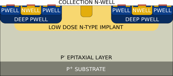
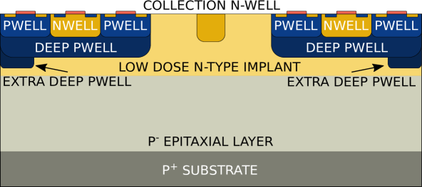
TJ-Monopix2 is the latest DMAPS prototype from the TJ-Monopix development line which is based on the ALPIDE pixel detector developed for the ALICE ITS upgrade [4]. It is fabricated in the same commercial CMOS process provided by Tower Semiconductor111https://towersemi.com. A modification of the process used for ALPIDE has been implemented to increase the radiation tolerance to levels by adding a low dose n-type implant for homogeneous growth of the depletion zone with applied bias voltage. In measurements on first prototypes with this modification, a drop in hit detection efficiency was observed after irradiation [5, 6]. This could be improved significantly by adding a gap in the n-type blanket or a deep p-type implant in the pixel corners to shape the electrical field towards the collection electrode [7]. The cross-sections of these two sensor designs is shown in fig. 1.
Additionally, chips have been produced on Czochralski silicon to increase the available depletable volume compared to the thickness of the epitaxial layer (). Measurements on Czochralski silicon chips in TJ-Monopix1 showed a further increase in hit detection efficiency after irradiation [8].
TJ-Monopix2 follows a small collection electrode approach with a pixel capacitance of about . The pixels of size are read out using an established synchronous column-drain technique from the FE-I3 readout chip [9]. Further changes from the predecessor TJ-Monopix1 include an improved front-end design, a new pixel masking scheme and a 3-bit DAC for local threshold tuning. With these changes the threshold is expected to be reduced by a factor of while improving the threshold dispersion and noise behavior.
The digital periphery contains logic for register configuration, data handling and LVDS output drivers. Slow control is done via a command protocol and decoder that was taken from the RD53B readout chip [10]. Both pixel and register data is 8b10b encoded in a frame-based data stream which allows operating the chip with four differential data lines.
3 Injection-based threshold and noise measurements
Initial tests have been performed in a laboratory setup to measure the threshold and noise performance of TJ-Monopix2. All of these values are extracted from injecting different amounts of charge into the pixel a given number of times and recording the amount of registered hits . The response function is a smeared step function of the form
| (1) |
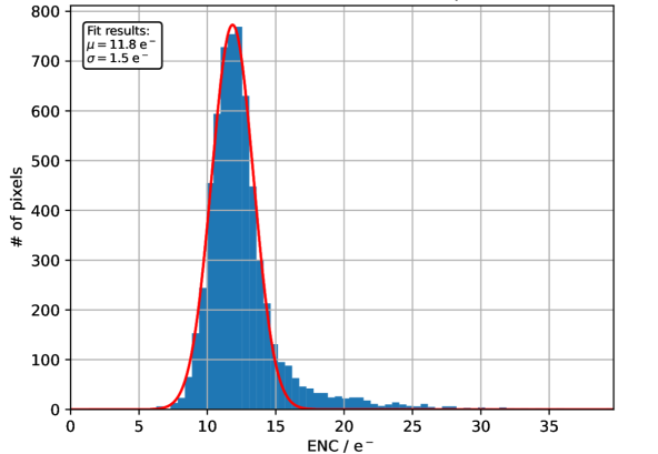
with the injected charge amount, the number of consecutive injections of and the charge at the threshold. denotes the gaussian smearing of the step function which is defined as the electronic noise of the pixel. The threshold is defined as the charge at which of the injected hits are recorded from the pixel. Histogramming the individual thresholds from each pixel leads to the distribution shown in fig. 2(a).
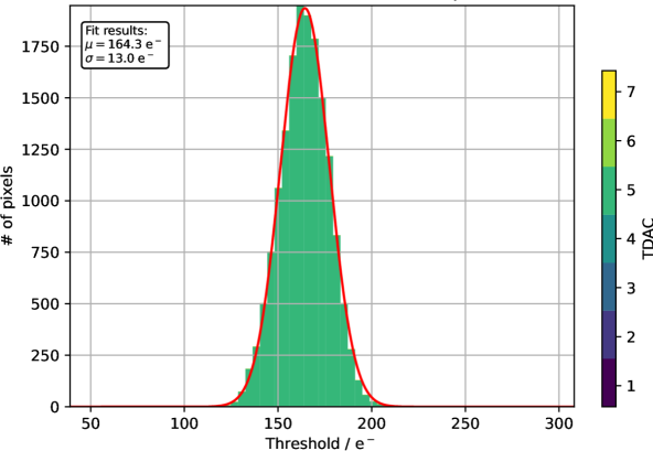
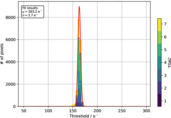
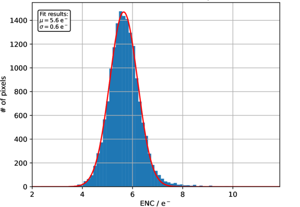
The distribution has a mean value of and a width of which is defined as the threshold dispersion. By adjusting the threshold DAC in each pixel in order to even out the deviations from the target threshold, the threshold dispersion can be reduced significantly. The resulting distribution after this so-called tuning process is shown in fig. 2(b). While the mean threshold stays basically the same, the dispersion could be reduced by a factor of almost . Both the mean threshold and threshold dispersion are significantly lower than in TJ-Monopix1, where losses in hit detection efficiency could be observed due to too large thresholds [8].
The corresponding histogram of the electronic noise is depicted in fig. 3.
As a comparison, the distribution from the predecessor TJ-Monopix1 is included, where a large tail towards higher values was observed that led to a high operational threshold in order to limit the amount of noisy pixels. It can be seen, that this tail is largely removed with slight changes to the analog front-end, which in turn lowers the threshold for a regular operation of the chip.
4 Hit detection efficiency measurements
Two different pixel variations were investigated regarding their hit detection efficiency, that will be presented in the following – a DC-coupled, more standard design which makes up most part of the matrix and an AC-coupled investigative design realized in only a few columns of the matrix. While the former was measured in more detail, some first results of the latter are included as well.
4.1 Standard DC-coupled pixel flavor
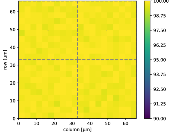
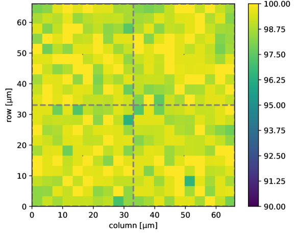
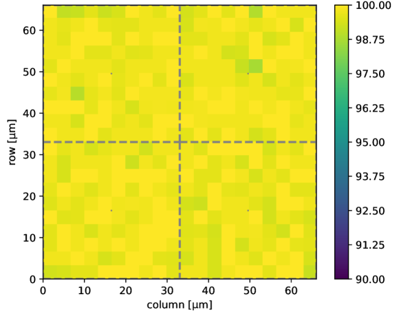
First measurements to determine the hit detection efficiency have been performed in a electron beam at the DESY II testbeam facility at DESY, Hamburg [11]. Three unirradiated modules were tested with different sensor geometries: two chips with thick epitaxial silicon and the two geometries depicted in fig. 1 as well as one chip built on Czochralski silicon with a gap in the low dose n-type implant (see fig. 1(a)). It should be noted that the different substrate materials offer different sensor thicknesses and therefore charge-sensitive volume depending on the depletion. The measurements are not targeting a comparison between different types of silicon.
Figures 4(a) and 4(b) show the recorded cluster charge for a chip with epitaxial layer and with Czochralski substrate.
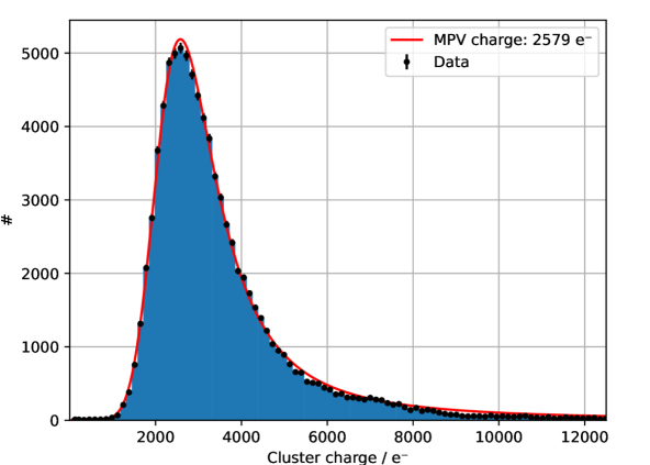
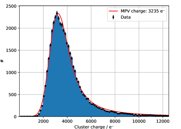
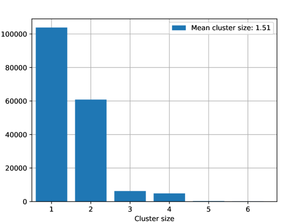
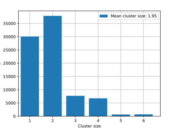
It can be observed that the collected charge is about larger in the Cz sample, because the depletion depth is only limited by the thickness of the sensor () which is by far not fully depleted, but more depleted than the thick epitaxial layer in the other chip.
The average cluster size is significantly larger in the Cz sample as well which results in a high spatial resolution due to charge-weighted clustering. The cluster size distributions for the same samples as above are depicted in figs. 4(c) and 4(d). While cluster size is predominant in the epitaxial sample, the Cz sample has mainly clusters of size . The corresponding average cluster size is and , respectively. Taking the pointing resolution of the beam telescope into account, an intrinsic spatial resolution of could be achieved in a Czochralski silicon sample.
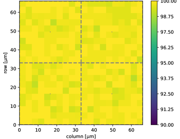
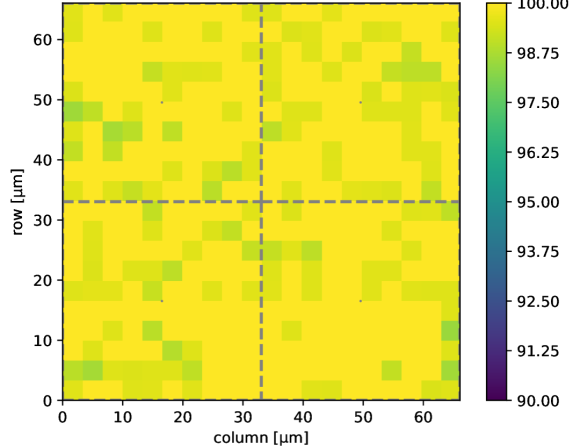
The hit detection efficiency was measured with a beam telescope with six Mimosa26 planes and a FE-I4 time reference plane which are all connected to a trigger logic unit to synchronize individual detector hits time-wise. The efficiency for all three modules is shown in fig. 5 where the result for every pixel was mapped onto a two by two pixel cell to increase the statistics to see possible effects or efficiency losses within a single pixel. All samples were running at a threshold of about and achieve a hit detection efficiency around with slight deviations within the error (estimated ). There are no losses observable in the pixel corners or between pixels.
4.2 AC-coupled pixel flavor
Another pixel variation with different analog front-end was tested as well to determine its performance in a particle beam. In this design the (positive) bias voltage is applied via a diode on the top side of the chip and connected to the charge collection n-well. To avoid breakdown of the front-end electronics due to the high voltage () on that well, the input signal is AC coupled to the amplifier. This approach can potentially deplete the substrate further due to the higher voltage than what can be applied in the standard pixel design. The hit detection efficiency was measured for different bias voltages and is shown in fig. 6.
At the efficiency is already above and reaches the same value as for the DC coupled pixel flavor of at or before bias voltage. This is, taking the slightly higher threshold into account, in agreement with the expectation that there should be no noticeable difference in hit detection efficiency before irradiation between the two pixel flavors. The larger applicable bias voltage could prove superior after irradiation to achieve more depletion and therefore higher charge signal.
5 Conclusion
In summary, the performance of TJ-Monopix2 shows a significant improvement in threshold value and dispersion compared to TJ-Monopix1, although the former is higher than its design value (). With the measured amount of charge in the sensor the threshold is still small enough to detect a majority of hits even from large clusters before irradiation. The large signal compared to the small pixel leads to a large cluster size and therefore high spatial resolution, where chips on Czochralski substrate perform slightly better due to the larger sensor volume. For the tested sensor materials with different thicknesses and sensor geometries, the hit detection efficiency is around or better in all cases. The modified front-end version with bias applied on the charge collection node achieves similar values for the hit detection efficiency while providing a larger headroom in bias voltage to achieve efficient performance after radiation damage. The results for irradiated modules will be presented in a forthcoming publication.
Acknowledgments
This project has received funding from the Deutsche Forschungsgemeinschaft DFG (grant WE 976/4-1), the German Federal Ministry of Education and Research BMBF (grant 05H15PDCA9), and the European Union’s Horizon 2020 research and innovation program under grant agreements no. 675587 (Maria Sklodowska-Curie ITN STREAM), 654168 (AIDA-2020), and 101004761 (AIDAinnova). The measurements leading to these results have been performed at the Test Beam Facility at DESY Hamburg (Germany), a member of the Helmholtz Association (HGF).
References
- [1] I. Perić, A novel monolithic pixelated particle detector implemented in high-voltage CMOS technology, Nuclear Instruments and Methods in Physics Research Section A: Accelerators, Spectrometers, Detectors and Associated Equipment 582 (2007) 876.
- [2] K. Moustakas, M. Barbero, I. Berdalovic, C. Bespin, P. Breugnon, I. Caicedo et al., CMOS monolithic pixel sensors based on the column-drain architecture for the HL-LHC upgrade, Nuclear Instruments and Methods in Physics Research Section A: Accelerators, Spectrometers, Detectors and Associated Equipment 936 (2019) 604.
- [3] Konstantinos Moustakas, Design and Development of Depleted Monolithic Active Pixel Sensors with Small Collection Electrode for High-Radiation Applications, Ph.D. thesis, Rheinische Friedrich-Wilhelms-Universität Bonn, Sept., 2021.
- [4] M. Mager, ALPIDE, the Monolithic Active Pixel Sensor for the ALICE ITS upgrade, Nuclear Instruments and Methods in Physics Research Section A: Accelerators, Spectrometers, Detectors and Associated Equipment 824 (2016) 434 .
- [5] I. Caicedo, M. Barbero, P. Barrillon, I. Berdalovic, S. Bhat, C. Bespin et al., The Monopix chips: depleted monolithic active pixel sensors with a column-drain read-out architecture for the ATLAS Inner Tracker upgrade, Journal of Instrumentation 14 (2019) C06006.
- [6] C. Bespin, M. Barbero, P. Barrillon, I. Berdalovic, S. Bhat, P. Breugnon et al., DMAPS Monopix developments in large and small electrode designs, Nuclear Instruments and Methods in Physics Research Section A: Accelerators, Spectrometers, Detectors and Associated Equipment 978 (2020) 164460.
- [7] M. Dyndal, V. Dao, P. Allport, I.A. Tortajada, M. Barbero, S. Bhat et al., Mini-MALTA: radiation hard pixel designs for small-electrode monolithic CMOS sensors for the High Luminosity LHC, Journal of Instrumentation 15 (2020) P02005.
- [8] C. Bespin, I. Berdalovic, I. Caicedo, R. Cardella, J. Dingfelder, L. Flores et al., Development and characterization of a DMAPS chip in TowerJazz 180 nm technology for high radiation environments, Nuclear Instruments and Methods in Physics Research Section A: Accelerators, Spectrometers, Detectors and Associated Equipment 1040 (2022) 167189.
- [9] I. Perić, L. Blanquart, G. Comes, P. Denes, K. Einsweiler, P. Fischer et al., The FEI3 readout chip for the ATLAS pixel detector, Nuclear Instruments and Methods in Physics Research Section A: Accelerators, Spectrometers, Detectors and Associated Equipment 565 (2006) 178.
- [10] RD53 collaboration, RD53B Manual, Tech. Rep. CERN-RD53-PUB-19-002, CERN, Geneva (Mar, 2019).
- [11] R. Diener, J. Dreyling-Eschweiler, H. Ehrlichmann, I. Gregor, U. Kötz, U. Krämer et al., The DESY II test beam facility, Nuclear Instruments and Methods in Physics Research Section A: Accelerators, Spectrometers, Detectors and Associated Equipment 922 (2019) 265.