Proximity-enhanced valley Zeeman splitting at the WS2/graphene interface
Abstract
The valley Zeeman physics of excitons in monolayer transition metal dichalcogenides provides valuable insight into the spin and orbital degrees of freedom inherent to these materials. Being atomically-thin materials, these degrees of freedom can be influenced by the presence of adjacent layers, due to proximity interactions that arise from wave function overlap across the 2D interface. Here, we report 60 T magnetoreflection spectroscopy of the A- and B- excitons in monolayer WS2, systematically encapsulated in monolayer graphene. While the observed variations of the valley Zeeman effect for the A- exciton are qualitatively in accord with expectations from the bandgap reduction and modification of the exciton binding energy due to the graphene-induced dielectric screening, the valley Zeeman effect for the B- exciton behaves markedly different. We investigate prototypical WS2/graphene stacks employing first-principles calculations and find that the lower conduction band of WS2 at the valleys (the band) is strongly influenced by the graphene layer on the orbital level. This leads to variations in the valley Zeeman physics of the B- exciton, consistent with the experimental observations. Our detailed microscopic analysis reveals that the conduction band at the point of WS2 mediates the coupling between and graphene due to resonant energy conditions and strong coupling to the Dirac cone. Our results therefore expand the consequences of proximity effects in multilayer semiconductor stacks, showing that wave function hybridization can be a multi-step process with different bands mediating the interlayer interactions. Such effects can be exploited to resonantly engineer the spin-valley degrees of freedom in van der Waals and moiré heterostructures.
Keywords: TMDs, graphene, valley Zeeman effect, proximity
I. Introduction
Van der Waals layered materials allow for the assembly of intentionally designed stacks with a dedicated topology or functionality[1, 2, 3, 4, 5, 6]. A key concept in this regard are proximity effects, where properties of a material or an ordered state are transferred from one layer to another without strongly affecting its electronic structure[7]. Nevertheless, a direct overlap of the wave functions in the adjacent layers is required for the proximity effect to take place. For example, pristine graphene (Gr) is a gapless Dirac semimetal with a linear dispersion relation around the points and negligible spin-orbit coupling (SOC)[8] while proximity effects from adjacent materials may significantly tailor its properties to acquire a positive or negative mass[9], spin polarization and spin-orbit coupling[10, 11, 12, 13, 14, 15, 16] or superconductivity[17, 18, 19, 20].
In recent years, the interface of Gr with a monolayer transition-metal dichalcogenide (ML TMD) has received wide attention. This system provides the appealing situation of creating a heterojunction between a material with strong SOC (the ML TMD) and long spin lifetimes (Gr). With respect to spin physics, particular interest was given to the topic of proximity induced spin-orbit coupling in Gr due to the strong SOC of the TMD[11, 12, 13, 14, 15, 21, 22, 23, 9, 16, 24, 25, 26]. Typically, proximity effects in the Gr community are theoretically modeled as a perturbation to the low energy model Hamiltonian of the Dirac cone[3], while keeping the wave functions unmodified (taken as purely p orbitals in Gr).
From the perspective of the optical properties of ML TMDs, engineering the dielectric environment with hexagonal boron nitride[27, 28, 29, 30, 31, 32] or Gr[33, 34, 31], has been shown to be a very efficient path for tunable modification of the exciton binding energy () or sub nm lateral modulation of the TMD band gap ()[33, 35]. This unprecedented degree of freedom provides novel functionality with respect to lateral heterojunctions, a technological feature which is very hard to realize in conventional semiconductor technology. In terms of conventional semiconductor spin physics, changes in the band gap are associated with strong modifications of the band -factors, particularly in materials with strong SOC[36, 37, 38]. Therefore, it is expected that the ability to modify the band gap in the TMDs provides a path to tailor its exciton valley Zeeman effect. Recent state-of-the-art first principles calculations[39, 40, 41, 42] have shown how to properly evaluate the orbital angular momentum contribution to the exciton valley Zeeman effect in ML TMDs, taking into account the Bloch functions of conduction and valence band electrons. Interestingly, the exciton -factor depends only weakly on the band gap, while the band -factors are indeed more sensitive to [39], as expected from conventional III-V semiconductors within the k.p framework[43, 38]. While the valley Zeeman physics in intrinsic monolayers[39, 40, 41, 42, 44, 45, 46] and hetero/homo-bilayers[39, 42, 47, 48, 49, 50, 51] is relatively well understood based on the recent ab initio developments, the influence of finite carrier density[52, 53, 54, 55, 56, 57, 58] or the evolution of the (in-plane) spin and orbital degrees of freedom in multilayered van der Waals heterostructures[59] still require further work.
In this study, we systematically investigate the dependence of the 1s exciton valley Zeeman -factor on van der Waals heterostructures of monolayer WS2 with graphene. We performed circularly polarized magneto-reflection spectroscopy up to 60 T on large area films of ML WS2 grown by chemical vapor deposition (CVD). The films were transferred either directly on SiO2, or were single/double encapsulated with monolayer Gr. Clear valley splittings for the A- and B- excitons () are observed, providing measurements of the associated exciton -factors for each assembled structure. While the -factor of the varies smoothly and consistently with the band gap renormalization and size of the exciton wave function, surprisingly the -factor of varies more strongly in magnitude and distinctly non-monotonic. We explore the microscopic origin of this behavior with detailed first-principles calculations on several prototypical WS2/Gr heterostructures with different stacking, shifts and twist angles. We show that the WS2 conduction bands at the point mediate the interaction between the lower conduction band () at the point and the graphene Dirac cone, leading to distinct changes on the orbital degree of freedom of and, consequently, on the B- exciton -factor. This mediated coupling happens because of the energetic alignment of the conduction band and at , which is absent in Mo-based TMDs. Furthermore, our quantitative account of the dielectric screening effects of Gr to the exciton -factors (reduction of the band gap and localization of exciton wave function) strengthens our picture that the non-monotonic variations in are indeed signatures of the complex interlayer hybridization between WS2 and Gr. Our results therefore expand the concept of proximity effects, revealing that interlayer wave function hybridization of adjacent crystalline layers can happen at different levels (mediated by different energy bands), a concept that is crucial for understanding the spin-valley physics of van der Waals and moiré heterostructures.
II. Experimentally determined valley Zeeman effect in WS2/graphene systems
We depict a schematic of the experiment and the investigated sample stacks in Figure 1(a). Large-area monolayer films of WS2 were grown by CVD on SiO2/Si or graphene substrates[60, 61, 62]. The monolayer nature and high quality of these samples were confirmed by photoluminescence and Raman spectroscopy maps[63, 64, 65]. The as-grown monolayers were transferred from the growth substrate to a Si/SiO2 substrate via standard wet transfer methods. For the doubly graphene encapsulated WS2 layer, a top graphene layer was wet-transferred on the WS2/graphene CVD film on the target substrate. Magneto-reflectance studies were performed at cryogenic temperatures () in a capacitor-driven 65 T pulsed magnet at the National High Magnetic Field Laboratory in Los Alamos. Details about the experimental setup can be found in the Supplemental Note I[66] and in Ref.[27]. A total of three samples of each batch were investigated with two separate spots on each of the three samples. Data shown in this manuscript are typical for each batch and the reported error bars derive from averages of all experiments done on each batch.
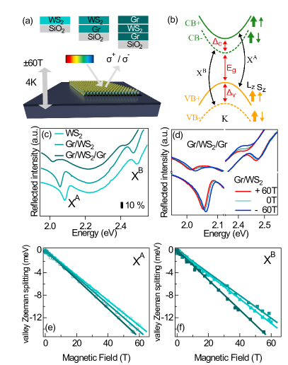
We investigate the effect of graphene encapsulation on the exciton binding energy and in particular the evolution of the valley Zeeman effect[67] of the A and B excitons, depicted in the single-particle energy diagram of the conduction and valence band in monolayer TMDs close to the point of the Brillouin zone [Fig. 1(b)]. These excitons are observed as dips in the smooth reflection spectra depicted in Fig. 1(c) close to 2.05 eV () and 2.45 eV (), respectively. No charged exciton features can be observed, confirming that the samples are close to intrinsic[68], although no active carrier control through gates has been employed here. The energy difference between and at zero magnetic field is given by the difference in the respective exciton binding energy and the SOC-induced splitting of the conduction () and valence band (). As mentioned in the introduction, graphene encapsulation successively introduces screening for the interband transitions in the TMD ML. This directly affects the band gap and , causing the excitonic transitions to shift with varying encapsulation [see Fig. 1(c)]. The effect of the increased screening on the 2D excitons can be probed in high field magnetospectroscopy.
In a magnetic field, the exciton energies shift following the relation
| (1) |
where the diamagnetic shift,
| (2) |
the reduced mass of the exciton is and the exciton ground state rms size is . is the valley index, is the Bohr magneton, and are the valley Zeeman -factors of the excitons, related to the relevant energy bands by
| (3) |
with being the out-of-plane g-factor of the Bloch band with wave vector [see the relevant bands in Fig. 1(b)].
| WS2 | Gr/WS2 | Gr/WS2/Gr | |
|---|---|---|---|
| -3.8 | -4.0 | -4.2 | |
| -3.7 | -3.3 | -4.5 | |
| -0.1 | -0.7 | 0.3 |
Figure Fig. 1(d) shows the reflection spectra of for the single and doubly Gr-encapsulated WS2 at zero and the maximum applied magnetic field. A valley Zeeman splitting of meV for each, resonance, analyzed in detail below, is observed. Both resonances shift to lower (higher) energy in positive (negative) fields, indicating a negative -factor. The spectral features were fit using complex (absorptive and dispersive) Lorentzian lineshapes to extract the transition energy. Although the exact position of each resonance at zero magnetic field is difficult to determine precisely due to the smoothly varying background, the magnetic field dependent shifts can be exactly determined, as the background is unaffected during the magnetic field pulse. As such, the diamagnetic shift and the valley Zeeman splitting can be simply determined from the average and difference of the exciton -dependent shift in positive and negative fields. In the Supplemental Note II - IV[66], we provide further details of the dielectric effects resulting in the decrease of the exciton binding energy. Figures 1(e,f) show the deduced valley Zeeman splittings for and , respectively. While the magnetic moment of the A-exciton smoothly increases in magnitude with increasing encapsulation, surprisingly, evolves in a distinctly non-monotonic manner. This can be seen in the raw data of Fig. 1(f), where clearly the B-exciton of the double-encapsulated WS2 splits significantly more than that of the single sided encapsulated TMD. The collected -factor values are given in Table 1. The unexpected behavior of the markedly different evolution of the exciton -factors, best highlighted through the difference , is the key experimental result of this study and can only be explained by taking interface hybridization of the wave functions into account.
III. Proximitized valley Zeeman physics in WS2/graphene heterostructures
The interlayer hybridization of different layered materials is typically dependent on several parameters such as the lattice mismatch, the twist angle, the atomic registry, and so on. To investigate proximity effects in the valley Zeeman physics of WS2/Gr van der Waals heterostructures, we consider several prototypical systems with different stackings and twist angles, calculated from first principles. The electronic properties are calculated via density functional theory (DFT) using the an all-electron full-potential implementation within WIEN2k[69], one of the most accurate DFT codes available[70], which has been successfully applied to investigate the microscopic nuances of SOC and spin-phenomena in 2D materials and their van der Waals heterostructures (including, but not limited to, Gr and TMDs)[71, 72, 11, 12, 73, 74, 75, 46]. The computational details can be found in the Supplemental Note V[66]. We note that previous DFT works on TMD and Gr systems have considered different commensurate structures, with different strain values and twist angles[76, 12, 11, 77, 24, 26, 78], and therefore there is no unique recipe on how to construct the van der Waals heterostructures of TMDs and Gr. An important point for our analysis is that only Gr is strained, so that the observed changes in the WS2 -factors arise solely from the interlayer coupling between the two materials. Strain effects in the -factors of monolayer TMDs have already been investigated in Ref. [46], while strain effects in Gr are known to influence the Fermi velocity of the Dirac cone[79], leaving other features practically unaltered.
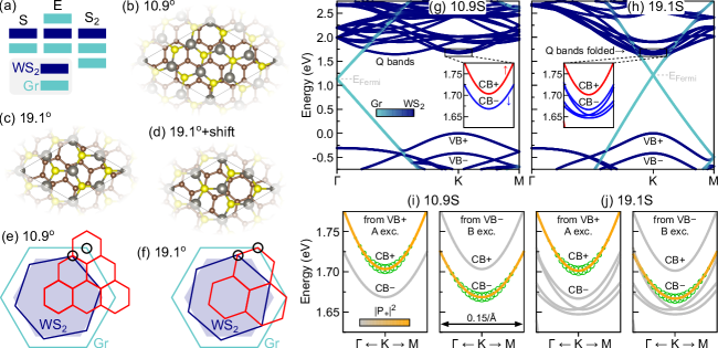
In Fig. 2(a), we depict the TMD/Gr systems considered here and contemplate three different cases: graphene as a substrate (S), graphene encapsulation (E) and bilayer graphene as a substrate (S). The S and E cases are chosen to mimic the Gr/WS2 and the Gr/WS2/Gr experimental samples discussed in Section II. The S2 configuration has no experimental counterpart in this study, but it is a typical structure considered by the Gr community as a platform for proximity-induced SOC effects[80, 81, 82, 83]. In Fig. 2(b-d), we show the atomic structures of the WS2/Gr supercells for the different twist angles considered in this study, i.e., 10.9∘ in Fig. 2(b), 19.1∘ in Fig. 2(c) and 19.1∘ with an in-plane shift in Fig. 2(d). The encapsulated systems have an additional graphene layer on top of the TMD while the bilayer graphene cases have a second graphene layer below, either with AB (Bernal) or AA stacking. Particularly, these two twist angles we consider here (10.9∘ and 19.1∘) provide a relatively small number of atoms (see Supplemental Note V[66]) and different folding of points (see next paragraph).
In the reciprocal space, the twist angle defines how different points of the individual layers are mapped, or folded, to the reciprocal space of the supercell. The first Brillouin zone (BZ) of Gr, WS2 and the resulting supercell are shown in Figs. 2(e,f) for 10.9∘ and 19.1∘, respectively. Importantly, the relative alignment of the points in TMD and Gr happen at different positions for the two different angles, thus serving as the limiting cases for our analysis of the interlayer coupling effect. In realistic systems with long moiré lengths in real space (10s of nm), many more BZs of the supercell would fit in the TMD and Gr BZs and therefore many more points of the individual layers would be folded to a single point of the supercell BZ.
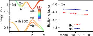
The folding of the different points, as well as the interactions between the layers, can be directly seen in the electronic properties (akin to electronic levels interacting via weak periodic potentials[84]). In Figs. 2(g,h) we show the layer-resolved band structures for 10.9S and 19.1S cases, respectively. It is evident that these two choices of twist angle provide different alignments between the low energy TMD bands and the Dirac cone, i.e., for 10.9∘ (19.1∘) the TMD bands are located at the point and the Dirac cone is located at the () point, in agreement with the expectations from Figs. 2(e,f). Furthermore, besides the folding of points, the interlayer coupling between WS2 and Gr induces splittings to the energy bands, more visible in the regions where dark and bright blue regions overlap. The valence bands are nicely isolated from the other bands, whereas the conduction bands (indicated by the black rectangles, expanded as the inset) show a different behavior, particularly, the folding of the point conduction bands to the point in the 19.1S case. We highlight the spin orientation of these folded bands in the inset and they exhibit the same spin direction as in the .
In Figs. 2(i,j) we focus on the energy scale of the conduction bands that are contained in the insets in Figs. 2(g,h). The color code, from gray to orange, indicates the amplitude of the dipole transition from the with circularly polarized light, in order to identify the optical transitions that contribute to . Our calculations show that the selection rules still hold in the heterostructure and, more importantly, that the point folded bands are optically inactive. The exciton spreading in -space is also shown (using the calculated values of the Gr/WS2 case, discussed in Section II with details in Supplemental Note IV[66]) and reveals that only a small region around the point is relevant, in line with robust GW-BSE calculations in bare monolayers[85]. Therefore, we can investigate the signatures of the WS2/Gr hybridization by simply computing the -factors of and directly at the points of the heterostructure.
In order to investigate the modified valley Zeeman physics due to the microscopic effects of WS2/Gr interlayer hybridization and its signature on the experimentally observed exciton -factors (given in Eq. 3), we must evaluate the Zeeman shift of the Bloch band (generally identified by the index and crystal momentum ):
| (4) | |||||
where is the external magnetic field (in the out-of-plane direction, , as in Fig. 1(a), and , and are the orbital angular momenta, spin angular momenta and -factor of the Bloch band, respectively. The calculation of the orbital angular momentum in the out-of-plane direction, for a Bloch state is obtained via the summation-over-bands approach[43, 86, 39, 40, 41, 42, 46]
| (5) |
in which (), with being the momentum operator, and the spin angular momentum is calculated as
| (6) |
with the Pauli matrix acting on the spin-up and spin-down states of the spinorial Bloch state. We note that, because of time-reversal symmetry, the relation holds for . For further details on this theoretical approach applied to TMDs, we refer to Refs.[39, 40, 41, 42, 46].
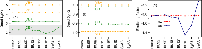
The calculated orbital and spin angular momenta of the and bands are shown in Figs. 3(a,b), respectively, for the investigated WS2/Gr heterostructures. Our results reveal that of , highlighted by the gray area in Fig. 3(a), is distinctly modified, either increasing or decreasing with respect to the monolayer value depending on the particular system. The orbital angular momenta of the remaining bands ( and ) barely changes. Additionally, we have not observed any changes in the spin angular momenta of the investigated bands. Combining the and of the energy bands, we can evaluate the A and B exciton g-factors via Eq. 3. The calculated values of and are shown in Fig. 3(c). While is essentially constant, is visibly changing (due to of ), revealing that there are indeed sizable contributions to the valley Zeeman of excitons arising from the interlayer coupling between WS2 and Gr layers. Therefore, we attribute the experimentally observed changes of (Table 1) to manifestations of the interlayer hybridization at the Gr/WS2 interface. We note that the monolayer thickness is slightly modified when we perform the atomic relaxation of the heterostructure, but this effect is not responsible for the drastic changes in (see Supplemental Note V[66] for this comparison). Furthermore, we emphasize that our numerical calculations for are fully converged with respect to the number of bands (see in Supplemental Note V[66] the comparison of monolayer and the 19.1E case).
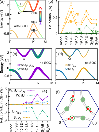
At a first glance, it may seem counter intuitive that the largest change of the -factor originates from the orbital degree of freedom of the conduction band . In Fig. 4(a) we show the wave function localization in the W and S atomic spheres for pristine WS2 monolayer including SOC. The conduction bands, , at the point are highly localized at the W atoms, while valence bands, , are more delocalized across the layer towards the S atoms. Since bands are more delocalized, one might expect them to be be more sensitive to the effect of the adjacent layers. In fact, the percentage of the wave function that “leaks” to the Gr layer is larger for bands, as shown in Fig. 4(b). Nevertheless, the largest changes to the band -factors are observed for , as shown in Fig. 3(a). Interestingly, the spin degree of freedom of band in W-based TMDs is also the most affected by strain[46].
We now turn to the central aspect of our theoretical analysis, i. e., the microscopic mechanism behind the changes in of . For this purpose, we performed a detailed investigation of the orbital composition of the low energy bands and . The monolayer WS2 is summarized in Fig. 4(c,d) (SOC is neglected to simplify the visualization) and gives us the base values to compare with the investigated heterostructures. The conduction (valence) bands at the point are dominated by d (d) atomic orbitals of the W atom[67] while conduction bands at the point are mainly composed of d orbitals of the W atom. The p-like orbitals of the S atoms also provide a visible contribution, particular for the valence band at the point and conduction bands at the point. In Fig. 4(e) we present the contribution of d-like (p-like) orbitals in W (S) atoms of the band for the different WS2/Gr systems, considering the monolayer case as reference. Surprisingly, we observe a decrease of the d character of the W atom, accompanied with an increase of the d character of the W atom and p-like character (p and p) of the S atoms, consistent with the orbital signature of the conduction band at the point. The full orbital decomposition analysis is shown in the Supplemental Note VI[66]. For the 19.1∘ cases, besides the folding of the bands to the point, these bands also have a strong coupling to the Gr Dirac cone, as shown in Fig. 4(f) for the first-order Umklapp condition[87, 22, 23], thus mediating the coupling between and Gr states. We can summarize the hybridization mechanism as following: the TMD conduction bands at the points (more delocalized than point bands) strongly couple with the Dirac cone in Gr (which has a large magnetic moment[88]) and then hybridize with the TMD conduction bands at the point. Because of the nearly resonant condition [horizontal dashed line in Fig. 4(a)] and spin selectivity of folded bands and bands [inset in Fig. 2(h)], the orbital angular momentum of can be strongly altered and thus the valley Zeeman physics of the B exciton is more susceptible to changes. These unexpected proximity effects in the conduction bands of TMDs are also present in other van der Waals heterostructures. For instance, in TMDs coupled to ferromagnetic materials[89, 90, 91, 92, 93], the proximity-induced exchange splitting is also quite complex and can be stronger in the conduction band depending on the particular geometry and stacking of the heterostructure.
We emphasize that the orbital angular momentum is not evaluated locally in the atomic spheres, but takes into account the whole spread of the wave function in the heterostructure, embedded in the transition matrix elements that enter the summation-over-bands expression of in Eq. 5. The orbital decomposition analysis in Fig. 4 and Supplemental Note VI[66] provides a compact way of visualising the spreading of the wave function throughout the system and which bands from the original Gr and TMD layer are hybridizing in the heterostructure. In terms of perturbative approaches and effective models, the orbital decomposition analysis extracted from DFT provides valuable microscopic insight on the type of perturbation order and coupling mechanism behind the observed effects (such as changes in or ). For instance, a direct contribution of Gr states would encode some type of first order coupling, whereas the modification of the orbital decomposition within the TMD would encode higher order processes (virtual interlayer tunneling[23, 25]). It is beyond the scope of this study to provide a full account of this physical phenomena in terms of effective models, such as performed in Refs.[22, 23, 25], but, instead, reveal the underlying microscopic picture within DFT, similarly to Refs.[24, 26].
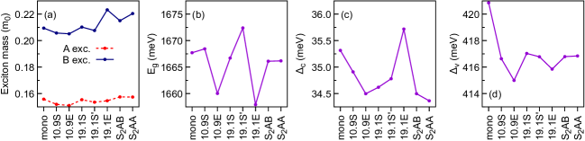
We have also analyzed the reduced exciton masses extracted directly from the DFT calculations, presented in Fig. 5(a), and found that the reduced mass for the A exciton barely changes while for the B exciton the reduced mass changes , which are still rather weak to be clearly visible in experiments[30]. Moreover, we inspected the variations in the relevant energy scales , and [defined in Fig. 1(b)]. We found that the band gap varies by meV, varies meV and varies meV for the different systems, which are relatively small changes. The associated correction to the -factor due to variations in is on the order of , certainly smaller than the observed changes in Fig. 3. These small contributions originating from the energy parameters provide further support to our picture that changes in are indeed manifestations of the complex nature of wave function hybridization across the different layers in the van der Waals heterostructure[4, 5, 6]. Finally, we note that effective masses and transition matrix elements are essentially unaffected over the different WS2/Gr systems investigated[see Figs. 2(i,j) and Fig. 5(a)], providing further support to the perspective that Gr alters the exciton binding energies on the dielectric level[94, 33, 31] (see also discussions in Section II and Supplemental Note III[66]).
With this microscopic understanding, it would be interesting to consider a limiting scenario in which the modification of the valley Zeeman physics mediated by the point folded bands is essentially suppressed, thus isolating the direct contribution of Gr. Unlike monolayer WS2, shown in Fig. 3(a-c), in Mo-based TMD monolayers the point conduction bands above the valleys[95, 96] and therefore we expect this resonant coupling to be strongly suppressed in MoX2/Gr (X=S,Se) systems. In order to verify this hypothesis and strengthen our understanding discussed above, we have analyzed the 10.9S and 19.1S cases for MoS2/Gr heterostructures and summarize our findings in Fig. 6 (with further details given in Supplemental Note VIII[66]). Because the bands (either or ) are energetically out-of-resonance with respect to the bands [Fig. 6(a)], we found no significant changes to the exciton -factors when comparing the monolayer with the 10.9S and 19.1S MoS2/Gr heterostructures, shown in Fig. 6(b), in line with our understanding that point bands are crucial to mediate the interaction between Dirac cone of Gr and the point bands of the TMD.
IV. Modified valley Zeeman physics by graphene as a dielectric
To complete our analysis, we investigate the modification of the valley Zeeman physics of WS2 monolayer due to the influence of Gr on the dielectric level, motivated by the fact that the binding energy, , and the exciton emission energy can be well explained in terms of dielectric screening effects[94, 33, 31] (see also Section II and Supplemental Note III[66]). There are two relevant effects related to the influence of the dielectric screening on the exciton emission energy: (i) the band gap reduction (rigid band shift)[97, 31], which is eV[33] in the Gr/WS2 (Gr/WS2/Gr) case; and (ii) the localization of the exciton wave function in -space (increase of the exciton radius in real space), which can be directly extracted from our calculations (see Table III in Supplemental Note IV[66] for the changes in the FWHM of the exciton envelope function). We note that recent experiments have shown that the measured band and exciton -factors agree remarkably well with density functional theory (DFT) calculations without excitonic corrections[98, 99]. However, it is in principle expected that excitonic effects renormalize the exciton -factors by averaging the spin and orbital degrees of freedom around the valleys[40, 100, 101, 102, 103, 104]. In order to provide a cohesive and comprehensive picture of the valley Zeeman physics, we explore the consequences of the band gap reduction and wave function localization by considering a pristine monolayer WS2 (with a lattice parameter of 3.153 Å and thickness of 3.14 Å[95], without any relaxation from the heterostructure). The DFT calculations provide the fundamental information for the -factors and effective masses of the low-energy bands (see Fig. 1(b) for the relevant bands). The exciton wave functions are calculated within the effective Bethe-Salpeter equation in -space using the DFT effective masses as input (details in Supplemental Note IV[66]). The computational details for the DFT calculations can be found in the Supplemental Note V[66].
The band gap reduction due to the increased dielectric screening can be taken into account by applying a scissor shift to the calculated DFT band gap, i. e., a negative rigid energy shift to all conduction bands. These shifts are then incorporated in the energy differences that appear in the expression for the orbital angular momentum in Eq. 5. In Table 2, we present the calculated exciton -factors for scissor shifts of , and eV. The -factors and become more negative as we decrease the band gap by eV. On the other hand, the difference is rather small () and barely changes with the applied scissor shift. Therefore, the reduced band gap due to increased dielectric screening in WS2/Gr heterostructures is unlikely to drastically modify the quantity . We point out that our calculated -factors given in Table 2 are in excellent agreement with the experimental values given Table 1 for the WS2 case, which is consistent with the previous reports comparing DFT-based calculations with experimentally determined band and exciton -factors in WSe2[98] and WS2[99].
| Scissor shift (eV) | |||
|---|---|---|---|
| WS2 | Gr/WS2 | Gr/WS2/Gr | ||
|---|---|---|---|---|
| DFT | ||||
| mass | ||||
| Corr. | ||||
| mass | ||||
The effect of the dielectric screening on the spatial extension of the exciton wave function and how it translates to the exciton -factor can be investigated by the following relation[40, 102, 103]
| (7) |
in which is the exciton state generated by the conduction band, , and valence band, , described by the envelope function , with wave vector centered at the valley. Since the 1s exciton envelope function in our approximation has a radial symmetry, we also consider such dependence for the -factors, as discussed in Supplemental Note IX[66]. We summarize our results in Table 3. The absolute values of both and become less negative, providing a worse comparison with experiments (considering the WS2 case as reference, shown in Table 1), but consistent with the renormalization effects observed in previous theoretical works[100, 40]. More importantly, the difference remains quite small and barely changes with the increased dielectric confinement. Furthermore, the calculated values of and are consistent whether we use the DFT masses or the corrected values (increased by to approach experimental values[32]). Interestingly, the calculated g-factor change from the WS2 to the Gr/WS2/Gr case is 0.25 (0.29) for the A (B) excitons, which is in line with the experimental value of 0.29 (0.33). Our analysis suggest that the observed changes in do not originate from the dielectric effect on the exciton wave function.
Besides the dielectric effects, it is also worth mentioning the possible role of strain that could be present in the WS2/Gr heterostructures due to the growth process. Typically, the reminiscent strain from the fabrication procedure was be estimated to be on the order of [105, 106]. Furthermore, recent calculations[46] have shown that in monolayer TMDs, and do not deviate from each other unless there is a sizable amount of compressive strain 2%, leading to , which is accompanied with a reduction of the magnitude in both g-factors, i. e., and become less negative. This level of strain is very unlikely to be present in our samples, as this would be easily noticeable in the exciton energy (shifts due to strain are typically on the order of 100 meV/%)[96, 107].
We wrap up our theoretical analysis by emphasizing that the calculated dielectric effects of band gap reduction and exciton wave function localization are able to explain the monotonic behavior of the observed -factors (they become more negative as the dielectric confinement increases). On the other hand, the drastic changes observed in (from negative to positive) can only be explained by our first principles calculations (Section III) including the microscopic effect of the interlayer coupling between WS2 and graphene, which ultimately translates to changes in originating from the orbital degree of freedom of the lower conduction band .
V. Concluding remarks
In summary, we reveal signatures of proximity-enhanced valley Zeeman physics, detected through high field magneto optical spectroscopy on the A- and B-exciton of Gr-encapsulated ML WS2. We investigate the markedly different evolution of the and -factors through first principles calculations by exploring different prototypical scenarios of the twist angle, stacking and material composition. We reveal that the proximity effect due to the Gr-encapsulation mainly appears in the lowest -point CB of WS2 () due to the modification of the orbital angular momentum, while the spin angular momentum is nearly unaffected. We reveal a mechanism, where the hybridization of the CB -point with is mediated by the Gr Dirac cone and enhanced through commensurate stacking and the energetic alignment of the conduction bands at the - and -point.
We expect our results to be general for van der Waals and moiré heterostructures, also affecting spin dynamics at such interfaces. Particularly, we show how sensitive the -factor is to the detailed nuances of the wave function hybridization, ultimately translated to the orbital degree of freedom in a non-intuitive manner. We therefore expand the concept of proximity effects in these heterostructures and show how magnetooptical experiments combined with first principles calculations can be used as a tool to quantify wave function hybridization. Future work may exploit the possibility to resonantly tune the coupling across layers via external electric fields, long-range moiré scales and mechanical deformations.
References
- [1] Geim A K and Grigorieva I V 2013 Nature 499 419
- [2] Song J C W and Gabor N M 2018 Nature Nanotechnology 13 986
- [3] Sierra J F, Fabian J, Kawakami R K, Roche S and Valenzuela S O 2021 Nature Nanotechnology 16 856
- [4] Slobodkin Y, Mazuz-Harpaz Y, Refaely-Abramson S, Gazit S, Steinberg H and Rapaport R 2020 Physical Review Letters 125 255301
- [5] Plankl M, Faria Junior P E, Mooshammer F, Siday T, Zizlsperger M, Sandner F, Schiegl F, Maier S, Huber M A, Gmitra M, Fabian J, Boland J L, Cocker T L and Huber R 2021 Nature Photonics 15 594
- [6] Barré E, Karni O, Liu E, O’Beirne A L, Chen X, Ribeiro H B, Yu L, Kim B, Watanabe K, Taniguchi T, Barmak K, Lui C H, Refaely-Abramson S, da Jornada F H and Heinz T F 2022 Science 376 406
- [7] Žutić I, Matos-Abiague A, Scharf B, Dery H and Belashchenko K 2019 Materials Today 22 85
- [8] Castro Neto A H, Guinea F, Peres N M R, Novoselov K S and Geim A K 2009 Reviews of Modern Physics 81 109
- [9] Avsar A, Ochoa H, Guinea F, Özyilmaz B, van Wees B J and Vera-Marun I J 2020 Reviews of Modern Physics 92 021003
- [10] Avsar A, Tan J Y, Taychatanapat T, Balakrishnan J, Koon G K W, Yeo Y, Lahiri J, Carvalho A, Rodin A S, O’Farrell E C T, Eda G, Castro Neto A H and Özyilmaz B 2014 Nature Communications 5 4875
- [11] Gmitra M and Fabian J 2015 Physical Review B 92 155403
- [12] Gmitra M, Kochan D, Högl P and Fabian J 2016 Physical Review B 93 155104
- [13] Avsar A, Unuchek D, Liu J, Sanchez O L, Watanabe K, Taniguchi T, Ozyilmaz B and Kis A 2017 ACS Nano 11 11678
- [14] Luo Y K, Xu J, Zhu T, Wu G, McCormick E J, Zhan W, Neupane M R and Kawakami R K 2017 Nano Letters 17 3877
- [15] Cummings A W, Garcia J H, Fabian J and Roche S 2017 Physical Review Letters 119 206601
- [16] Fülöp B, Márffy A, Zihlmann S, Gmitra M, Tóvári E, Szentpéteri B, Kedves M, Watanabe K, Taniguchi T, Fabian J et al. 2021 npj 2D Materials and Applications 5 82
- [17] Ojeda-Aristizabal C, Ferrier M, Guéron S and Bouchiat H 2009 Physical Review B 79 165436
- [18] Natterer F D, Ha J, Baek H, Zhang D, Cullen W G, Zhitenev N B, Kuk Y and Stroscio J A 2016 Physical Review B 93 045406
- [19] Burset P, Yeyati A L and Martín-Rodero A 2008 Physical Review B 77 205425
- [20] Högl P, Frank T, Kochan D, Gmitra M and Fabian J 2020 Physical Review B 101 245441
- [21] Frank T, Högl P, Gmitra M, Kochan D and Fabian J 2018 Physical Review Letters 120 156402
- [22] Li Y and Koshino M 2019 Physical Review B 99 075438
- [23] David A, Rakyta P, Kormányos A and Burkard G 2019 Physical Review B 100 085412
- [24] Naimer T, Zollner K, Gmitra M and Fabian J 2021 Physical Review B 104 195156
- [25] Péterfalvi C G, David A, Rakyta P, Burkard G and Kormányos A 2022 Physical Review Reserarch 4 L022049
- [26] Pezo A, Zanolli Z, Wittemeier N, Ordejón P, Fazzio A, Roche S and Garcia J H 2021 2D Materials 9 015008
- [27] Stier A V, McCreary K M, Jonker B T, Kono J and Crooker S A 2016 Journal of Vacuum Science & Technology B 34 04J102
- [28] Wierzbowski J, Klein J, Sigger F, Straubinger C, Kremser M, Taniguchi T, Watanabe K, Wurstbauer U, Holleitner A W, Kaniber M, Müller K and Finley J J 2017 Scientific Reports 7 12383
- [29] Cadiz F, Courtade E, Robert C, Wang G, Shen Y, Cai H, Taniguchi T, Watanabe K, Carrere H, Lagarde D, Manca M, Amand T, Renucci P, Tongay S, Marie X and Urbaszek B 2017 Physical Review X 7 021026
- [30] Raja A, Waldecker L, Zipfel J, Cho Y, Brem S, Ziegler J D, Kulig M, Taniguchi T, Watanabe K, Malic E, Heinz T F, Berkelbach T C and Chernikov A 2019 Nature Nanotechnology 14 832
- [31] Waldecker L, Raja A, Rösner M, Steinke C, Bostwick A, Koch R J, Jozwiak C, Taniguchi T, Watanabe K, Rotenberg E, Wehling T O and Heinz T F 2019 Physical Review Letters 123 206403
- [32] Goryca M, Li J, Stier A V, Taniguchi T, Watanabe K, Courtade E, Shree S, Robert C, Urbaszek B, Marie X and Crooker S A 2019 Nature Communications 10 4172
- [33] Raja A, Chaves A, Yu J, Arefe G, Hill H M, Rigosi A F, Berkelbach T C, Nagler P, Schüller C, Korn T, Nuckolls C, Hone J, Brus L E, Heinz T F, Reichman D R and Chernikov A 2017 Nature Communications 8 15251
- [34] Lorchat E, López L E P, Robert C, Lagarde D, Froehlicher G, Taniguchi T, Watanabe K, Marie X and Berciaud S 2020 Nature Nanotechnology 15 283
- [35] Tebbe D, Schütte M, Watanabe K, Taniguchi T, Stampfer C, Beschoten B and Waldecker L 2022 arXiv:2212.00118
- [36] Enderlein R and Horing N J M 1997 Fundamentals of semiconductor physics and devices (Singapore: World Scientific)
- [37] Yu P Y and Cardona M 2001 Fundamentals of semiconductors: physics and materials properties (Berlin: Springer)
- [38] Winkler R 2003 Spin-orbit coupling effects in two-dimensional electron and hole systems vol 191 (Springer)
- [39] Woźniak T, Faria Junior P E, Seifert G, Chaves A and Kunstmann J 2020 Physical Review B 101 235408
- [40] Deilmann T, Krüger P and Rohlfing M 2020 Physical Review Letters 124 226402
- [41] Förste J, Tepliakov N V, Kruchinin S Y, Lindlau J, Funk V, Förg M, Watanabe K, Taniguchi T, Baimuratov A S and Högele A 2020 Nature Communications 11 4539
- [42] Xuan F and Quek S Y 2020 Physical Review Research 2 033256
- [43] Roth L M, Lax B and Zwerdling S 1959 Physical Review 114 90
- [44] Covre F S, Faria Junior P E, Gordo V O, de Brito C S, Zhumagulov Y V, Teodoro M D, Couto O D D, Misoguti L, Pratavieira S, Andrade M B, Christianen P C M, Fabian J, Withers F and Galvão Gobato Y 2022 Nanoscale 14 5758
- [45] Blundo E, Faria Junior P E, Surrente A, Pettinari G, Prosnikov M A, Olkowska-Pucko K, Zollner K, Woźniak T, Chaves A, Kazimierczuk T, Felici M, Babiński A, Molas M R, Christianen P C M, Fabian J and Polimeni A 2022 Physical Review Letters 129 067402
- [46] Faria Junior P E, Zollner K, Woźniak T, Kurpas M, Gmitra M and Fabian J 2022 New Journal of Physics 24 083004
- [47] Gillen R 2021 physica status solidi (b) 258 2000614
- [48] Förg M, Baimuratov A S, Kruchinin S Y, Vovk I A, Scherzer J, Förste J, Funk V, Watanabe K, Taniguchi T and Högele A 2021 Nature communications 12 1656
- [49] Heißenbüttel M C, Deilmann T, Krüger P and Rohlfing M 2021 Nano Letters 21 5173
- [50] Zhao S, Huang X, Li Z, Rupp A, Göser J, Vovk I A, Kruchinin S Y, Watanabe K, Taniguchi T, Bilgin I et al. 2022 arXiv:2202.11139
- [51] Kipczak Ł, Slobodeniuk A O, Woźniak T, Bhatnagar M, Zawadzka N, Olkowska-Pucko K, Grzeszczyk M, Watanabe K, Taniguchi T, Babiński A and Molas M R 2022 arXiv:2211.16186
- [52] Arora A, Schmidt R, Schneider R, Molas M R, Breslavetz I, Potemski M and Bratschitsch R 2016 Nano Letters 16 3624
- [53] Roch J G, Froehlicher G, Leisgang N, Makk P, Watanabe K, Taniguchi T and Warburton R J 2019 Nature Nanotechnology 14 432
- [54] Roch J G, Miserev D, Froehlicher G, Leisgang N, Sponfeldner L, Watanabe K, Taniguchi T, Klinovaja J, Loss D and Warburton R J 2020 Physical Review Letters 124 187602
- [55] Klein J, Hötger A, Florian M, Steinhoff A, Delhomme A, Taniguchi T, Watanabe K, Jahnke F, Holleitner A W, Potemski M, Faugeras C, Finley J J and Stier A V 2021 Physical Review Research 3 L022009
- [56] Klein J, Florian M, Hötger A, Steinhoff A, Delhomme A, Taniguchi T, Watanabe K, Jahnke F, Holleitner A W, Potemski M, Faugeras C, Stier A V and Finley J J 2022 Physical Review B 105 L041302
- [57] Grzeszczyk M, Olkowska-Pucko K, Nogajewski K, Watanabe K, Taniguchi T, Kossacki P, Babiński A and Molas M R 2021 Nanoscale 13 18726
- [58] Li W, Lu X, Wu J and Srivastava A 2021 Nature Nanotechnology 16 148
- [59] Raiber S, Faria Junior P E, Falter D, Feldl S, Marzena P, Watanabe K, Taniguchi T, Fabian J and Schüller C 2022 Nature Communications 13 4997
- [60] McCreary K M, Hanbicki A T, Robinson J T, Cobas E, Culbertson J C, Friedman A L, Jernigan G G and Jonker B T 2014 Advanced Functional Materials 24 6449
- [61] McCreary K M, Hanbicki A T, Jernigan G G, Culbertson J C and Jonker B T 2016 Scientific Reports 6 19159
- [62] Paradisanos I, McCreary K M, Adinehloo D, Mouchliadis L, Robinson J T, Chuang H J, Hanbicki A T, Perebeinos V, Jonker B T, Stratakis E and Kioseoglou G 2020 Applied Physics Letters 116 203102
- [63] McCreary K M, Hanbicki A T, Singh S, Kawakami R K, Jernigan G G, Ishigami M, Ng A, Brintlinger T H, Stroud R M and Jonker B T 2016 Scientific Reports 6 35154
- [64] McCreary K M, Hanbicki A T, Sivaram S V and Jonker B T 2018 APL Materials 6 111106
- [65] Stier A V, McCreary K M, Jonker B T, Kono J and Crooker S A 2016 Nature Communications 7 10643
- [66] See Supplemental Material at [link] for details on the (I) experimental setup, (II) dielectric screening in 2D materials stacks, (III) determining the exciton binding energy from high field diamagnetic shift, (IV) calculation of the exciton binding energies and wavefunctions, (V) details on the first-principles calculations, (VI) details on the orbital decomposition, (VII) effect of lattice relaxation, (VIII) the MoS2/Gr systems considered and (IX) excitonic effects on g-factors.
- [67] Xiao D, Liu G B, Feng W, Xu X and Yao W 2012 Physical Review Letters 108
- [68] Chernikov A, van der Zande A M, Hill H M, Rigosi A F, Velauthapillai A, Hone J and Heinz T F 2015 Physical Review Letters 115 126802
- [69] Blaha P, Schwarz K, Tran F, Laskowski R, Madsen G K and Marks L D 2020 The Journal of Chemical Physics 152 074101
- [70] Lejaeghere K, Bihlmayer G, Björkman T, Blaha P, Blügel S, Blum V, Caliste D, Castelli I E, Clark S J, Corso A D, de Gironcoli S, Deutsch T, Dewhurst J K, Marco I D, Draxl C, Dułak M, Eriksson O, Flores-Livas J A, Garrity K F, Genovese L, Giannozzi P, Giantomassi M, Goedecker S, Gonze X, Grånäs O, Gross E K U, Gulans A, Gygi F, Hamann D R, Hasnip P J, Holzwarth N A W, Iuşan D, Jochym D B, Jollet F, Jones D, Kresse G, Koepernik K, Küçükbenli E, Kvashnin Y O, Locht I L M, Lubeck S, Marsman M, Marzari N, Nitzsche U, Nordström L, Ozaki T, Paulatto L, Pickard C J, Poelmans W, Probert M I J, Refson K, Richter M, Rignanese G M, Saha S, Scheffler M, Schlipf M, Schwarz K, Sharma S, Tavazza F, Thunström P, Tkatchenko A, Torrent M, Vanderbilt D, van Setten M J, Speybroeck V V, Wills J M, Yates J R, Zhang G X and Cottenier S 2016 Science 351
- [71] Gmitra M, Konschuh S, Ertler C, Ambrosch-Draxl C and Fabian J 2009 Physical Review B 80 235431
- [72] Konschuh S, Gmitra M and Fabian J 2010 Physical Review B 82 245412
- [73] Kurpas M, Gmitra M and Fabian J 2016 Physical Review B 94 155423
- [74] Kurpas M, Faria Junior P E, Gmitra M and Fabian J 2019 Physical Review B 100 125422
- [75] Faria Junior P E, Kurpas M, Gmitra M and Fabian J 2019 Physical Review B 100 115203
- [76] Ratha S, Simbeck A J, Late D J, Nayak S K and Rout C S 2014 Applied Physics Letters 105 243502
- [77] Paradisanos I, McCreary K M, Adinehloo D, Mouchliadis L, Robinson J T, Chuang H J, Hanbicki A T, Perebeinos V, Jonker B T, Stratakis E and Kioseoglou G 2020 Applied Physics Letters 116 203102
- [78] Yang C H and Chang S T 2022 Photonics 9 387
- [79] Choi S M, Jhi S H and Son Y W 2010 Physical Review B 81 081407
- [80] Gmitra M and Fabian J 2017 Physical Review Letters 119 146401
- [81] Lee Y, Knothe A, Overweg H, Eich M, Gold C, Kurzmann A, Klasovika V, Taniguchi T, Wantanabe K, Fal’ko V, Ihn T, Ensslin K and Rickhaus P 2020 Physical Review Letters 124 126802
- [82] Amann J, Völkl T, Rockinger T, Kochan D, Watanabe K, Taniguchi T, Fabian J, Weiss D and Eroms J 2022 Physical Review B 105 115425
- [83] Zhang Y, Polski R, Thomson A, Lantagne-Hurtubise É, Lewandowski C, Zhou H, Watanabe K, Taniguchi T, Alicea J and Nadj-Perge S 2023 Nature 613 268
- [84] Ashcroft N W and Mermin N D 1976 Solid state physics (Harcourt: Brooks Cole)
- [85] Katznelson S, Cohn B, Sufrin S, Amit T, Mukherjee S, Kleiner V, Mohapatra P, Patsha A, Ismach A, Refaely-Abramson S, Hasman E and Koren E 2022 Materials Horizons 9 1089
- [86] Chang M C and Niu Q 1996 Physical Review B 53 7010
- [87] Koshino M 2015 New Journal of Physics 17 015014
- [88] Frank T and Fabian J 2020 Physical Review B 102 165416
- [89] Zollner K, Faria Junior P E and Fabian J 2019 Physical Review B 100 085128
- [90] Zollner K, Faria Junior P E and Fabian J 2020 Physical Review B 101 085112
- [91] Ge M, Wang H, Wu J, Si C, Zhang J and Zhang S 2022 npj Computational Materials 8
- [92] Zollner K, Faria Junior P E and Fabian J 2023 Physical Review B 107 035112
- [93] Choi J, Lane C, Zhu J X and Crooker S A 2022 Nature Materials
- [94] Stier A V, Wilson N P, Clark G, Xu X and Crooker S A 2016 Nano Letters 16 7054
- [95] Kormányos A, Burkard G, Gmitra M, Fabian J, Zólyomi V, Drummond N D and Fal’ko V 2015 2D Materials 2 022001
- [96] Zollner K, Faria Junior P E and Fabian J 2019 Physical Review B 100 195126
- [97] Cho Y and Berkelbach T C 2018 Physical Review B 97 041409
- [98] Robert C, Dery H, Ren L, Van Tuan D, Courtade E, Yang M, Urbaszek B, Lagarde D, Watanabe K, Taniguchi T, Amand T and Marie X 2021 Physical Review Letters 126 067403
- [99] Zinkiewicz M, Woźniak T, Kazimierczuk T, Kapuscinski P, Oreszczuk K, Grzeszczyk M, Bartoš M, Nogajewski K, Watanabe K, Taniguchi T, Faugeras C, Kossacki P, Potemski M, Babiński A and Molas M R 2021 Nano Letters 21 2519
- [100] Chen S Y, Lu Z, Goldstein T, Tong J, Chaves A, Kunstmann J, Cavalcante L S R, Woźniak T, Seifert G, Reichman D R, Taniguchi T, Watanabe K, Smirnov D and Yan J 2019 Nano Letters 19 2464
- [101] Gillen R 2021 physica status solidi (b) 258 2000614
- [102] Heißenbüttel M C, Deilmann T, Krüger P and Rohlfing M 2021 Nano Letters 21 5173
- [103] Amit T, Hernangómez-Pérez D, Cohen G, Qiu D Y and Refaely-Abramson S 2022 Physical Review B 106 L161407
- [104] Hötger A, Amit T, Klein J, Barthelmi K, Pelini T, Delhomme A, Rey S, Potemski M, Faugeras C, Cohen G, Hernangómez-Pérez D, Taniguchi T, Watanabe K, Kastl C, Finley J J, Refaely-Abramson S, Holleitner A W and Stier A V 2022 arXiv:2205.10286
- [105] Mennel L, Furchi M M, Wachter S, Paur M, Polyushkin D K and Mueller T 2018 Nature Communications 9 516
- [106] Darlington T P, Carmesin C, Florian M, Yanev E, Ajayi O, Ardelean J, Rhodes D A, Ghiotto A, Krayev A, Watanabe K, Taniguchi T, Kysar J W, Pasupathy A N, Hone J C, Jahnke F, Borys N J and Schuck P J 2020 Nature Nanotechnology 15 854
- [107] Frisenda R, Drüppel M, Schmidt R, Michaelis de Vasconcellos S, Perez de Lara D, Bratschitsch R, Rohlfing M and Castellanos-Gomez A 2017 npj 2D Materials and Applications 1 10