Observation of highly anisotropic bulk dispersion and spin-polarized topological surface states in CoTe2
Abstract
We present CoTe2 as a new type-II Dirac semimetal supporting Lorentz symmetry violating Dirac fermions in the vicinity of the Fermi energy. By combining first principle ab-initio calculations with experimental angle-resolved photo-emission spectroscopy results, we show the CoTe2 hosts a pair of type-II Dirac fermions around 90 meV above the Fermi energy. In addition to the bulk Dirac fermions, we find several topological band inversions in bulk CoTe2, which gives rise to a ladder of spin-polarized surface states over a wide range of energies. In contrast to the surface states which typically display Rashba type in-plane spin splitting, we find that CoTe2 hosts novel out-of-plane spin polarization as well. Our work establishes CoTe2 as a potential candidate for the exploration of Dirac fermiology and applications in spintronic devices, infrared plasmonics, and ultrafast optoelectronics.
I Introduction
The broad class of layered transition metal dichalcogenides (TMDs) has attracted significant attention in the last decades due to their novel electronic, optical, and topological properties, combined with their potential for various applications Yin et al. (2021); Zhang et al. (2020); Fiori et al. (2014); Wang et al. (2016); Chang et al. (2021); Vobornik et al. (2021); D’Olimpio et al. (2022). Owing to the weak inter-layer van der Waals interaction, TMDs offer easy exfoliation of isolated monolayers which host different physical properties from their bulk counterpart. Interesting examples of this include quantum spin Hall effect, superconductivity, charge density wave, and various topological phases Tang et al. (2017); Chen et al. (2018); Liu et al. (2012); Miyata et al. (2015); Chen et al. (2015); Clark et al. (2018a); Noh et al. (2017); Alicea et al. (2011); Chiu et al. (2021); Emmanouilidou et al. (2020); Ghosh et al. (2019); Anemone et al. (2021); Yan et al. (2017); Zhang et al. (2017). The physical and chemical properties of TMDs can be tuned by the selection of the constituents, the crystal structures, and the layer thicknesses Kang et al. (2017); He and Que (2016); Manzeli et al. (2017); Zheng et al. (2016); Mak et al. (2010); Hlevyack et al. (2021); Mukherjee et al. (2020). Specifically, among the TMX2 family of TMDs, PdTe2, PtTe2, PtSe2, and NiTe2 have attracted notable interest due to observation of Lorentz- symmetry violating, type-II Dirac fermions associated with a tilted Dirac cone near the Fermi energy Anemone et al. (2020); Huang et al. (2016); Fei et al. (2017); Clark et al. (2018b); Politano et al. (2018a); Nurmamat et al. (2021); Ghosh et al. (2019); Rizza et al. (2022); Politano et al. (2018b); Xu et al. (2018); Mukherjee et al. (2020); Zhang et al. (2021); Aguilar et al. (2022). The Lorentz-symmetry breaking type-II Dirac fermions have electronic, optical, and other physical properties which are different from those found in other topological semi-metals. The electronic band-structure and spin-polarize topological surface states in these materials have been thoroughly investigated by combining realistic ab-initio calculations with spin-resolved and conventional angle-resolved photoemission spectroscopy (ARPES) experiments.
However, the electronic properties of another prospective candidate material in the series, CoTe2 are yet to be explored 111Zhen Hu1, Libo Zhang, Atasi Chakraborty, Gianluca D’Olimpio, Jun Fujii, Amit Agarwal, Ivana Vobornik, Daniel Farias, Changlong Liu, Chia-Nung Kuo, Chin Shan Lue, Li Han, Kaixuan Zhang, Zhiqingzi Chen, Chenyu Yao, Anping Ge, Yuanchen Zhou, Antonio Politano, Weida Hu, Shao-Wei Wang, Lin Wang, Xiaoshuang Chen and Wei Lu, Terahertz Nonlinear Hall Rectifier Based on Spin-Polarized 1T-CoTe2, To appear in Adv. Mater.. CoTe2 can crystallize in both trigonal () and orthorhombic ( and ) forms. Among these, the centrosymmetric trigonal 1-CoTe2 has recently been shown to be a highly efficient electro-catalyst for water splitting Lu et al. (2015); Chia et al. (2017). In this paper, for the first time, we present a detailed investigation of the electronic structure of 1-CoTe2 by combining first-principles calculations with spin-polarized ARPES experiments. We find that similar to other TMX2 compounds, CoTe2 is also a topological semimetal supporting a type-II Dirac crossing in the vicinity of the Fermi energy. In addition to the bulk electronic structure, we demonstrate that CoTe2 hosts a ladder of topological surface states arising from several topological band inversions in the bulk electronic structure. These give rise to spin-polarized Dirac surface states, with a large spectral weight. We probe this via spin-ARPES measurements and the measured spin-polarized states are consistent with our spin-dependent spectral function calculations. Interestingly, we find that some of the surface states, away from the point, have an out-of-plane spin polarization.
The rest of the paper is organized as follows. We describe the crystal structure and computational details in Sec. II, followed by the details of the spin-ARPES measurements in Sec. III. In Sec. IV, we explore the band structure and geometry of the Fermi surface (FS) in CoTe2. We study the origin of the Dirac states, multiple band inversions, and their origin in CoTe2 employing the ARPES measurement combined with ab initio electronic structure calculations in Sec. V. In Sec. VI, we discuss the spin-polarized surface states and the existence of unique out-of-plane spin-polarized states in CoTe2 calculations. We summarize our findings in Sec. VII.
II Crystal Structure and Theoretical Methods
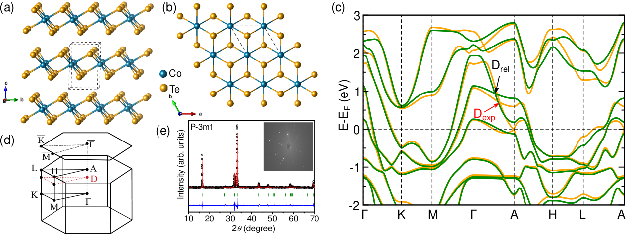
Bulk CoTe2 crystallizes in CdI2-type trigonal structure that belongs to the space group (164). Each unit cell of CoTe2 has one Co atom and two Te atoms. To obtain the minimum-energy structure for CoTe2, we performed the symmetry-protected cell volume and ion relaxation using the conjugate-gradient algorithm until the Hellman-Feynman forces on each atom were less than the tolerance value of 10-4 eV/Å . The cell volume of the experimental structure increased by as a result of the relaxation. The comparison of lattice parameters between experimental and theoretically relaxed structures is presented in Table 1.
| Experimental | Ref 222Topological Quantum Chemistry Database | Relaxed | |
|---|---|---|---|
| a/b (Å) | 3.791(9) | 3.804 | 3.778 |
| c (Å) | 5.417(0) | 5.405 | 5.618 |
The trigonally distorted CoTe6 octahedra accommodating the nearest neighbor Co-Te bonds (Å ) form an edge shared geometrical network on the crystallographic plane [see Fig. 1 (a) and (b)]. Adjacent mono-layers, stacked along the axis, interact via weak Van-der Waals interaction. Fig. 1 (d) shows the corresponding bulk and (001) surface Brillouin zones (BZs) along with the high-symmetry points. The CoTe2 crystal structure possesses threefold rotational symmetry around the -axis (), inversion symmetry , and the three mirror symmetries M100, M010, and M110. Fig. 1 (e) shows the experimental -ray diffraction pattern for CoTe2. The observation of sharp white spots in the Laue diffraction pattern in the inset of Fig. 1 (e) confirms the high quality of the CoTe2 crystals cleaved along the (0001) direction. The presence of the threefold rotation symmetry is also evident.
To perform the ab-initio calculations, we used the density functional theory (DFT) in the plane wave basis set. We used the Perdew-Burke-Ernzerhof (PBE) Perdew et al. (1996) implementation of the generalized gradient approximation (GGA) for the exchange-correlation. This was combined with the projector augmented wave potentials Blöchl (1994); Kresse and Joubert (1999a) as implemented in the Vienna ab initio simulation package (VASP) Kresse and Furthmüller (1996); Kresse and Joubert (1999b). GGA calculations are carried out with and without Coulomb correlation (Hubbard U) and spin-orbit coupling (SOC). The SOC is included in the calculations as a second variational form to the original Hamiltonian. The kinetic energy cutoff of the plane wave basis for the DFT calculations was chosen to be 450 eV. A -centered Monkhorst-Pack Monkhorst and Pack (1976) -point grid was used to perform the momentum-space calculations for the Brillouin zone (BZ) integration of bulk. To calculate the surface spectral function for finite geometry slabs of CoTe2, we construct the tight-binding model Hamiltonian by deploying atom-centered Wannier functions within the VASP2WANNIER90 Marzari and Vanderbilt (1997) codes. Utilizing the obtained tight-binding model, we calculate the surface spectral function using the iterative Green’s function method, as implemented in the WannierTools package Wu et al. (2018).
III ARPES and Spin-ARPES measurements
ARPES and Spin-ARPES measurements were performed at low energy (LE) branch of the APE-NFFA beamline Panaccione et al. (2009) at the Elettra synchrotron facility (Trieste, Italy), which is equipped with VESPA Bigi et al. (2017) as an electron spin polarization detector. The details of the experimental geometry, like the electron analyzer slit opening and incoming photon direction with respect to the analyzer lens axis, can be found in Ref. [Bigi et al., 2017]. To determine the inner potential () of CoTe2 (0001) experimentally, angle-resolved valence band spectra and FS maps were measured for the photon energy range between 13 eV and 85 eV with 2 linear polarizations (- and - polarization). Spin-ARPES maps were acquired for two-photon energies (= 19 eV and 75 eV). The energy and angular resolutions for the Spin-ARPES measurements were set to 100 meV and 1.5∘, respectively. The clean (0001) surface of CoTe2 was obtained by the cleavage of the single crystal in situ in an ultra-high vacuum. The sample temperature during the ARPES and Spin-ARPES measurements was kept at 78 K.
IV Electronic Band-structure and the FS Geometry
The ionic balance of the chemical formula of CoTe2, suggests that the Co and Te atoms are in 3d34s0 and 5s25p6 configurations, respectively. As a consequence, we expect the Co- and Te- orbitals to have a major contribution at the Fermi energy (). We present the bulk band-dispersion in presence of SOC, for the experimental structure, and also for the relaxed structure in Fig. 1(c). The experimental electronic band dispersion in Fig. 1(c), clearly shows the existence of a couple of tilted Dirac-like crossings just above , along the -A high symmetry direction. We find that the position of the Dirac point (DP) is sensitive to small variations of the structural parameters. It shifts from 0.68 eV to 0.92 eV above due to the small change in the structural parameters on relaxation. Since the -A path is an invariant subspace of the three-fold rotational crystal symmetry (), the Dirac cone is protected by the rotational symmetry. This is similar to the Dirac crossing in NiTe2 and other related materials in the same space group Ghosh et al. (2019); Nappini et al. (2020); Rizza et al. (2022). Two accidental linear band crossings, one exactly at on the high symmetry point and another one at 2.2 eV above along the path become gapped due to relaxation, as highlighted in Fig. 1(c).
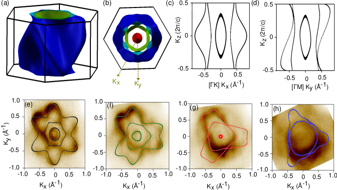
The geometry of the FS and its evolution with change in the Fermi energy is shown in Fig. 2 for the relaxed structure. The 3D FS for is shown in Fig. 2(a). The projection of the FS on a plane perpendicular to the axis in Fig. 2(b) clearly shows three distinct types of band contributions at the FS, each having two-fold degeneracy. Figures 2(c) and (d) capture the projection of the FS on the plane along the line, and the plane along the direction.
The FS along the path is highly anisotropic as seen in Fig. 2(d). Clearly, bulk CoTe2 has a strong momentum-dependent anisotropic FS (see Appendix B for details), which is also expected from the presence of type-II Dirac fermions in the system. To investigate the FS modulations along the direction, we have shown the energy contours at different values in panels (e)-(h) of Fig. 2. The theoretically calculated (solid line) and the experimentally measured (mud color scale) 2D energy contours within the Wigner Seitz cell are shown in Fig. 2(e)-(h) over the plane for different values. Different values are probed in the ARPES experiment by changing the energy of the incident photon beam. Using the free electron final state model Damascelli (2004), we have
| (1) |
Here, is the inner potential, is the kinetic energy of a photoelectron and denotes the emission angled from the sample surface normal. For the different panels of Fig. 2(e)-(h), we have (corresponding ) = 75 eV (0.03 ), 70 eV (0.16 ), 65 eV (0.29 ), and 60 eV (0.42 ), respectively where . We have applied = 11 eV, to calculate the values.
The experimental FS demonstrates the transformation of its symmetry from sixfold at to threefold for , which is consistent with the theoretical calculations. For [Fig . 2(e)], all three (the hexapetalus flower-shaped, hexagonal, and circular) states are observed and well matched to the calculated FS. The hexapetalus flower-shaped states in Fig. 2(e) is transformed into the trefoil in Fig. 2(f). Due to the experimental geometry and the corresponding matrix-element effect, the measured FS shows an anisotropic distribution in the photoemission intensity. The photoemission intensity is higher along one of the three -- directions and lower along the two other -- directions. This effect reduces the clarity of the three-fold symmetry in the FS, measured for Fig. 2(g) and (h). However, the strong modulation of the FS on changing is clear, and it is broadly consistent with the 3D FS distribution of Fig. 2(a).
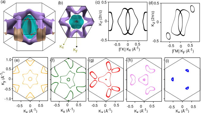
We now focus on the FS, in the vicinity of the DP. The side and top view of the 3D FS distribution within the Wigner-Seitz cell at for the relaxed structure is presented in Fig. 3(a) and (b), respectively. The presence of three contributing bands, each having twofold Kramer’s degeneracy, can be clearly seen. The outer-most part of the FS arises from the electron pocket of the first unoccupied band of CoTe2, as seen in Fig. 1(c). The type-II nature of the DSM phase is also confirmed by the fact that the Dirac point appears at the four-fold degenerate touching point of the other electron and hole pockets in the middle, as marked by the red arrow in the FS in Fig. 3(a). The energy contours over the and the planes, for is shown in Fig. 3(c) and (d), respectively. Our calculations reveal a prominent Dirac crossing located at . The anisotropic nature of the FS along the direction persists even at the DP. The in-plane projection of the energy contours at the DP is presented in Fig. 3(e)-(i), for five different out-of-plane distances (or values). At , we observe a hexapetalus flower shape along with a small circle at its center. The electron pockets at transform into an isolated bean-shaped pattern with increasing magnitude as seen in Fig. 3(g)-(i). At approaching the vicinity of bulk DP, the central contour converges to a tiny circle while the hexagonal outer contour acquires an almost triangular shape [see Fig. 3(g) and (h)]. Finally, at = 0.3, the FS cut appears as two contours centered around the origin, which exhibit a circular and triangular shape for the inner and outer contours, respectively. In addition, there are small pockets along three of the six lines [see Fig. 3(h)]. The energy contour at negative values with the same magnitude shows the rest of the three small pockets along the other lines. In Fig. 3(i) the inner contours vanish and we only see three small pockets along to direction.
V Origin of Dirac states, band inversion, and the Surface States
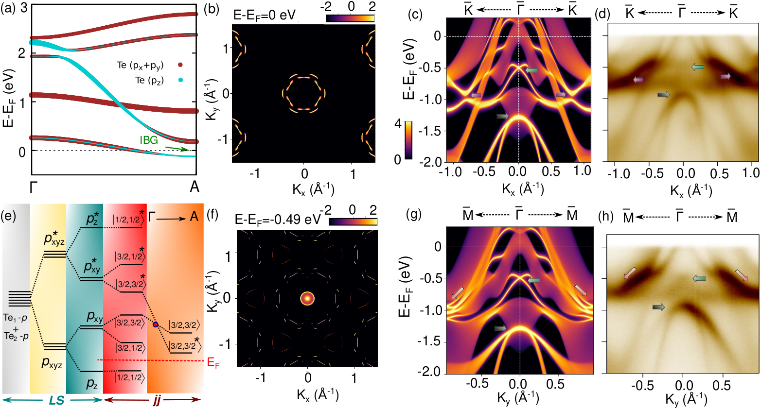
The presence of type-II Dirac fermions in the bulk dispersion of CoTe2 suggests the strong possibility of finding topologically protected surface states near the Fermi energy. Additionally, the bulk bands of CoTe2 also support several other topological band inversions in its bulk. In Fig. 4(a), the orbital-resolved band structure along the -A path shows that the linear crossings near are mainly composed of the Te-5 orbitals. The Dirac band crossing near 0.92 eV above Fermi energy arises from the interplay of the Te and the Te orbitals. Additionally, we find that these orbitals also contribute to multiple band inversion gaps along different high symmetry paths including [see Fig. 4(a)]. To understand the origin of the Dirac band crossing, we show the systematic evolution of the energy levels of the Te- orbital manifold in Fig. 4(e). The six degenerate orbital splits into lower (upper) lying three-fold bonding (anti-bonding) orbitals due to inter-site hybridization. The presence of local trigonal distortion of the Co-Te octahedra further lifts the degeneracy of the bonding/anti-bonding orbitals breaking it into singly degenerate () and doubly degenerate () orbitals. Including the SOC splits the orbitals into fourfold and two-fold pseudo spin basis as shown in the fourth column of Fig. 4(e). The last column of Fig. 4(e) highlights the effect of the dispersion along the direction. The bulk type-II Dirac point arises from the crossing of the bonding and anti-bonding states of the orbitals.
The ladder of multiple band inversions and the Dirac point in the bulk band structure points to the existence of topologically protected surface states in CoTe2. This is confirmed by our experiments and theoretical calculations. The measured ARPES results and the corresponding theoretical spectral function of the relaxed structure are shown along the high symmetry -- and -- directions in Fig. 4(c), (d) and Fig. 4(g), (h), respectively. The pattern of the spectral function and position of the surface Dirac cone matches well between the theoretical calculations and experimental plots. However, the other sharp spectral functions [purple, and yellow arrows in Fig. 4(c), (d) and Fig. 4(g)] arising from the bulk and surface states are slightly off in energy (see Appendix A for detailed discussions). This can be due to several reasons including i) small variations in the structural parameters, ii) some ambiguity in the pseudopotential for capturing core states, iii) some impurities or stacking faults in the crystal which are not included in theoretical calculations, amongst others. We also note that as the Bulk Dirac cone is significantly above the Fermi energy, it cannot be directly observed or mapped via our occupied state ARPES data.
The ARPES measurements were done with = 75 eV, which corresponds to . Therefore these spectra capture the bulk bands along with the surface states. The prominent features corresponding to the surface states, in the measured ARPES spectrum and the calculated spectral function are marked by thick arrows. Despite some discrepancies in the binding energy of a few states, the experimental and the theoretical results show good qualitative agreement. The small energy difference in the location of the surface states possibly arises due to structural effects or from the surface potential which is not included in our theoretical calculations.
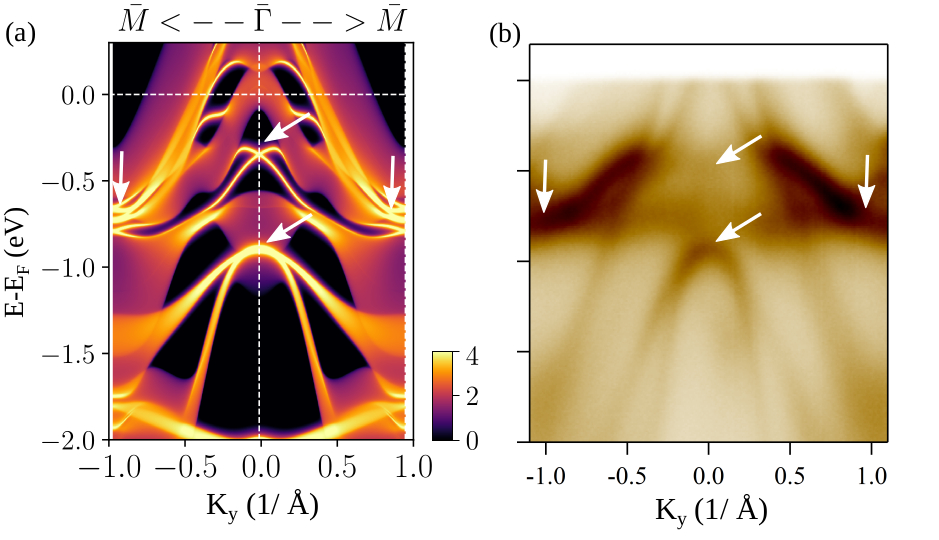
The Dirac cone in the surface states is located at the point at an energy 0.49 eV below the Fermi energy. The presence of a topological band inversion near , as marked by an arrow in Fig. 4 (a) gives rise to this surface Dirac crossing observed in ARPES. A similar surface Dirac cone, which has relatively broad features in ARPES experiments compared to theoretical calculations, has also been observed in other isostructural compounds such as NiTe2 and in PtTe2. Other than the Dirac cone at the point, several sharp non-trivial surface states appear near the high symmetry point and along the path. These arise from the multiple band inversions throughout the BZ. We find the surface states to be symmetric along both the -- and the -- directions.
The Fermi arc states at constant energy are plotted in Fig. 4 (b) at eV and in Fig. 4 (f) at eV. At the Fermi energy, circular arcs of the sharp surface states appear around the point. In contrast, a prominent peak is observed exactly at the point Fig. 4 (f) which captures the dominant surface Dirac, crossing along with a few less intense circular arcs along the - paths. There is another set of high-intensity surface arc states around eV below [see Fig. 4 (c) and (g)], which disperse symmetrically around the point.
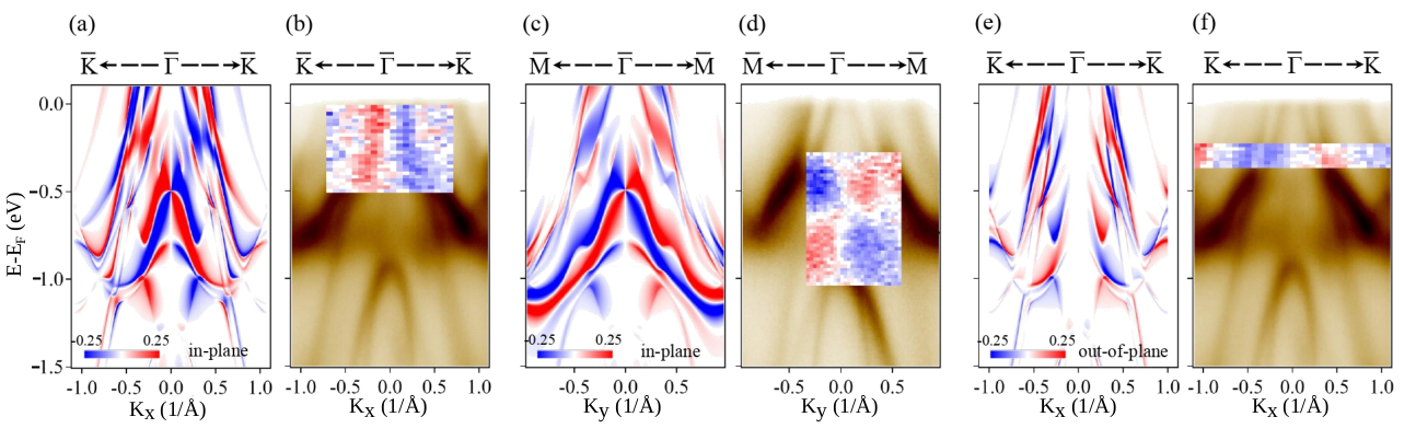
VI Spin polarized surface states
The demonstration of topological surface states in CoTe2 inspires the exploration of their spin-polarization. To study the spin polarization of the surface states and the surface Dirac cone, we experimentally measured the spin-polarized ARPES spectrum of CoTe2, as shown in Fig. 5(b), (d) and (f). The component of probed spin components is chosen to be perpendicular to the direction of the dispersion. The corresponding theoretically calculated spin resolved spectral function is shown in Fig. 5(a), (c), and (e). Figures 5(b) and (d) display the measured spin-resolved band structures superimposed onto the measured spin-integrated band structures shown in Figs. 4(d) and (h), along -- and --, respectively. As was seen in the experimental plots of Fig. 4(d) and (h), the surface Dirac cone spectral intensity is relatively low compared to the observed bulk states for the photon energy = 75 eV. Accordingly, its contribution to the measured spin-ARPES spectra is also small. To improve the resolution of the spin information of the surface Dirac cone, the Spin-ARPES spectra in Fig. 5(d) were measured with = 19 eV. The crossing of the up-spin (red) and the down-spin (blue) bands are well observed around the energy of the surface Dirac point, matching well with the calculated spin texture shown in Fig. 5(c). This confirms the helical nature of the spin-momentum locking around the surface Dirac point and its topological origin. The signs of measured and the calculated spin polarization is reversed for , in all panels. This implies that the spin polarization is not due to the breaking of time-reversal symmetry.
Interestingly, we also observe a significant contribution of the out-of-plane component in our spin ARPES experiments and calculations for the -- direction, as shown in Fig. 5(e) and (f). The measurement is done with incident photons with energy eV. The corresponding out-of-plane spin component for the -- direction is negligibly small. The scale of the in-plane and the out-of-plane spin polarization in all the panels is identical. Note that due to the presence of time reversal and inversion symmetry in CoTe2, the spin polarization of the bulk states is forbidden. Even an isolated monolayer of CoTe2 preserves the inversion and the time-reversal symmetries. Thus, an isolated monolayer of CoTe2 will also not support spin-polarized states. However, in a system of finite size, the inversion symmetry is broken for the atomic layers near the surface even for bulk centrosymmetric systems. This is what allows for spin polarization of the surface states (both in-plane and out-of-plane) in a finite slab of CoTe2, and other Dirac semimetals. Another interesting point is that the surface states near the point primarily arise from the topological bulk band inversions, and these lead to Dirac surface states which have an in-plane Rashba-like spin momentum locking. This can be clearly seen in Fig. 5(e), where the out-of-plane spin states are completely absent near the point.
VII Conclusions
In summary, based on the ARPES experiments combined with detailed first principle calculations, we show that CoTe2 hosts a pair of type-II Dirac nodes. The Dirac node is located along the axis around 0.92 eV above the Fermi energy, and they support Lorentz symmetry violating Dirac fermions. We find that in addition to the Dirac fermions, bulk CoTe2 also hosts several topological band inversions which give rise to a ladder of spin-polarized surface states over a wide range of energies. The surface states corresponding to the bulk band inversions form a surface Dirac cone at the point, which has Rashba-type in-plane spin splitting. Interestingly, we find that some surface states in CoTe2 also support an out-of-plane spin polarization. Our study highlights that CoTe2 supports interesting bulk and surface Dirac fermiology, which should be explored further in transport, optical, plasmonic, and optoelectronic experiments.
VIII Acknowledgement
A.C. acknowledges the Indian Institute of Technology, Kanpur, and the Science and Engineering Research Board (SERB) National Postdoctoral Fellowship (PDF/2021/000346), India for financial support. We thank Debasis Dutta and Barun Ghosh for the useful discussions. We acknowledge the Science and Engineering Research Board (SERB) and the Department of Science and Technology (DST) of the Government of India for financial support. We thank CC-IITK for providing the High-Performance Computing facility. This work has been partly performed in the framework of the nanoscience foundry and fine analysis (NFFA-MIUR Italy, Progetti Internazionali) facility.
Appendix A Scaled ARPES
The prominent bulk and surface states (except the Dirac crossing) of theoretically calculated spectral function and experimentally measured ARPES plots in Fig. 4(c), (d) and in Fig. 4(g)] have an energy difference of 500 meV. This can arise from various factors as discussed in section V. For example, a similar discrepancy of energy is reported for a related compound PtSe2 in Ref. Bahramy et al. (2018). An energy scale factor of 1.05 and an energy offset of -0.1 eV is necessary for the PtSe2 compound to correctly match the energy between theoretical and experimental ARPES results. Similarly in our calculation, an energy scaling of 0.7 can be used to best fit the experimental plot (see Fig. 6).
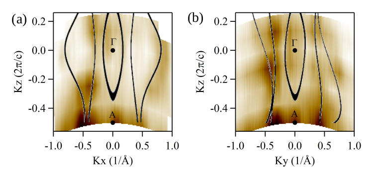
Appendix B Fermi surface anisotropy
In this section, we have compared the theoretically calculated and experimentally observed Fermi surface maps on - and - planes. In Fig. 7, we have plotted the theoretically calculated 2D energy contours at on top of the experimental results. Here the anisotropy, as discussed in section IV is evident from the differences between Fig. 7 (a) and Fig. 7 (b) plots. The experimental and maps are taken with the photon energy range between 55 eV and 85 eV.
References
- Yin et al. (2021) X. Yin, C. S. Tang, Y. Zheng, J. Gao, J. Wu, H. Zhang, M. Chhowalla, W. Chen, and A. T. S. Wee, Chemical Society Reviews 50, 10087 (2021).
- Zhang et al. (2020) X. Zhang, S. Y. Teng, A. C. M. Loy, B. S. How, W. D. Leong, and X. Tao, Nano Materials 10, 1012 (2020).
- Fiori et al. (2014) G. Fiori, F. Bonaccorso, G. Iannaccone, T. Palacios, D. Neumaier, A. Seabaugh, S. K. Banerjee, and L. Colombo, Nature Nanotechnology 9, 768 (2014).
- Wang et al. (2016) Q. Wang, J. Lai, and D. Sun, Optical Materials Express 6, 2313 (2016).
- Chang et al. (2021) L. Chang, Z. Sun, and Y. H. Hu, Electrochamical Energy Reviews 4, 194 (2021).
- Vobornik et al. (2021) I. Vobornik, A. B. Sarkar, L. Zhang, D. W. Boukhvalov, B. Ghosh, L. Piliai, C.-N. Kuo, D. Mondal, J. Fujii, C. S. Lue, M. Vorokhta, H. Xing, L. Wang, A. Agarwal, and A. Politano, Advanced Functional Materials 31, 2106101 (2021).
- D’Olimpio et al. (2022) G. D’Olimpio, L. Zhang, C.-N. Kuo, D. Farias, L. Ottaviano, C. S. Lue, J. Fujii, I. Vobornik, A. Agarwal, P. Torelli, D. W. Boukhvalov, and A. Politano, Nanomaterials 12 (2022), 10.3390/nano12030558.
- Tang et al. (2017) S. Tang, C. Zhang, D. Wong, Z. Pedramrazi, H.-Z. Tsai, C. Jia, B. Moritz, M. Claassen, H. Ryu, S. Kahn, J. Jiang, H. Yan, M. Hashimoto, D. Lu, R. G. Moore, C.-C. Hwang, C. Hwang, Z. Hussain, Y. Chen, M. M. Ugeda, Z. Liu, X. Xie, T. P. Devereaux, M. F. Crommie, S.-K. Mo, and Z.-X. Shen, Nature Physics 13, 683 (2017).
- Chen et al. (2018) P. Chen, W. W. Pai, Y.-H. Chan, W.-L. Sun, C.-Z. Xu, D.-S. Lin, M. Y. Chou, A.-V. Fedorov, and T.-C. Chiang, Nature Communications 9, 2003 (2018).
- Liu et al. (2012) D. Liu, W. Zhang, D. Mou, J. He, Y.-B. Ou, Q.-Y. Wang, Z. Li, L. Wang, L. Zhao, S. He, Y. Peng, X. Liu, C. Chen, L. Yu, G. Liu, X. Dong, J. Zhang, C. Chen, Z. Xu, J. Hu, X. Chen, X. Ma, Q. Xue, and X. J. Zhou, Nature Communications 3, 931 (2012).
- Miyata et al. (2015) Y. Miyata, K. Nakayama, K. Sugawara, T. Sato, and T. Takahashi, Nature Materials 14, 775 (2015).
- Chen et al. (2015) P. Chen, Y.-H. Chan, X.-Y. Fang, Y. Zhang, M. Y. Chou, S.-K. Mo, Z. Hussain, A.-V. Fedorov, and T.-C. Chiang, Nature Communications 6, 8943 (2015).
- Clark et al. (2018a) O. J. Clark, M. J. Neat, K. Okawa, L. Bawden, I. Marković, F. Mazzola, J. Feng, V. Sunko, J. M. Riley, W. Meevasana, J. Fujii, I. Vobornik, T. K. Kim, M. Hoesch, T. Sasagawa, P. Wahl, M. S. Bahramy, and P. D. C. King, Phys. Rev. Lett. 120, 156401 (2018a).
- Noh et al. (2017) H.-J. Noh, J. Jeong, E.-J. Cho, K. Kim, B. I. Min, and B.-G. Park, Phys. Rev. Lett. 119, 016401 (2017).
- Alicea et al. (2011) J. Alicea, Y. Oreg, G. Refael, F. von Oppen, and M. P. A. Fisher, Nature Physics 7, 412 (2011).
- Chiu et al. (2021) W.-C. Chiu, S. Mardanya, R. Markiewicz, J. Nieminen, B. Singh, T. Hakioglu, A. Agarwal, T.-R. Chang, H. Lin, and A. Bansil, “Topological charge density wave in monolayer nbse2,” (2021).
- Emmanouilidou et al. (2020) E. Emmanouilidou, S. Mardanya, J. Xing, P. V. S. Reddy, A. Agarwal, T.-R. Chang, and N. Ni, Phys. Rev. B 102, 235144 (2020).
- Ghosh et al. (2019) B. Ghosh, D. Mondal, C.-N. Kuo, C. S. Lue, J. Nayak, J. Fujii, I. Vobornik, A. Politano, and A. Agarwal, Physical Review B 100, 195134 (2019).
- Anemone et al. (2021) G. Anemone, P. Casado Aguilar, M. Garnica, F. Calleja, A. Al Taleb, C.-N. Kuo, C. S. Lue, A. Politano, A. L. Vázquez de Parga, G. Benedek, D. Farías, and R. Miranda, npj 2D Materials and Applications 5, 25 (2021).
- Yan et al. (2017) M. Yan, H. Huang, K. Zhang, E. Wang, W. Yao, K. Deng, G. Wan, H. Zhang, M. Arita, H. Yang, Z. Sun, H. Yao, Y. Wu, S. Fan, W. Duan, and S. Zhou, Nature Communications 8, 257 (2017).
- Zhang et al. (2017) K. Zhang, M. Yan, H. Zhang, H. Huang, M. Arita, Z. Sun, W. Duan, Y. Wu, and S. Zhou, Phys. Rev. B 96, 125102 (2017).
- Kang et al. (2017) M. Kang, B. Kim, S. H. Ryu, S. W. Jung, J. Kim, L. Moreschini, C. Jozwiak, E. Rotenberg, A. Bostwick, and K. S. Kim, Nano Letters 17, 1610 (2017).
- He and Que (2016) Z. He and W. Que, Applied Materials Today 3, 23 (2016).
- Manzeli et al. (2017) S. Manzeli, D. Ovchinnikov, D. Pasquier, O. V. Yazyev, and A. Kis, Nature Reviews Materials 2 (2017), 10.1038/natrevmats.2017.33.
- Zheng et al. (2016) F. Zheng, C. Cai, S. Ge, X. Zhang, X. Liu, H. Lu, Y. Zhang, J. Qiu, T. Taniguchi, K. Watanabe, S. Jia, J. Qi, J.-H. Chen, D. Sun, and J. Feng, Advanced Materials 28, 4845 (2016).
- Mak et al. (2010) K. F. Mak, C. Lee, J. Hone, J. Shan, and T. F. Heinz, Physical Review Letters 105 (2010), 10.1103/PhysRevLett.105.136805.
- Hlevyack et al. (2021) J. A. Hlevyack, L.-Y. Feng, M.-K. Lin, R. A. B. Villaos, R.-Y. Liu, P. Chen, Y. Li, S.-K. Mo, F.-C. Chuang, and T.-C. Chiang, npj 2D Materials and Applications 5, 40 (2021).
- Mukherjee et al. (2020) S. Mukherjee, S. W. Jung, S. F. Weber, C. Xu, D. Qian, X. Xu, P. K. Biswas, T. K. Kim, L. C. Chapon, M. D. Watson, J. B. Neaton, and C. Cacho, Scientific Reports 10, 12957 (2020).
- Anemone et al. (2020) G. Anemone, M. Garnica, M. Zappia, P. C. Aguilar, A. A. Taleb, C.-N. Kuo, C. S. Lue, A. Politano, G. Benedek, A. L. V. de Parga, R. Miranda, and D. Farías, 2D Materials 7, 025007 (2020).
- Huang et al. (2016) H. Huang, S. Zhou, and W. Duan, Phys. Rev. B 94, 121117 (2016).
- Fei et al. (2017) F. Fei, X. Bo, R. Wang, B. Wu, J. Jiang, D. Fu, M. Gao, H. Zheng, Y. Chen, X. Wang, H. Bu, F. Song, X. Wan, B. Wang, and G. Wang, Phys. Rev. B 96, 041201 (2017).
- Clark et al. (2018b) O. J. Clark, M. J. Neat, K. Okawa, L. Bawden, I. Marković, F. Mazzola, J. Feng, V. Sunko, J. M. Riley, W. Meevasana, J. Fujii, I. Vobornik, T. K. Kim, M. Hoesch, T. Sasagawa, P. Wahl, M. S. Bahramy, and P. D. C. King, Phys. Rev. Lett. 120, 156401 (2018b).
- Politano et al. (2018a) A. Politano, G. Chiarello, C.-N. Kuo, C. S. Lue, R. Edla, P. Torelli, V. Pellegrini, and D. W. Boukhvalov, Advanced Functional Materials 28, 1706504 (2018a).
- Nurmamat et al. (2021) M. Nurmamat, S. V. Eremeev, X. Wang, T. Yoshikawa, T. Kono, M. Kakoki, T. Muro, Q. Jiang, Z. Sun, M. Ye, and A. Kimura, Phys. Rev. B 104, 155133 (2021).
- Rizza et al. (2022) C. Rizza, D. Dutta, B. Ghosh, F. Alessandro, C.-N. Kuo, C. S. Lue, L. S. Caputi, A. Bansil, V. Galdi, A. Agarwal, A. Politano, and A. Cupolillo, ACS Applied Nano Materials (2022), 10.1021/acsanm.2c04340.
- Politano et al. (2018b) A. Politano, G. Chiarello, B. Ghosh, K. Sadhukhan, C.-N. Kuo, C. S. Lue, V. Pellegrini, and A. Agarwal, Phys. Rev. Lett. 121, 086804 (2018b).
- Xu et al. (2018) C. Xu, B. Li, W. Jiao, W. Zhou, B. Qian, R. Sankar, N. D. Zhigadlo, Y. Qi, D. Qian, F.-C. Chou, and X. Xu, Chemistry of Materials 30, 4823 (2018).
- Zhang et al. (2021) L. Zhang, Z. Chen, K. Zhang, L. Wang, H. Xu, L. Han, W. Guo, Y. Yang, C.-N. Kuo, C. S. Lue, D. Mondal, J. Fuji, I. Vobornik, B. Ghosh, A. Agarwal, H. Xing, X. Chen, A. Politano, and W. Lu, Nature Communications 12, 1584 (2021).
- Aguilar et al. (2022) P. C. Aguilar, F. Calleja, C.-N. Kuo, C. S. Lue, B. Ghosh, A. Agarwal, A. Politano, A. L. V. de Parga, R. Miranda, J. A. Silva-Guillén, and M. Garnica, Journal of Physics: Materials 5, 044003 (2022).
- Note (1) Zhen Hu1, Libo Zhang, Atasi Chakraborty, Gianluca D’Olimpio, Jun Fujii, Amit Agarwal, Ivana Vobornik, Daniel Farias, Changlong Liu, Chia-Nung Kuo, Chin Shan Lue, Li Han, Kaixuan Zhang, Zhiqingzi Chen, Chenyu Yao, Anping Ge, Yuanchen Zhou, Antonio Politano, Weida Hu, Shao-Wei Wang, Lin Wang, Xiaoshuang Chen and Wei Lu, Terahertz Nonlinear Hall Rectifier Based on Spin-Polarized 1T-CoTe2, To appear in Adv. Mater.
- Lu et al. (2015) T.-H. Lu, C.-J. Chen, M. Basu, C.-G. Ma, and R.-S. Liu, Chemical Communications 51, 17012 (2015).
- Chia et al. (2017) X. Chia, Z. Sofer, J. Luxa, and M. Pumera, Chemistry-A European Journal 23, 11719 (2017).
- Perdew et al. (1996) J. P. Perdew, K. Burke, and M. Ernzerhof, Physical Review Letters 77, 3865 (1996).
- Blöchl (1994) P. E. Blöchl, Physical Review B 50, 17953 (1994).
- Kresse and Joubert (1999a) G. Kresse and D. Joubert, Physical Review B 59, 1758 (1999a).
- Kresse and Furthmüller (1996) G. Kresse and J. Furthmüller, Physical Review B 54, 11169 (1996).
- Kresse and Joubert (1999b) G. Kresse and D. Joubert, Physical Review B 59, 1758 (1999b).
- Monkhorst and Pack (1976) H. J. Monkhorst and J. D. Pack, Physical Review B 13, 5188 (1976).
- Marzari and Vanderbilt (1997) N. Marzari and D. Vanderbilt, Physical Review B 56, 12847 (1997).
- Wu et al. (2018) Q. Wu, S. Zhang, H.-F. Song, M. Troyer, and A. A. Soluyanov, Computer Physics Communication 224, 405 (2018).
- Panaccione et al. (2009) G. Panaccione, I. Vobornik, J. Fujii, D. Krizmancic, E. Annese, L. Giovanelli, F. Maccherozzi, F. Salvador, A. De Luisa, D. Benedetti, A. Gruden, P. Bertoch, F. Polack, D. Cocco, G. Sostero, B. Diviacco, U. Hochstrasser, M. Maier, D. Pescia, C. Back, T. Greber, J. Osterwalder, M. Galaktionov, M. Sancrotti, and G. Rossi, Review of Scientific Instruments 80, 043105 (2009).
- Bigi et al. (2017) C. Bigi, K. Pranab, D. Benedetti, F. Salvador, D. Krizmancic, R. Sergo, A. Martin, G. Panaccione, G. Rossi, J. Fujii, and I. Vobornik, J. Synchrotron Rad. 24, 750 (2017).
- Nappini et al. (2020) S. Nappini, D. W. Boukhvalov, G. D’Olimpio, L. Zhang, B. Ghosh, C.-N. Kuo, H. Zhu, J. Cheng, M. Nardone, L. Ottaviano, D. Mondal, R. Edla, J. Fuji, C. S. Lue, I. Vobornik, J. A. Yarmoff, A. Agarwal, L. Wang, L. Zhang, F. Bondino, and A. Politano, Advanced Functional Materials 30, 2000915 (2020).
- Damascelli (2004) A. Damascelli, Physica Scripta T109, 61 (2004).
- Bahramy et al. (2018) M. Â. S. Bahramy, O. Â. J. Clark, B.-J. Yang, J. Feng, L. Bawden, J. Â. M. Riley, I. Marković, F. Mazzola, V. Sunko, D. Biswas, S. Â. P. Cooil, M. Jorge, J. Â. W. Wells, M. Leandersson, T. Balasubramanian, J. Fujii, I. Vobornik, J. E. Rault, T. Â. K. Kim, M. Hoesch, K. Okawa, M. Asakawa, T. Sasagawa, T. Eknapakul, W. Meevasana, and P. Â. D. Â. C. King, Nature Materials 17, 21 (2018).