Gate-controlled Magnetotransport and Electrostatic Modulation of
Magnetism in 2D magnetic semiconductor CrPS4
Abstract
Using field-effect transistors (FETs) to explore atomically thin magnetic semiconductors with transport measurements is difficult, because the very narrow bands of most 2D magnetic semiconductors cause carrier localization, preventing transistor operation. Here, we show that exfoliated layers of CrPS4 –a 2D layered antiferromagnetic semiconductor whose bandwidth approaches 1 eV– allow the realization of FETs that operate properly down to cryogenic temperature. Using these devices, we perform conductance measurements as a function of temperature and magnetic field, to determine the full magnetic phase diagram, which includes a spin-flop and a spin-flip phase. We find that the magnetoconductance depends strongly on gate voltage, reaching values as high as 5000 % near the threshold for electron conduction. The gate voltage also allows the magnetic states to be tuned, despite the relatively large thickness of the CrPS4 multilayers employed in our study. Our results show the need to employ 2D magnetic semiconductors with sufficiently large bandwidth to realize properly functioning transistors, and identify a candidate material to realize a fully gate-tunable half-metallic conductor.
Atomically thin van der Waals (vdW) semiconducting magnets (i.e., 2D magnets) exhibit phenomena resulting from the interplay between semiconducting and magnetic functionalities, absent in other material platforms 1, 2, 3. Recently reported examples include the observation of a strong electric field modulation of the spin-flip field in CrI3 bilayers 4, 5, of the dependence of the luminescence wavelength on the magnetic state of CrSBr 6, and of giant tunneling magnetoresistance of barriers made of 2D magnetic multilayers 7, 8, 9, 10, 11, 12. Theory predicts more phenomena that remain to be observed, such as the possibility to create gate-tunable half-metallic conductors by populating fully spin-polarized bands of 2D semiconductors 13, 14, 15. Experiments, however, have been drastically limited by the extremely narrow bandwidths of most 2D magnetic semiconductors explored so far (frequently meV) 16, 17, which causes these materials to behave very differently from conventional high-quality semiconductors such as Si or GaAs. Indeed, in narrow bandwidth semiconductors Coulomb interactions and disorder potentials easily exceed the kinetic energy of charge carriers, often resulting in their localization. To progress, it is essential to identify 2D semiconducting compounds with the largest possible bandwidth.
These considerations are particularly pertinent for the realization of field-effect transistors (FETs) enabling gate-tunable transport measurements well below the magnetic transition temperature . For the majority of 2D magnets investigated so far (e.g., Chromium Trihalides 7, 8, 9, 10, 11, 12, MnPS3 18), either no transistor action was observed, or the devices were found to exhibit extremely poor characteristics and to function exclusively for >. In materials such as VI3 or Cr2Ge2Te6 the bandwidth is slightly larger (a few hundreds meV 19 and 0.5 eV 20, 21, respectively) and clear transistor action is seen, but even then experiments are drastically limited by the device quality 22, 23, 24, 25. Very recently, CrSBr –whose bandwidth exceeds 1.5 eV 6, 26– and NiI2 –whose bandwidth is estimated to be 0.8-1 eV 27– enabled the first realization of FETs operating down to cryogenic temperature 26, 28, confirming that a large bandwidth is indeed key to observe gate-induced in-plane transport at low-temperatures in these systems. However, in neither of these two compounds electrostatic modification of their magnetic phase boundaries has been reported.Currently, therefore, identifying more 2D magnetic semiconductors with a sufficiently large bandwidth to realize FETs enabling the magnetic state of 2D magnetic semiconductors to be probed –and possibly controlled– remains a key target.
Here, we explore CrPS4 –a 2D semiconducting layered antiferromagnet, whose bandwidth approaches 1 eV– to show experimentally that FETs based on this material operate properly up to the lowest temperature reached in our experiments ( = 250 mK), and to demonstrate that the magnetic state of the material can be tuned by acting on the gate voltage . Measurements at fixed show that the dependence of the device conductance on temperature and applied magnetic field enables the boundaries between the different magnetic states of CrPS4 to be precisely determined. With magnetic field applied perpendicular to the layers, the magnetoconductance exhibits clear features associated to the spin-flop and spin-flip transitions –at respectively T and T, at T = 2 K– that shift to smaller fields upon increasing , before eventually disappearing for (the Néel temperature of CrPS4 multilayers, K). When the field is applied parallel to the layers, the behavior and magnitude of the magnetoconductance are similar, except for the absence of the spin-flop transition (as expected, since in CrPS4 the easy axis is perpendicular to the layers). The dependence of transport on shows the possibility to drastically increase the magnetoconductance, which exceeds 5000 % as approaches the threshold voltage. A shift of the spin-flip and spin-flop fields, as well as of , is also unambiguously detected, signaling that the magnetic state can be gate-tuned. Besides confirming that large bandwidth 2D magnetic semiconductors enable the magnetic state of 2D magnetic semiconductors to be probed by means of magnetotransport and to be tuned electrostatically, our results identify a first viable experimental candidate for the realization of a gate tunable half-metallic conductor.
I Results and Discussion
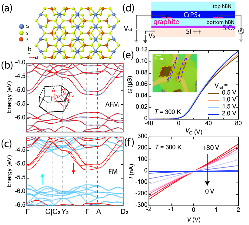
CrPS4 crystallizes into a monoclinic structure formed by the vdW stacking of distorted CrS6 octahedra and PS4 tetrahedra as shown in Figure 1a 29, 30, 31, 32, 33, 15, 34. It is an air-stable, weakly anisotropic layered antiferromagnet with an easy axis perpendicular to the layers 32, 35, 36. The Néel temperature – = 38 K in bulk crystals– is somewhat reduced in atomically thin exfoliated multilayers 32, 35, 36. Band structure calculations for the antiferromagnetic and ferromagnetic spin configurations of the material (see Figure 1b and 1c) show that the conduction band is fully spin-polarized in the ferromagnetic state and in individual monolayers, potentially enabling the realization of a fully gate-tunable half-metallic conductors if gate-induced transport at low temperature can be achieved 15. Most importantly, the calculations also show that the conduction band disperses by approximately 1 eV, which is the main reason for us to select this system to nano-fabricate FET devices.
CrPS4 crystals purchased from HQ Graphene are characterized by energy dispersive X-Ray and Raman spectroscopy (see supplementary information), then exfoliated with an adhesive tape, and transferred onto doped silicon substrates covered with a 285 nm thick thermally grown oxide layer (see Figure 1d). Using by now conventional pick-up and transfer techniques 37, selected exfoliated layers are placed onto bottom multilayer graphene strips acting as source and drain electrodes, and encapsulated between 20-30 nm thick h-BN crystals. Even though the material is air-stable, exfoliation, transfer and encapsulation are performed in a glove-box with sub-ppm concentration of oxygen and water to maximize the quality of the final device. The structures are then taken out of the glove-box and metal contacts are attached to the graphene strips by means of electron beam lithography, reactive ion etching of the top hBN layer with a CF4/O2 mixture, electron beam evaporation of a Cr-Au film (20/30 nm), and lift-off. An optical microscope image of one of our devices is shown in the inset of Figure 1e. We realized devices containing multiple transistors on 4 different exfoliated CrPS4 multilayers, with thickness in the 6-11 nm range (as determined by atomic force microscopy), all exhibiting comparable behavior.
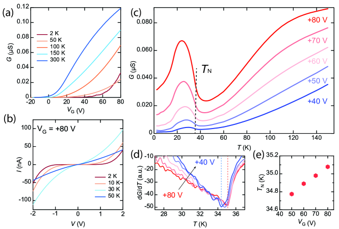
Multilayer CrPS4 FETs exhibit transfer curves (conductance versus ) typical of -type semiconductors, as shown in Figure 1e with data measured on a 10 nm thick device, whose behavior is representative of that of all transistors investigated in our work (all data shown in the main text have been measured on this same 10 nm device; data from another device are shown in the supplementary information to illustrate that our observations are reproducible). The relatively small threshold ( = +10 V) indicates that the Fermi level is located close to the conduction band edge, due to unintentional dopants present in the material. The field-effect (two-probe) mobility estimated from the room-temperature transconductance () of this device is 0.2 cm2 V-1 s-1. Other devices exhibit values reaching up to 1 cm2 V-1 s-1, comparable to values reported in CrSBr and NiI2 transistors, where measurements were performed in a four-probe configuration 26, 28. The output characteristics (source-drain current versus applied bias , measured for different ) are rather linear at room temperature (see Figure 1f), but upon cooling the behavior changes: the threshold voltages shift to larger positive values (as expected for a doped semiconductor; Figure 2a), and a pronounced non-linearity of the output characteristics becomes apparent (see Figure 2b; data measured at = +80 V), indicating the presence of a contact resistance. For applied biases > 1.0 V, however, the contacts appear not to influence significantly the measurements, as the extracted electron mobility becomes almost bias independent (see Fig. S3 in the supplementary information; at low temperature the mobility measured at > 1.0 V ranges between 1-4 cm2V-1s-1 depending on the device, again comparable to values extracted from four-terminal measurements in CrSBr and NiI2 26, 28). We conclude that the quality of our CrPS4 transistors is comparable to that of similar devices recently reported on CrSBr and NiI2, and that it is amply sufficient to allow transport to be measured to temperatures much lower than , and to be gate-tuned continuously. This conclusion confirms the need to select 2D magnetic semiconductors with sufficiently large bandwidth for the realization of transistors properly functioning at low temperature.
The onset of the magnetically ordered state in CrPS4 is clearly visible in the transistor conductance measured as a function of , at fixed . Upon cooling down the devices from room temperature, the conductance decreases slowly (as carriers freeze out into the dopants where they originate from 38), before exhibiting an abrupt increase as is lowered just below the Néel transition (see Figure 2c). The abrupt increase results from the transition into the layered antiferromagnetic state that occurs at 35 K (as determined by the position of the minimum of in Figure 2c), slightly lower than the value of TN in bulk CrPS4 crystals, confirming the trend demonstrated in recent magneto-optical studies that the critical temperature of CrPS4 decreases with decreasing thickness of the crystal 36. The observed conductance increase below TN is due to the onset of long-range spin ordering that suppresses disorder associated to spin fluctuations within each CrPS4 layer. At = +80 V the effect is sizable, as the conductance increases by more than a factor of 3 before eventually decreasing again and saturating at low temperature.
Whether the sizable increase in conductance upon passing from the paramagnetic to the antiferromagnetic state implies that the devices should also exhibit sizable magnetoconductance (since an applied magnetic field can modify the magnetic state of the material) is not clear a priori. Large magnetoconductance in magnetic materials commonly occurs when the current flows across regions with spatially inhomogeneous magnetization (such as domain walls 39, 40, 41, spin valves 42, 43, tunnel barriers made of layered antiferromagnetic insulators 7, 8, 9, 10, 11, 12, etc.). This is not the case in our FETs, since the current in the transistor channel propagates parallel to the CrPS4 layers, and the magnetization of each layer is uniform at low temperatures. Another known mechanism that –by analogy– may seem relevant for our devices is the one responsible for the magnetoconductance of metallic magnetic multilayers 44, 45, 46. When current flows parallel to the layers, the conductance is typically higher in the ferromagnetic state (i.e., when all layers are magnetized in the same direction) than in the antiferromagnetic one (when adjacent layers are magnetized in opposite directions), because the different scattering rates of majority and minority spin electrons result in a different electron mobility in the two magnetic states 47. This mechanism normally leads to magnetoconductance values well below 100 % (i.e., changes that are less than a factor of two), i.e., smaller than the change that associated to the transition from the paramagnetic to the antiferromagnetic state upon lowering (with = +80 V see Figure 2c). There is therefore no established mechanism suggesting that a very large magnetoconductance should be observed in CrPS4 FETs for < , and indeed, recent measurements on FETs based on CrSBr and NiI2 26, 28 –which are also 2D semiconducting layered antiferromagnets– have shown only a modest magnetoconductance (well below a factor of two).
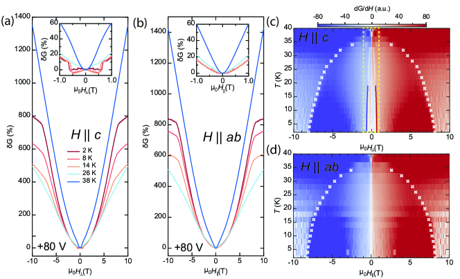
Figures 3 and 4 show that –in contrast to CrSBr and NiI2 transistors– CrPS4 FETs do exhibit a very large magnetoconductance, which appears upon cooling, as the Néel temperature is approached. The large magnetoconductance (see Figures 3a and 3b) observed above and just below the critical temperature originates from spin fluctuations, because in this temperature range (i.e., in the paramagnetic state or in the antiferromagnetic one, when magnetic order is not yet fully developed) the magnetic susceptibility is largest, so that the applied magnetic field is most effective in polarizing the spins and thereby in reducing spin-induced disorder 48. What is however more surprising and unexpected –because far below the magnetic state is robust and spins not easily polarizable– is that upon lowering the temperature further, the magnetoconductance remains large. Irrespective of whether the magnetic field is applied perpendicular or parallel to the layers, the magnetoconductance reaches values as large as a factor of 50 (i.e., 5000 %, seen Figure 3a and 3b), for an applied magnetic field = 10 T, and is gate tunable (the extremely strong, nearly exponential, dependence of on is shown in Figure 4b). Finding that the large magnetoconductance persists when the field is applied in the plane of CrPS4 –in conjunction with the low electron mobility– implies that the orbital effects of the magnetic field (as well as the influence of the graphene contacts) are not the reason for the observed large magnetotransport response. Indeed, the experiments indicate that the large magnetoconductance originates from the magnetic-field induced modifications of the magnetic state of CrPS4.
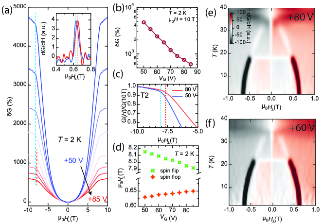
To illustrate the relationship between magnetoconductance and magnetic state we start by discussing Figure 3c and 3d, where we plot the derivative of the conductance as a function of field and temperature. For perpendicular fields (Figure 3a and Figure 3c), two distinct features are observed. First, for well below TN the conductance exhibits a kink and stops increasing rapidly above approximately 8 T (see Figure 3a). The phenomenon originates from the spin-flip transition, above which all spins fully align along the applied field (in the color plot of in Figure 3c, the transition –marked by the white diamonds– manifests itself in a more pronounced way, and can be followed all the way up TN). The second feature is a smaller, but clearly distinct change in magnetoconductance at much lower field (0.6 T at = 2 K), shown in the inset of Figure 3a, and clearly apparent in the region delimited by the yellow dashed line in Figure 3c. It is a manifestation of the spin-flop transition that occurs because CrPS4 is a weakly anisotropic layered antiferromagnet. The color plot of in Figure 3c illustrate clearly how the spin-flip and spin-flop fields decrease as the temperature is increased, and eventually vanish at approximately 35 K, i.e. the Néel temperature of the material. Similar considerations can be made by looking at Figure 3b and Figure 3d, when the magnetic field is applied parallel to the layers, but in that case no spin-flop transition is observed (as expected, since the easy axis of CrPS4 is perpendicular to the layers). Measuring the magnetoconductance of our FETs, therefore, allows us to trace the complete magnetic phase diagram of CrPS4 multilayers, and even to identify features that are often complex to detect experimentally in atomically thin layers (such as the spin-flop transition, which has not been detected in any exfoliated 2D magnet by means of magneto-optics experiments, the technique possibly the most commonly employed to study magnetism in these systems).
Having established the ability to map the magnetic phase diagram through magnetoconductance measurements, we analyze whether the different magnetic states can be influenced electrostatically, by varying the voltage applied to the gate. A strong effect is only expected in devices realized with crystals that are one or few layers thick because electrostatic screening forces the charge accumulated in the transistor channel to reside exclusively in the first few layers next to the gate electrode (in the range of accumulated electron densities –a few 1012 cm-2– the screening length is approximately 1 nm, which is why most charges are accumulated in the first CrPS4 layer next to the gate). Nevertheless –despite our devices being 10-to-20 monolayer thick– magnetoconductance measurements unambiguously show that systematic gate-induced changes in the magnetic state are present. To demonstrate this conclusion, we focus on specific points of the boundaries between the different magnetic phases that can be precisely determined, and look at their evolution upon varying .
First clear evidence for the modification of the CrPS4 phase boundaries by the electrostatic gate is seen in the critical temperature at zero applied magnetic field, which experimentally can be precisely determined by looking at the position of the minimum in (Figure 2d). Upon varying from +50 V to +80 V, the minimum in –and hence – increases by approximately 0.5 K (Figure 2e; in the different devices that we measured the change ranges between 0.5 to 1 K, see for instance Fig. S5 in the supplementary information for data from another transistor. Varying the gate voltage also affects the spin-flip transition field, which decreases by about 0.3 T when the gate is changed in approximately the same range at = 2 K (see the blue and red dashed line in Figure 4a and c), and modulates the spin-flop transition as well (compare Figure 4e and 4f): the magnetoconductance along the phase boundary changes and the spin-flop field increases by approximately 20 mT as is increased from +50 V to +85 V (see the inset of Figure 4a). The evolution of both transitions as a function of gate voltage is summarized in Figure 4d. Since, at the simplest level, the spin-flip field is proportional to the interlayer exchange interaction , and the spin-flop field to (where is the magnetic anisotropy) 49, finding that these two quantities change in opposite directions (the first decreases whereas the second increase as is increased) implies that both and are affected by the gate voltage.
Finding that CrPS4 FETs allow controlling the magnetic state electrostatically and probing the resulting changes by transport measurements is worth emphasizing because the only 2D magnetic semiconductors on which continuous FET operation could be achieved at low temperature so far (CrSBr 26 and NiI2 28) did not exhibit any modulation of the magnetic phase boundaries upon varying the gate voltage. Indeed, among all 2D magnetic semiconductors studied, only in mono and bilayers of CrI3 a continuous gate-tuning of the magnetic state has been observed, by means of magneto-optical techniques 5, 4. In that case, all layers were affected by the gate-accumulated (reaching up to 1013 cm-2) –owing to the atomic thickness of the material– and for monolayer CrI3, a 10 K gate-induced change in critical temperature was reported 5. In our transistors the effect is somewhat smaller, probably because the charge is accumulated predominantly in the individual layer closest to the gate electrode, but the CrPS4 multilayers are 10-to-20 layers thick, and we expect that in devices based on CrPS4 mono or bilayers a stronger dependence of the magnetic state on gate voltage will be observed. Exploring how the magnetic state depends on thickness and how thin multilayers are influenced by charge accumulation is certainly worth addressing in future work, to reveal the microscopic mechanism through which charge accumulation modifies magnetism that is currently unknown.
II Conclusion
The ability to accumulate electrostatically charge carriers at the surface of 2D magnetic semiconductors to induce electronic transport and control the magnetic state discloses opportunities for future experiments targeting unexplored phenomena. Identifying the microscopic mechanism responsible for the interplay between transport electrons and the magnetic state reported here –causing the magnetoconductance to reach values up to 5000 %– provides a first clear objective. More in general, the occurrence of gate-induced low-temperature transport in CrPS4 enables a much broader variety of experiments to be done, for instance in multi-terminal devices (e.g., to search for the anomalous Hall effect and investigate its gate dependence), in devices based on few-layer crystals (where the influence of gating on the magnetic state is expected to be much stronger), and in monolayers (where it will be possible to realize gate-tunable half-metallic conductors). Of great interest is also the implementation of local gates, to control the magnetic state locally in different parts of the device (to explore, for instance, whether the presence of interfaces between different magnetic states within the transistor channel allows the magnetoconductance to be increased even further). It should be realized, however, that the scope of possibilities is much broader, because CrPS4 is only the first large-bandwidth magnetic 2D semiconductor that enables the realization of transistors properly functioning at low temperature. We envision that many more 2D magnetic semiconductors with bandwidth comparable to (or larger than) that of CrPS4 will be introduced in the future, hosting a rich variety of magnetic states, providing experimental access to an even much broader variety of interesting physical phenomena.
Experimental section
Sample fabrication. CrPS4 multilayers were obtained by exfoliating bulk crystals, purchased from HQ Graphene, in a Nitrogen gas-filled glove box, with sub-ppm oxygen and water concentration to exclude any degradation and maximize the quality of the final device. The multilayer thickness was determined by means of atomic force microscopy. The multilayers were contacted electrically with few-layer graphene stripes and encapsulated with exfoliated hBN layers, employing a conventional pick-up and release technique based on PC/PDMS polymer stacks placed on glass slides. A total of 4 devices have been fabricated and the graphene stripes contacted with metallic electrodes (Cr/Au: 10/40 nm), using a conventional process based on electron-beam lithography, reactive ion etching, electron-beam evaporation, and lift-off.
Transport measurements. All transport measurements were performed in a Heliox 3He insert system (Oxford Instruments) equipped with a 15 T superconducting magnet. A Keithley 2400 source/measure was used to apply the gate voltage to the transistors. The bias voltage was applied using a homemade low-noise source. The current and voltage signals were amplified with homemade low-noise electronics and the amplified signals were recorded with an Agilent 34410A digital multimeter unit.
DFT calculations. First-principles simulations were performed using the Quantum ESPRESSO distribution 50, 51. To account for van der Waals interactions between the layers, the spin-polarised extension52 of the revised vdw-DF-cx exchange-correlation functional 53, 54 was adopted, which gives lattice parameters in good agreement with experiments. The Brillouin zone was sampled with a -centered Monkhorst-Pack grid, considering a doubled unit cell in the vertical direction (containing 24 atoms) both in the ferro- and antiferro-magnetic configurations. Pseudopotentials were taken from the Standard Solid-State Pseudopotential (SSSP) accuracy library (v1.0) 55 with cutoffs of 40 Ry and 320 Ry for wave functions and density, respectively. Atomic positions and lattice parameters were relaxed, reducing forces and stresses below thresholds of 3 meV/Å and 0.5 kbar, respectively. The band structure was computed along a high-symmetry path obtained by selecting the most interesting directions provided by SeekPath 56.
Acknowledgements
The authors gratefully acknowledge Alexandre Ferreira for continuous and valuable technical support. AFM gratefully acknowledges the Swiss National Science Foundation and the EU Graphene Flagship project for support. MG acknowledges support from the Italian Ministry for University and Research through the Levi-Montalcini program. KW and TT acknowledge support from the Elemental Strategy Initiative conducted by the MEXT, Japan (Grant Number JPMXP0112101001) and JSPS KAKENHI (Grant Numbers 19H05790, 20H00354 and 21H05233).
References
- Burch et al. [2018] K. S. Burch, D. Mandrus, and J.-G. Park, Nature 563, 47 (2018).
- Gibertini et al. [2019] M. Gibertini, M. Koperski, A. F. Morpurgo, and K. S. Novoselov, Nature Nanotechnology 14, 408 (2019).
- Mak et al. [2019] K. F. Mak, J. Shan, and D. C. Ralph, Nature Reviews Physics 1, 646 (2019).
- Huang et al. [2018] B. Huang, G. Clark, D. R. Klein, D. MacNeill, E. Navarro-Moratalla, K. L. Seyler, N. Wilson, M. A. McGuire, D. H. Cobden, D. Xiao, W. Yao, P. Jarillo-Herrero, and X. Xu, Nature Nanotechnology 13, 544 (2018).
- Jiang et al. [2018] S. Jiang, L. Li, Z. Wang, K. F. Mak, and J. Shan, Nature Nanotechnology 13, 549 (2018).
- Wilson et al. [2021] N. P. Wilson, K. Lee, J. Cenker, K. Xie, A. H. Dismukes, E. J. Telford, J. Fonseca, S. Sivakumar, C. Dean, T. Cao, X. Roy, X. Xu, and X. Zhu, Nature Materials 20, 1657 (2021).
- Klein et al. [2018] D. R. Klein, D. MacNeill, J. L. Lado, D. Soriano, E. Navarro-Moratalla, K. Watanabe, T. Taniguchi, S. Manni, P. Canfield, J. Fernández-Rossier, and P. Jarillo-Herrero, Science 360, 1218 (2018).
- Song et al. [2018] T. Song, X. Cai, M. W.-Y. Tu, X. Zhang, B. Huang, N. P. Wilson, K. L. Seyler, L. Zhu, T. Taniguchi, K. Watanabe, M. A. McGuire, D. H. Cobden, D. Xiao, W. Yao, and X. Xu, Science 360, 1214 (2018).
- Wang et al. [2018a] Z. Wang, I. Gutiérrez-Lezama, N. Ubrig, M. Kroner, M. Gibertini, T. Taniguchi, K. Watanabe, A. Imamoglu, E. Giannini, and A. F. Morpurgo, Nature Communications 9, 2516 (2018a).
- Ghazaryan et al. [2018] D. Ghazaryan, M. T. Greenaway, Z. Wang, V. H. Guarochico-Moreira, I. J. Vera-Marun, J. Yin, Y. Liao, S. V. Morozov, O. Kristanovski, A. I. Lichtenstein, M. I. Katsnelson, F. Withers, A. Mishchenko, L. Eaves, A. K. Geim, K. S. Novoselov, and A. Misra, Nature Electronics 1, 344 (2018).
- Kim et al. [2018] H. H. Kim, B. Yang, T. Patel, F. Sfigakis, C. Li, S. Tian, H. Lei, and A. W. Tsen, Nano Letters 18, 4885 (2018).
- Wang et al. [2019] Z. Wang, M. Gibertini, D. Dumcenco, T. Taniguchi, K. Watanabe, E. Giannini, and A. F. Morpurgo, Nature Nanotechnology 14, 1116 (2019).
- Li et al. [2014] X. Li, X. Wu, and J. Yang, Journal of the American Chemical Society 136, 11065 (2014).
- Gong et al. [2018] S.-J. Gong, C. Gong, Y.-Y. Sun, W.-Y. Tong, C.-G. Duan, J.-H. Chu, and X. Zhang, Proceedings of the National Academy of Sciences 115, 8511 (2018).
- Deng et al. [2021] J. Deng, J. Guo, H. Hosono, T. Ying, and X. Chen, Physical Review Materials 5, 034005 (2021).
- Wang et al. [2011] H. Wang, V. Eyert, and U. Schwingenschlögl, Journal of Physics: Condensed Matter 23, 116003 (2011).
- Zheng et al. [2019] Y. Zheng, X.-x. Jiang, X.-x. Xue, J. Dai, and Y. Feng, Physical Review B 100, 174102 (2019).
- Long et al. [2020] G. Long, H. Henck, M. Gibertini, D. Dumcenco, Z. Wang, T. Taniguchi, K. Watanabe, E. Giannini, and A. F. Morpurgo, Nano Letters 20, 2452 (2020).
- Kong et al. [2019] T. Kong, K. Stolze, E. I. Timmons, J. Tao, D. Ni, S. Guo, Z. Yang, R. Prozorov, and R. J. Cava, Advanced Materials 31, 1808074 (2019).
- Siberchicot et al. [1996] B. Siberchicot, S. Jobic, V. Carteaux, P. Gressier, and G. Ouvrard, The Journal of Physical Chemistry 100, 5863 (1996).
- Menichetti et al. [2019] G. Menichetti, M. Calandra, and M. Polini, 2D Materials 6, 045042 (2019).
- Wang et al. [2018b] Z. Wang, T. Zhang, M. Ding, B. Dong, Y. Li, M. Chen, X. Li, J. Huang, H. Wang, X. Zhao, Y. Li, D. Li, C. Jia, L. Sun, H. Guo, Y. Ye, D. Sun, Y. Chen, T. Yang, J. Zhang, S. Ono, Z. Han, and Z. Zhang, Nature Nanotechnology 13, 554 (2018b).
- Verzhbitskiy et al. [2020] I. A. Verzhbitskiy, H. Kurebayashi, H. Cheng, J. Zhou, S. Khan, Y. P. Feng, and G. Eda, Nature Electronics 3, 460 (2020).
- Zhuo et al. [2021] W. Zhuo, B. Lei, S. Wu, F. Yu, C. Zhu, J. Cui, Z. Sun, D. Ma, M. Shi, H. Wang, W. Wang, T. Wu, J. Ying, S. Wu, Z. Wang, and X. Chen, Advanced Materials 33, 2008586 (2021).
- Soler-Delgado et al. [2022] D. Soler-Delgado, F. Yao, D. Dumcenco, E. Giannini, J. Li, C. A. Occhialini, R. Comin, N. Ubrig, and A. F. Morpurgo, Nano Letters 22, 6149 (2022).
- Wu et al. [2022] F. Wu, I. Gutiérrez-Lezama, S. A. López-Paz, M. Gibertini, K. Watanabe, T. Taniguchi, F. O. von Rohr, N. Ubrig, and A. F. Morpurgo, Advanced Materials 34, 2109759 (2022).
- Liu et al. [2020] H. Liu, X. Wang, J. Wu, Y. Chen, J. Wan, R. Wen, J. Yang, Y. Liu, Z. Song, and L. Xie, ACS Nano 14, 10544 (2020).
- Lebedev et al. [2023] D. Lebedev, J. T. Gish, E. S. Garvey, T. K. Stanev, J. Choi, L. Georgopoulos, T. W. Song, H. Y. Park, K. Watanabe, T. Taniguchi, N. P. Stern, V. K. Sangwan, and M. C. Hersam, Advanced Functional Materials 33, 2212568 (2023), https://onlinelibrary.wiley.com/doi/pdf/10.1002/adfm.202212568 .
- Louisy et al. [1978] A. Louisy, G. Ouvrard, D. M. Schleich, and R. Brec, Solid State Communications 28, 61 (1978).
- Pei et al. [2016] Q. L. Pei, X. Luo, G. T. Lin, J. Y. Song, L. Hu, Y. M. Zou, L. Yu, W. Tong, W. H. Song, W. J. Lu, and Y. P. Sun, Journal of Applied Physics 119, 043902 (2016).
- Zhuang and Zhou [2016] H. L. Zhuang and J. Zhou, Physical Review B 94, 195307 (2016).
- Peng et al. [2020] Y. Peng, S. Ding, M. Cheng, Q. Hu, J. Yang, F. Wang, M. Xue, Z. Liu, Z. Lin, M. Avdeev, Y. Hou, W. Yang, Y. Zheng, and J. Yang, Advanced Materials 32, 2001200 (2020).
- Gu et al. [2020] P. Gu, Q. Tan, Y. Wan, Z. Li, Y. Peng, J. Lai, J. Ma, X. Yao, S. Yang, K. Yuan, D. Sun, B. Peng, J. Zhang, and Y. Ye, ACS Nano 14, 1003 (2020).
- Calder et al. [2020] S. Calder, A. V. Haglund, Y. Liu, D. M. Pajerowski, H. B. Cao, T. J. Williams, V. O. Garlea, and D. Mandrus, Physical Review B 102, 024408 (2020).
- Bud’ko et al. [2021] S. L. Bud’ko, E. Gati, T. J. Slade, and P. C. Canfield, Physical Review B 103, 224407 (2021).
- Son et al. [2021] J. Son, S. Son, P. Park, M. Kim, Z. Tao, J. Oh, T. Lee, S. Lee, J. Kim, K. Zhang, K. Cho, T. Kamiyama, J. H. Lee, K. F. Mak, J. Shan, M. Kim, J.-G. Park, and J. Lee, ACS Nano 15, 16904 (2021).
- Wang et al. [2013] L. Wang, I. Meric, P. Y. Huang, Q. Gao, Y. Gao, H. Tran, T. Taniguchi, K. Watanabe, L. M. Campos, D. A. Muller, J. Guo, P. Kim, J. Hone, K. L. Shepard, and C. R. Dean, Science 342, 614 (2013).
- Sze and Ng [2006] S. M. Sze and K. K. Ng, Physics of Semiconductor Devices (John Wiley & Sons, 2006).
- Gregg et al. [1996] J. F. Gregg, W. Allen, K. Ounadjela, M. Viret, M. Hehn, S. M. Thompson, and J. M. D. Coey, Physical Review Letters 77, 1580 (1996).
- Viret et al. [1996] M. Viret, D. Vignoles, D. Cole, J. M. D. Coey, W. Allen, D. S. Daniel, and J. F. Gregg, Physical Review B 53, 8464 (1996).
- Levy and Zhang [1997] P. M. Levy and S. Zhang, Physical Review Letters 79, 5110 (1997).
- Julliere [1975] M. Julliere, Physics Letters A 54, 225 (1975).
- Žutić et al. [2004] I. Žutić, J. Fabian, and S. Das Sarma, Reviews of Modern Physics 76, 323 (2004).
- Baibich et al. [1988] M. N. Baibich, J. M. Broto, A. Fert, F. N. Van Dau, F. Petroff, P. Etienne, G. Creuzet, A. Friederich, and J. Chazelas, Physical Review Letters 61, 2472 (1988).
- Binasch et al. [1989] G. Binasch, P. Grünberg, F. Saurenbach, and W. Zinn, Physical Review B 39, 4828 (1989).
- Parkin et al. [1991] S. S. P. Parkin, Z. G. Li, and D. J. Smith, Applied Physics Letters 58, 2710 (1991).
- Camley and Barnaś [1989] R. E. Camley and J. Barnaś, Physical Review Letters 63, 664 (1989).
- Blawat et al. [2022] J. Blawat, M. Marshall, J. Singleton, E. Feng, H. Cao, W. Xie, and R. Jin, Advanced Quantum Technologies 5, 2200012 (2022).
- Roßler and Bogdanov [2004] U. K. Roßler and A. N. Bogdanov, Physical Review B 69, 184420 (2004).
- Giannozzi et al. [2009] P. Giannozzi, S. Baroni, N. Bonini, M. Calandra, R. Car, C. Cavazzoni, Davide Ceresoli, G. L. Chiarotti, M. Cococcioni, I. Dabo, A. D. Corso, S. d. Gironcoli, S. Fabris, G. Fratesi, R. Gebauer, U. Gerstmann, C. Gougoussis, Anton Kokalj, M. Lazzeri, L. Martin-Samos, N. Marzari, F. Mauri, R. Mazzarello, Stefano Paolini, A. Pasquarello, L. Paulatto, C. Sbraccia, S. Scandolo, G. Sclauzero, A. P. Seitsonen, A. Smogunov, P. Umari, and R. M. Wentzcovitch, Journal of Physics: Condensed Matter 21, 395502 (2009).
- Giannozzi et al. [2017] P. Giannozzi, O. Andreussi, T. Brumme, O. Bunau, M. Buongiorno Nardelli, M. Calandra, R. Car, C. Cavazzoni, D. Ceresoli, M. Cococcioni, N. Colonna, I. Carnimeo, A. Dal Corso, S. De Gironcoli, P. Delugas, R. A. Distasio, A. Ferretti, A. Floris, G. Fratesi, G. Fugallo, R. Gebauer, U. Gerstmann, F. Giustino, T. Gorni, J. Jia, M. Kawamura, H. Y. Ko, A. Kokalj, E. Kücükbenli, M. Lazzeri, M. Marsili, N. Marzari, F. Mauri, N. L. Nguyen, H. V. Nguyen, A. Otero-De-La-Roza, L. Paulatto, S. Poncé, D. Rocca, R. Sabatini, B. Santra, M. Schlipf, A. P. Seitsonen, A. Smogunov, I. Timrov, T. Thonhauser, P. Umari, N. Vast, X. Wu, and S. Baroni, Journal of Physics Condensed Matter 29, 465901 (2017).
- Thonhauser et al. [2015] T. Thonhauser, S. Zuluaga, C. Arter, K. Berland, E. Schröder, and P. Hyldgaard, Physical Review Letters 115, 136402 (2015).
- Dion et al. [2004] M. Dion, H. Rydberg, E. Schroder, D. C. Langreth, and B. I. Lundqvist, Physical Review Letters 92, 246401 (2004).
- Lee et al. [2010] K. Lee, E. D. Murray, L. Kong, B. I. Lundqvist, and D. C. Langreth, Physical Review B 82, 081101 (2010).
- Prandini et al. [2018] G. Prandini, A. Marrazzo, I. E. Castelli, N. Mounet, and N. Marzari, npj Computational Materials 4, 72 (2018).
- Hinuma et al. [2017] Y. Hinuma, G. Pizzi, Y. Kumagai, F. Oba, and I. Tanaka, Computational Materials Science 128, 140 (2017).