Simulation studies of Single Event Effects in -Ga2O3 MOSFETs
Abstract
In this article, we investigate the Single Events Effects (SEE) leading to Single Event Burnout (SEB) in -Ga2O3 MOSFETs. Using Silvaco TCAD, 2D simulations were performed to understand the mechanism behind the SEB mechanism in lateral Ga2O3 MOSFETS. The high electric fields in the channel played a critical role leading to high impact generation rates and eventual SEB. To reduce the electric field in the channel, radiation hardened designs are then proposed with rounded gates and the use of a combination of high permittivity (k) dielectric with SiO2. With HfO2-SiO2 dielectric combination, the SEB threshold of 550V at LET=10 MeV/mg/cm2 is seen. However, to operate under extreme radiation conditions, a combination of very high-k dielectric material BaTiO3 with SiO2 is proposed. Using the radiation hardened design, SEB thresholds up to 1000 V for LET=75 MeV/mg/cm2 could be achieved which is higher than the state-of-the-art technology. The energy dissipated during the ion strike event is also calculated and it is observed that it is lower than that of SiC MOSFETs.
I Introduction
Radiation damages are a common reliability issue for power electronic devices used for space applications. Harsh radiation conditions in space can cause reliability problems such as temporary loss of data, circuit degradation, loss of functional operation to destruction of the semiconductor deviceSrour and Palko (2006); Dodds et al. (2015); Martinez et al. (2018). Radiation effects are typically classified into cumulative effects such as Total Ionizing Dose (TID) effects, or Single Event Effects (SEE) leading to Single Event Burnout (SEB). These effects lead to defect generation, device degradation, and device failures. Previous studies have suggested that SEE effects are more dominant than cumulative effects in wide band-gap materialsKim et al. (2019); Look et al. (1997); Ionascut-Nedelcescu et al. (2002); Barry et al. (1991). There have been significant experimental and simulation studies of radiation effects especially single event effects in SiCWitulski et al. (2017); Li et al. (2021); McPherson et al. (2018); Javanainen et al. (2016); Mizuta et al. (2014); Makino et al. (2013); Kuboyama et al. (2006); Ball et al. (2019) and GaNPearton, Hwang, and Ren (2015); Lee et al. (2017); Yadav et al. (2015); Patrick et al. (2015) devices. Recent reports have also explored SEE in ultrawide bandgap AlGaN HEMTs Liu et al. (2022)and MISFETs Luo et al. (2019) to design radiation hardened devices.
-Ga2O3 with its large band gap of 4.8-4.9 eV and high critical electric field strength of 8 MV/cmTsao et al. (2018); Tadjer et al. (2016) has promising potential for power electronics and RF applications. Another advantage of -Ga2O3 is the availability of large diameter wafers. Common growth techniques like Czochralski (CZ), float-zone (FZ), edge-defined film fed (EFG), or Bridgman can be used to grow bulk crystalsBaldini et al. (2016); Galazka et al. (2016); Stepanov et al. (2016). Recent experimental reports have shown high breakdown voltages (multi-kVs) and high Figure of Merit in -Ga2O3 lateral MOSFETsBhattacharyya et al. (2021, 2022); Sharma et al. (2020); Zeng, Vaidya, and Singisetti (2019); Mun et al. (2019); Chabak et al. (2016); Lv et al. (2020) and Schottky diodesLi et al. (2018); Schubert et al. (2020); Zhang et al. (2022); Roy et al. (2022, 2021). Previously there have been studies of neutron damage, x-ray damage, and gamma-ray damage in -Ga2O3 MOSFETsKim et al. (2019); Wong et al. (2018); Lingaparthi et al. (2019); Polyakov et al. (2022); Yakimov et al. (2021) but there has been no extensive study on single event effects in these devices despite it being a favorable ultra-wide band gap semiconductor.
In this work, we investigate the SEE effects in -Ga2O3 MOSFETs using 2D TCAD simulations. Initially, a baseline design of lateral -Ga2O3 MOSFET with SiO2 dielectric is simulated under various radiation conditions. The SEB threshold of 200V for LET=10 MeV/mg/cm2 for this device is lower than the simulated SEB of AlGaN/GaN channel MISFETs which has a threshold of 430V at LET=21 MeV/mg/cm2 Luo et al. (2019). The physics behind the SEB mechanism is investigated which helps us in proposing radiation hardened designs. The simulations suggest that the use of a combination of high-k dielectric with SiO2 is crucial for full device recovery under extreme radiation conditions. Using a conventional HfO2 dielectric increases the SEB threshold voltage from 220V to 550V at LET=10 MeV/mg/cm2 which is higher than that of GaN channel HEMTsLiu et al. (2022). But this design is still susceptible to SEB at higher LETs and operating biases. Recent reports have suggested the use of a BaTiO3 on -Ga2O3 to achieve high breakdown voltage devicesXia et al. (2019). There have also been reports of using BaTiO3 on AlGaN to design state of the art breakdown voltage diodesRazzak et al. (2020) and HEMTsRahman et al. (2021). BaTiO3 has a reported dielectric constant of 100 for thin films. Thus a design with an extreme high-k dielectric (BaTiO3) in combination with SiO2 is proposed which shows full recovery for all radiation conditions. With this design, SEB thresholds of 1000 V at LET=75 MeV/mg/cm2 can be achieved which is higher than the state of the art technology.
II Device Structure and Models
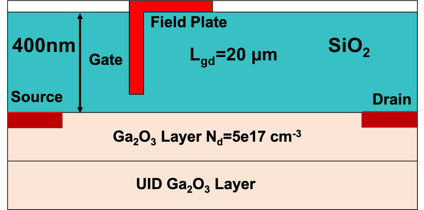
Fig 1 shows the device structure of the baseline Ga2O3 MOSFET. The channel layer is 200 nm thick with a doping concentration of 51017 cm-3. The ohmic layers, used for the drain and source contacts are 50 nm thick and heavily doped with a concentration of 11019 cm-3. The gate electrode has a work function of 4.8 eV. Field plate edge termination technique Sharma et al. (2020); Zeng, Vaidya, and Singisetti (2019) is used to maximize the breakdown voltage of the device. The device was simulated using the 2-D simulator of SILVACO ATLAS. The models used in the simulation include the SRH recombination model, Auger recombination model, impact ionization model, and the field dependent mobility model. According to previous studies from first principle calculationsGhosh and Singisetti (2016, 2017) the low field mobility of Ga2O3 is taken to be 150 cm2/V-s for a doping concentration of 51017 cm-3. The hole mobility in the channel is taken to be 0.1 cm2/V-s which is quite low due to the weakly interacting O 2p states which create deep acceptors. The impact ionization parameters for -Ga2O3 have been taken from a detailed first principle theoretical studyGhosh and Singisetti (2018).
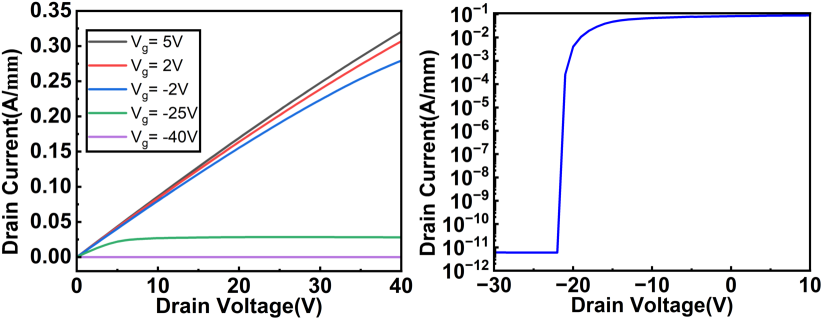
Fig. 2 shows the output and transfer characteristics of the device. The threshold voltage of the device from Fig. 2 is -20 V.
The breakdown voltage of the device is determined by analyzing the electric field contour plots at specified operating bias. Fig. 3 shows the electric field profile at the breakdown voltage of the device.
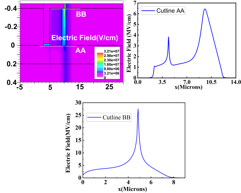
The device breakdown is determined when the electric field in the channel exceeds the critical breakdown field of SiO2 and Ga2O3. As shown in Fig. 3 at 1500 V, the field in the channel is close to 7 MV/cm and that of SiO2 is 25 MV/cm which is close to their critical breakdown fields. Thus the breakdown voltage of the device is estimated to be 1500V, which is close to the experimentally reported breakdown voltage Sharma et al. (2020); Zeng, Vaidya, and Singisetti (2019) at comparable gate-drain spacing.
III Single Event Effects
Single Event Effects (SEE) occur when individual energetic particle induces errors or failures in the device or the overall circuitPetersen (2011); Witulski et al. (2018); Khachatrian et al. (2016). The incident ionization particle loses energy in the semiconductor through Coulomb interaction with the lattice structure. The energy is transferred to the lattice as an ionization tail of free electron-hole pairs leading to transient current. Under heavy ion radiation conditions, a second breakdown mechanism might occur leading to a catastrophic failure of the device known as Single Event Burnout (SEB).
In radiation studies, a common measure of the loss of energy of the SEU particle, as it suffers collisions in a material, is the linear energy transfer (LET) value, which is given in units of MeV/mg/cm2. LET is the linear energy transfer of the incident ion which determines the number of electron hole pairs (ehp) created in the material depending on the band structure and the density of the material. The creation energy of an electron-hole pair in the semiconductor() is approximately calculated to be three times the band gap of the materialAlig and Bloom (1975). The number of free carriers released is calculated asWeatherford (2003):
| (1) |
The amount of electron-hole pairs created by the ionizing particle can be converted in terms of the linear charge deposited inside the semiconductor in units of pC/m. Since Ga2O3 is a wide band gap semiconductor, the conversion factor for material comes to be 0.007 pC/m corresponding to LET= 1 MeV/mg/cm2. This is quite low compared to 0.1 pC/m for Si and is comparable to other wide band gap materials like GaN and SiC. Thus the lower charge deposition by the ionizing particle and the highly promising properties Ga2O3 based devices might provide better radiation tolerance than other wide band gap materials.
The single event effects can be simulated using the ATLAS 2D simulator by using the SINGLEEVENTUPSET statement. The radius, length, and time dependence of the charge generation track can be specified. The coordinates of the entry and exit points of the track can also be specified within the device. In 2D simulations, the track is assumed to be a cylinder with a specified radius. The electron/hole pairs generated at any point are a function of the radial distance r, from the center of the track to the point, the distance l along the track, and the time, t. ATLAS implements the generation rate as the number of electron-hole pairs per along the track according to the equation:
where DENSITY and B.DENSITY are defined as the number of generated electron/hole pairs per cm-3. By setting a PCUNITS parameter, we can specify the charge generated in terms of pC/ depending on the LET value of the ionizing radiation and the concerned semiconductor as discussed above. The factors L1 and L2 define the variation of charger or carrier generation along the SEU track. The factor R(r) is the radial parameter and is defined as:
| (2) |
The factor T(t) is the time dependency of the charge generation governed by two user-defined parameters namely the temporal Gaussian function width and the initial time of charge generation.
IV SEE Simulations
The single event effects in Ga2O3 MOSFETs are investigated using the single event upset model in SILVACO TCAD. In accordance with the previous radiation research studiesBall et al. (2019); Luo et al. (2019), the spatial Gaussian function width is set to 50 nm, the temporal Gaussian function width is set to 2 ps, and the initial time of charge generation is set to 100 ps. The strike location is chosen by studying the electric field profile of the device before radiation. As shown in Fig. 2b, the location in the channel vertically under the edge of the field plate has a very high peak electric field and thus is the most sensitive region for SEE events following an ion strike. Thermal simulation models are also included but our analysis suggests that the temperature of the device stays within the tolerance limits. The simulation parameters along with the device parameters are shown in Table. 1.
| Design Parameters | Value |
|---|---|
| Lgd(Gate to Drain Length) | 20 |
| Thickness of dielectric | 400 nm |
| Channel Layer doping | 517 cm-3 |
| Dielectric constant of SiO2 | 3.9 |
| Dielectric constant of HfO2 | 25 |
| Dielectric constant of BaTiO3 | 100 |
| Spatial Gaussian function width | 50 nm Ball et al. (2019); Luo et al. (2019) |
| Temporal Gaussian function width | 210-12s Ball et al. (2019); Luo et al. (2019) |
| Initial Time of of charge generation | 100e-12 Ball et al. (2019); Luo et al. (2019) |
| Length of ion track | 10,0 - 10,0.4 |
| Hole recombination time | 410-10s |
| Models used | auger, srh, fldmob, impact,lat.temp |
| Impact Ionization Parameters. | a=0.79106, b=2.92107 Ghosh and Singisetti (2018) |
The MOSFET structure shown in Fig. 1 was simulated under two operating biases and LET=10 MeV/mg/cm2 to understand the SEE effects. From Fig. 4 it can be seen that there is a peak transient current for both conditions just after the ion strike, but with time it slowly recovers. However, at Vds= 500 V, a second breakdown mechanism occurs which is discussed below, the current starts to increase and goes beyond the safety limits. Thus the device recovers under Vds=220 V but suffers from SEB at Vds=500 V at LET=10 MeV/mg/cm2.
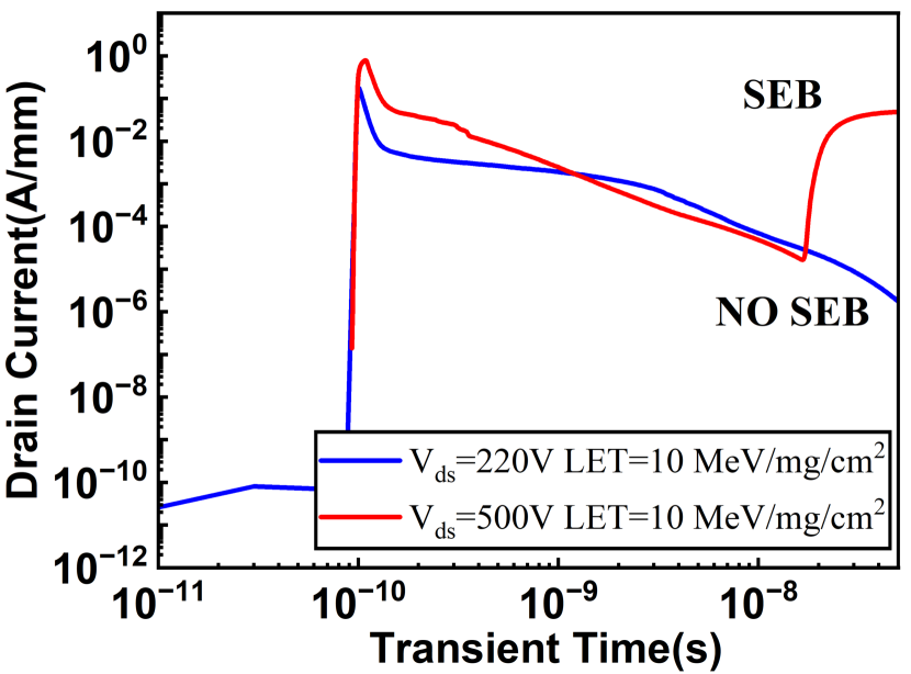
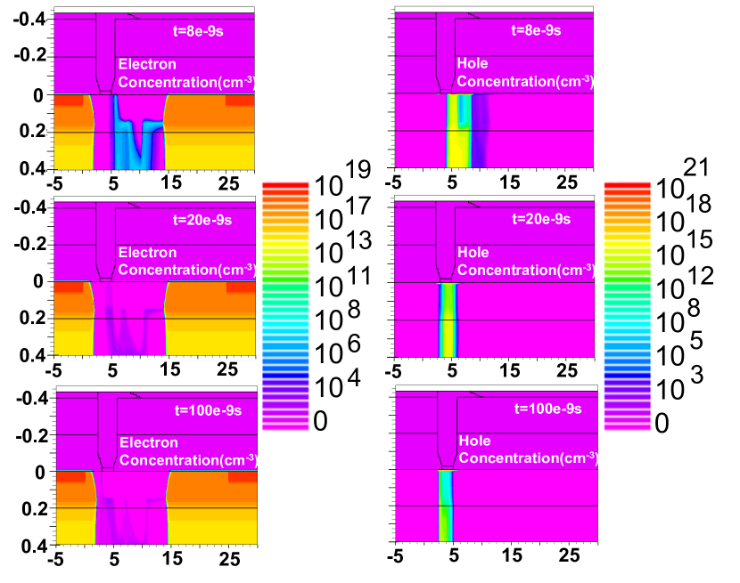
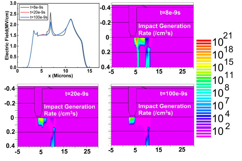
The physics behind the SEB failure can be understood by analyzing the electron, hole concentration profiles, and electric field contour at various time instants. Fig. 5 and Fig. 6 show the electron and hole concentration respectively in the device at various time instants after the ion strike. At t=1.0410-10s, which is just after the ion strike, electron-hole pairs are generated along the ion strike path as shown in Fig. 5a and Fig. 6a. Gradually with time, the electrons start to migrate towards the drain and the holes start to migrate towards the gate which is shown in Fig. 5b and Fig. 6b. Now as shown in Fig. 7a, the electric field in the channel is high with peaks under the gate and at the ion strike path. With time as more and more carriers start to accumulate near the gate, the impact generation rate starts to increase gradually. As shown in Fig. 7, initially the impact generation rate was present only under the ion strike path. But with time as more and more holes and electrons started accumulating under the gate, the impact generation rate increased which leads to high electron and hole concentration in the channel at t=8 onwards. At t=15, the impact generation rate is very high generating a huge concentration of electrons and holes as shown in Fig. 6d and Fig. 7d which are present throughout the channel. This leads to the SEB failure with current exceeding the safety limits of 1 mA/mm,Liu et al. (2022) as shown in Fig. 4.
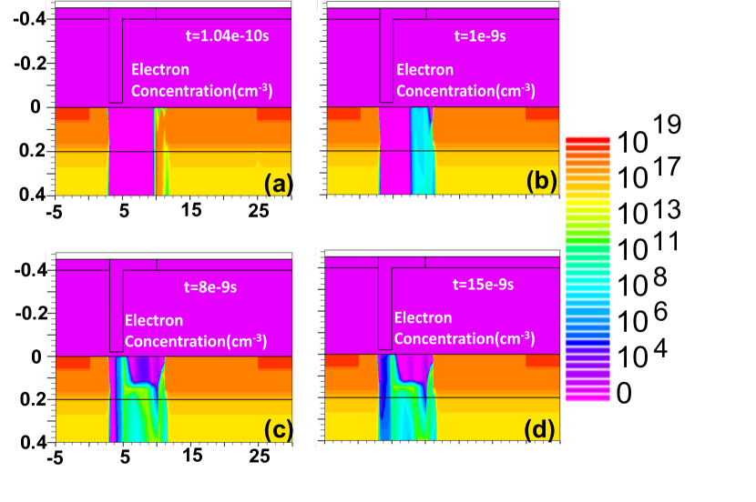
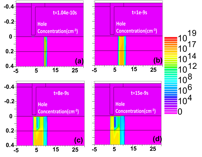
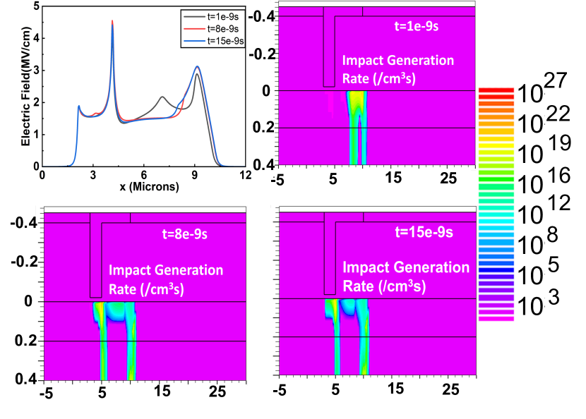
Thus with the baseline design the SEB threshold of 220 V at LET=10 MeV/mg/cm2 for the Ga2O3 MOSFET is lower than simulated SEB in radiation hardened GaN HEMTsLiu et al. (2022) and AlGaN/GaN-Based MISFETLuo et al. (2019).
The mechanism discussed above clearly indicates that the electric field in the channel should be reduced to design radiation hardened MOSFETs. Thus a modified design with a high-k dielectric combination is proposed here.
V Radiation hardened design
As discussed in the earlier section, to reduce the overall electric field in the channel, a MOSFET design with a combination of high-k dielectric and SiO2 as shown in Fig. 8 is proposed.
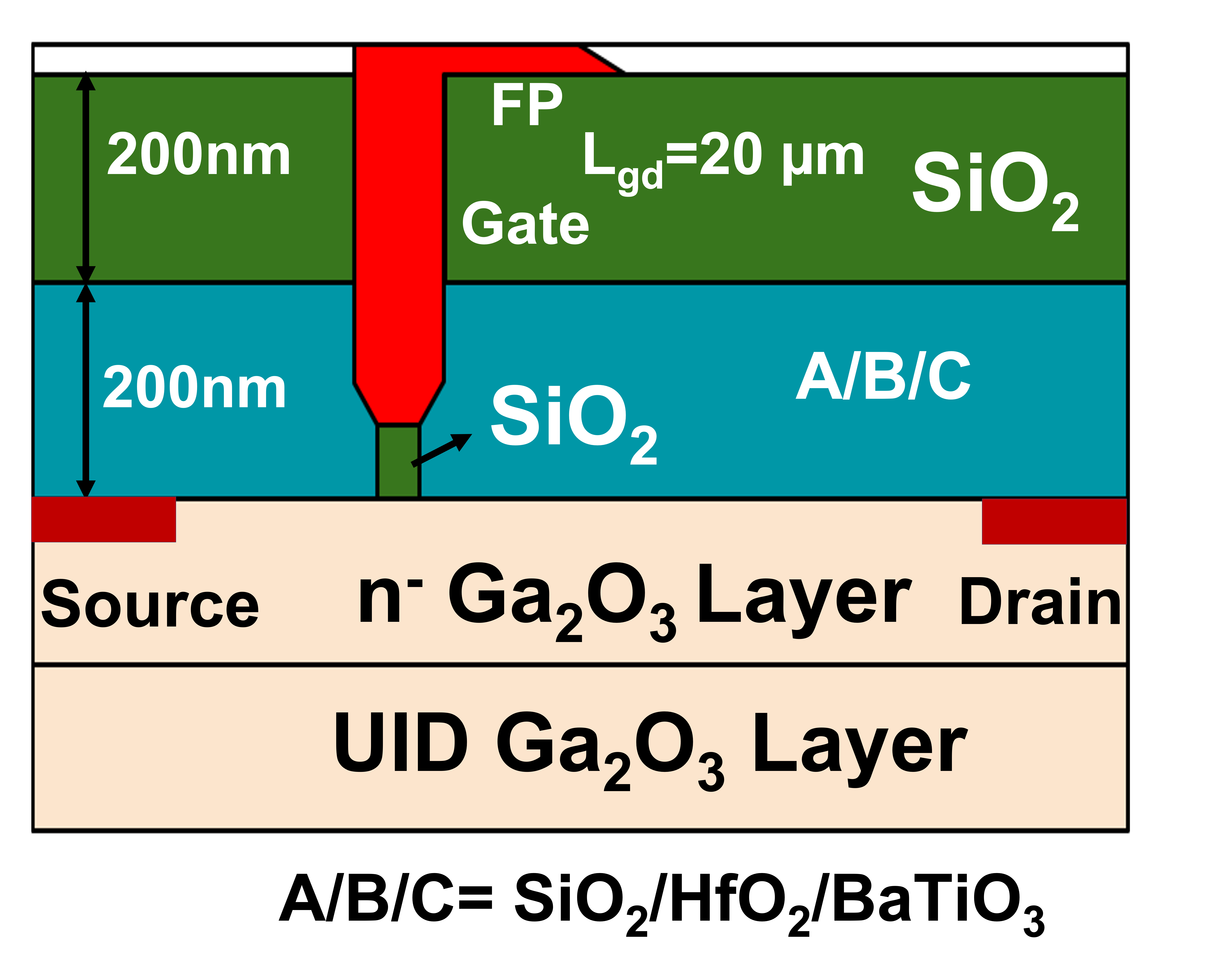
The first design is proposed with the combination of conventional dielectrics which is HfO2 and SiO2. However, due to possible band alignment issues with Ga2O3 and HfO2, the gate dielectric has been kept SiO2. Gate rounding techniques have also been implemented to reduce the electric field crowding at the edges and also mimic the simulation as closely as possible to a fabricated structure.
The structure was simulated under two radiation condition of Vds=550 V and LET=10 MeV/mg/cm2 and Vds=650 V and LET= 75 MeV/mg/cm2
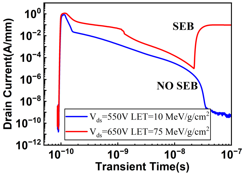
At Vds=550 V and LET=10 MeV/mg/cm2, the current recovers, and the leakage current is still within the safe limits indicating that the device has not suffered SEB. To understand how the proposed design helps in increasing the SEB threshold at LET=10 MeV/mg/cm2, it is important to look at the electron, hole concentrations, and the impact generation rate at various time instants. During the initial period of ion strike, the electrons and holes behave similarly to as discussed in the earlier section. There is a peak transient current just after the ion strike as shown in Fig. 9 and then for both cases, the current starts to recover slowly. However as shown in Fig. 11a, the electric field in the channel is lower especially under the gate as compared to the conventional structure though the device is operating at a higher bias. Thus at t=1010-9s, the impact generation rate is significantly lower leading to lower levels of electron and hole concentration as shown in Fig. 10. As a result, the drain current does increase again. The current stays below the safety limits and SEB is not triggered.
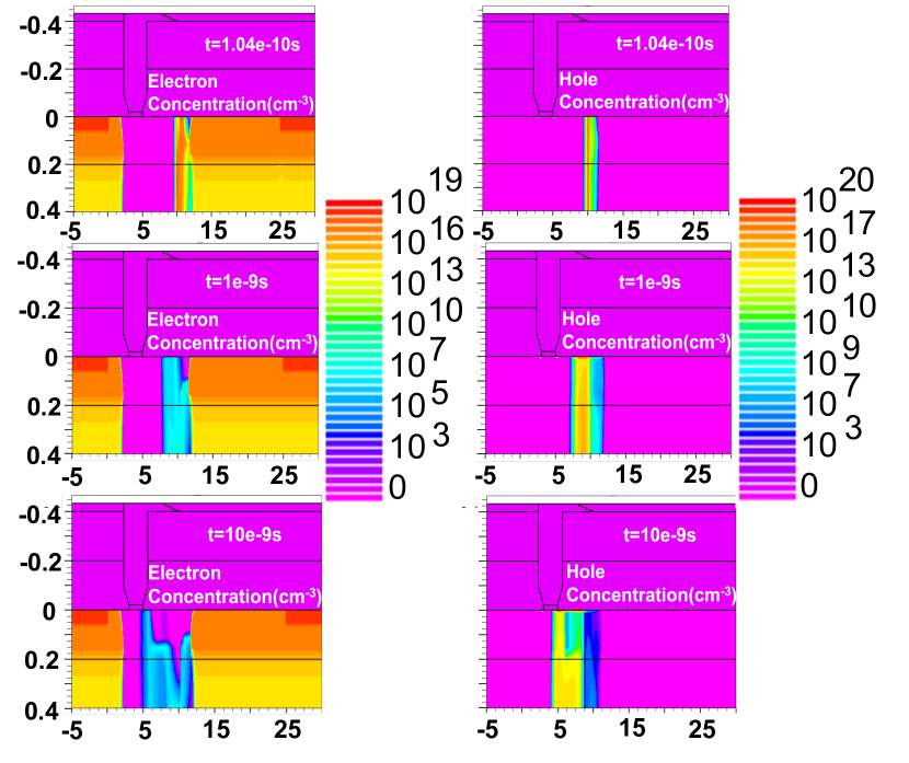
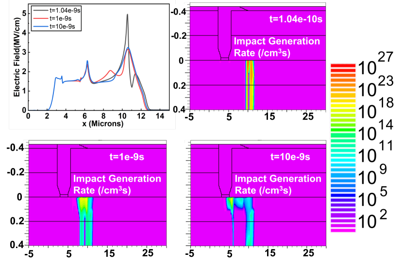
However, for extreme radiation conditions of Vds=650 V and LET=75 MeV/mg/cm2, the device suffers from SEB because the impact generation rate becomes higher due to higher electric fields in the channel. Thus to get further radiation hardness, a very high-k dielectric material has to be used.
Here we have proposed a combination of BaTiO3 and SiO2 as shown in Fig. 8. Fig. 12 and Fig. 13 shows the transient drain current plots under radiation conditions of Vds=650 V LET=75 MeV/mg/cm2 and Vds=1000 V LET=75 MeV/mg/cm2 respectively.
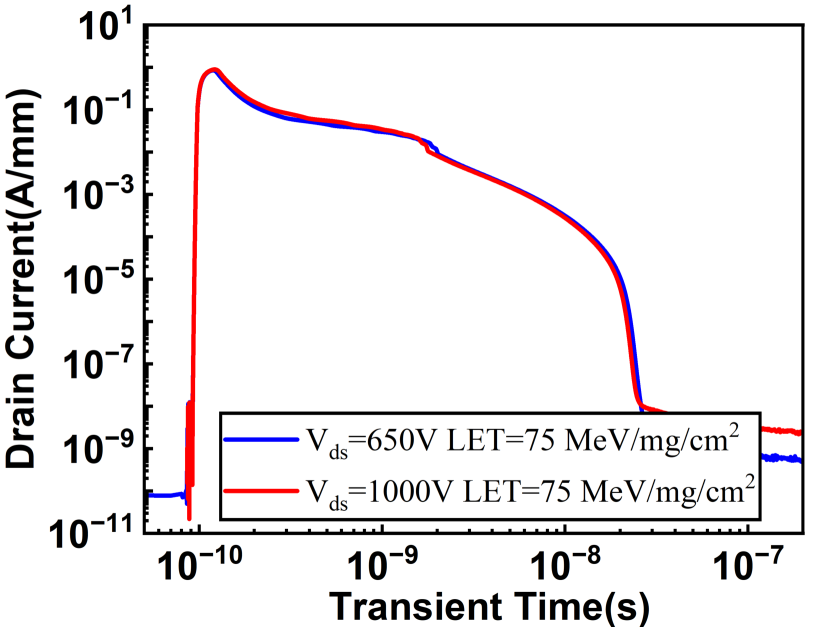
The device shows full current recovery which can be further understood by analyzing the electron, hole, and impact generation rate contour plots at various time instants. As shown in Fig. 14, the electric field is significantly lowered even at a high operating bias of 1000 V, which leads to low impact generation rates in the channel. The electron and hole concentration is shown from t=810-9s onwards since before that the behavior of electrons and holes is similar to the earlier cases. Thus even though carriers are present in the channel at 810-9s, they start to recombine with each other instead of undergoing impact ionization. The result is clearly seen in Fig. 13 where the electron and hole concentration is very low as time progresses. Therefore the drain current does not increase with time, and the device is immune to extreme radiation conditions.
Ideally, if a high-k dielectric like HfO2 or BaTiO3 of higher thickness could be used as a fully dielectric layer for the MOSFET, the radiation hardness could be increased further. However high leakage currents and challenges of depositing thick dielectrics limit us in using that design.
To further verify our simulations, we have also varied the hole mobility to 2 cm2V-1s-1Ma et al. (2022) and have obtained similar results which shows that the hole mobility is not an important factor for determining the SEB threshold condition.
VI Energy dissipation calculation
The amount of energy dissipated during the ionizing radiation event in the MOSFET is an important factor in analyzing the radiation hardness of the semiconductor material. The energy dissipated during each event can be calculated by integrating the current density times area of ion track and the electric field along the entire ion track and then integrating temporally. The area of the ion track is taken to be r2, where r is the radius of the ion track. The energy dissipated is calculated using the following equationBall et al. (2019)
| (3) |
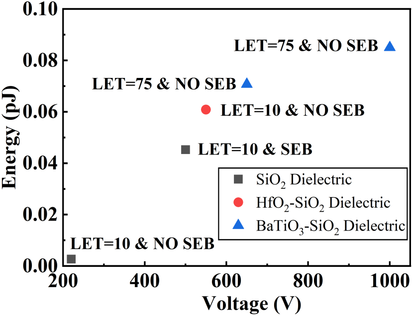
Fig.15 shows the energy dissipated for the first 336ps of the ion strike event in -Ga2O3 MOSFETs under different radiation conditions. It is observed that the power dissipated for ion strike event in Ga2O3 MOSFET irrespective of the radiation condition is significantly less than that energy dissipated in SiC MOSFETsBall et al. (2019). This results from the lower ionization rate in Ga2O3 due to its large bandgap. The energy dissipated increases with increasing LET and increasing operating bias which is in accordance with our discussion in the earlier sections that with increasing bias and LET, the electric fields could be higher and the transient drain current peaks are higher. However, the energy dissipation factor is not correlated with specific SEB effect as seen in the figure.
VII Peak Electric Field and SEB Threshold condition
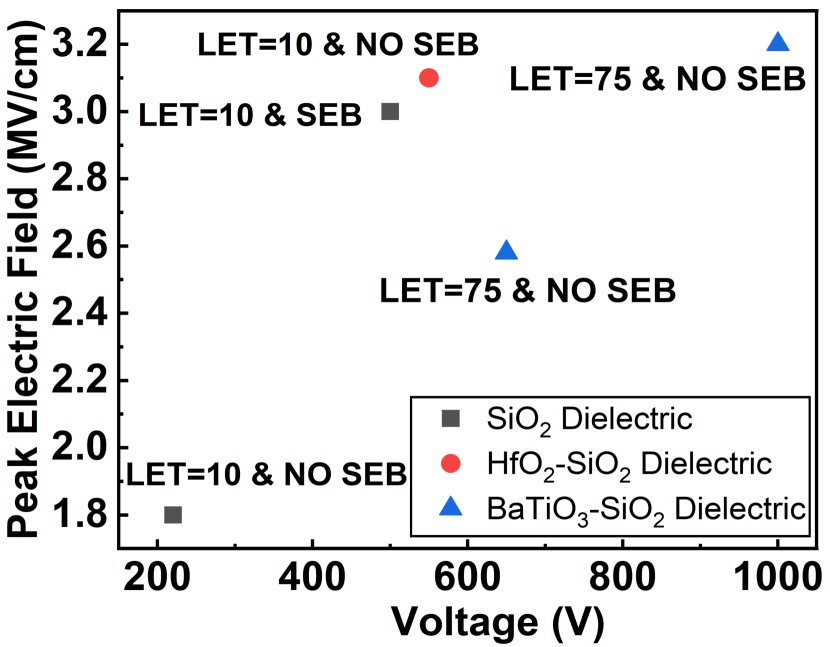
As discussed in the earlier section, though the energy dissipation in Ga2O3 MOSFET is lower than that of SiC MOSFETs, it is not a helpful parameter in determining a specific SEB threshold condition for voltage or LET. The main factor responsible for triggering the SEB mechanism was found to be the electric field. Though our simulations suggest that decreasing the electric field in the channel increases the SEB threshold conditions, it is difficult to identify a specific threshold condition that is applicable for Ga2O3 MOSFETs across all design modifications. Fig. 16 shows the variation of peak electric field in the channel at the location of ion strike at t=810-9s for all the designs. It can be clearly seen that using a high-k dielectric reduces the peak electric fields in the channel but it also changes the overall electric field distribution in the device. But the peak electric field value is not the decisive factor for determining the SEB triggering mechanism. The overall electric field distribution affects the total impact generation rate in the device which is responsible for the generation of carriers. For example, if we take radiation condition of Vds=500 V and LET=10 MeV/mg/cm2 for the conventional design shown in Fig. 1 and a radiation condition of Vds=1000 V and LET=75 MeV/mg/cm2 for the modified design shown in Fig. 8 with the BaTiO3 dielectric, the peak electric fields in the channel for the BaTiO3-SiO2 design is higher as shown in Fig. 16. However, the field distributions are different for the two designs, which leads to different impact generation rates and different levels of electron and hole concentrations as discussed earlier. Thus even though the peak electric field value is higher the BaTiO3-SiO2 design combination does not suffer from SEB, whereas in the SiO2 design, SEB is triggered.
VIII Conclusion
In this article, detailed 2D TCAD simulations were performed to investigate the SEEs in -Ga2O3 MOSFETs. The physics behind the SEB mechanism is understood and the electric field distribution in the channel is one of the main factors behind the SEB triggering mechanism. Our initial simulations suggest that the SEB threshold voltage of the baseline lateral Ga2O3 MOSFET is lower than the simulated SEB threshold in state of the art AlGaN/GaN HEMTs and MISFETs. Thus keeping in mind the physics behind the SEB mechanism radiation hardening techniques are proposed which show improved radiation hardened performance. To reduce the high electric fields in the channel responsible for the high impact generation rates, a radiation hardened device with rounded gates and high-k dielectric was proposed. The high-k dielectric is used in combination with SiO2 to reduce the fabrication challenges associated with depositing a thick layer of high-k dielectric. Firstly, with HfO2-SiO2 dielectric combination, SEB threshold voltage of 550V is obtained which is higher than that of GaN HEMTs. However, this design also fails under extreme radiation conditions. Therefore it is proposed that to operate under extreme radiation conditions, a very high-k dielectric material like BaTiO3 could be used which reduces the overall electric field distribution in the channel significantly. With this design, the device can achieve SEB thresholds going up to 1000V at LET=75 MeV/mg/cm2. Another technique that could be explored to design radiation hardened -Ga2O3 MOSFETs, is using a p-type material like p-NiO, which is also helpful in reducing the electric field in the channel.
Acknowledgements.
We acknowledge the support from AFOSR under award FA9550-18-1-0479 (Program Manager: Ali Sayir), from NSF under awards ECCS 2019749, ECCS 2231026References
- Srour and Palko (2006) J. Srour and J. Palko, “A framework for understanding displacement damage mechanisms in irradiated silicon devices,” IEEE transactions on nuclear science 53, 3610–3620 (2006).
- Dodds et al. (2015) N. A. Dodds, M. J. Martinez, P. E. Dodd, M. R. Shaneyfelt, F. W. Sexton, J. D. Black, D. S. Lee, S. E. Swanson, B. Bhuva, K. Warren, et al., “The contribution of low-energy protons to the total on-orbit seu rate,” IEEE Transactions on Nuclear Science 62, 2440–2451 (2015).
- Martinez et al. (2018) M. Martinez, M. P. King, A. G. Baca, A. A. Allerman, A. A. Armstrong, B. A. Klein, E. A. Douglas, R. J. Kaplar, and S. E. Swanson, “Radiation response of algan-channel hemts,” IEEE Transactions on Nuclear Science 66, 344–351 (2018).
- Kim et al. (2019) J. Kim, S. J. Pearton, C. Fares, J. Yang, F. Ren, S. Kim, and A. Y. Polyakov, “Radiation damage effects in ga 2 o 3 materials and devices,” Journal of Materials Chemistry C 7, 10–24 (2019).
- Look et al. (1997) D. C. Look, D. Reynolds, J. W. Hemsky, J. Sizelove, R. Jones, and R. J. Molnar, “Defect donor and acceptor in gan,” Physical review letters 79, 2273 (1997).
- Ionascut-Nedelcescu et al. (2002) A. Ionascut-Nedelcescu, C. Carlone, A. Houdayer, H. Von Bardeleben, J.-L. Cantin, and S. Raymond, “Radiation hardness of gallium nitride,” IEEE Transactions on Nuclear Science 49, 2733–2738 (2002).
- Barry et al. (1991) A. Barry, B. Lehmann, D. Fritsch, and D. Braunig, “Energy dependence of electron damage and displacement threshold energy in 6h silicon carbide,” IEEE transactions on nuclear science 38, 1111–1115 (1991).
- Witulski et al. (2017) A. Witulski, R. Arslanbekov, A. Raman, R. Schrimpf, A. Sternberg, K. Galloway, A. Javanainen, D. Grider, D. Lichtenwalner, and B. Hull, “Single-event burnout of sic junction barrier schottky diode high-voltage power devices,” IEEE Transactions on Nuclear Science 65, 256–261 (2017).
- Li et al. (2021) M.-B. Li, F. Cao, H.-F. Hu, X.-J. Li, J.-Q. Yang, and Y. Wang, “High single-event burnout resistance 4h-sic junction barrier schottky diode,” IEEE Journal of the Electron Devices Society 9, 591–598 (2021).
- McPherson et al. (2018) J. A. McPherson, P. J. Kowal, G. K. Pandey, T. P. Chow, W. Ji, and A. A. Woodworth, “Heavy ion transport modeling for single-event burnout in sic-based power devices,” IEEE Transactions on Nuclear Science 66, 474–481 (2018).
- Javanainen et al. (2016) A. Javanainen, K. F. Galloway, C. Nicklaw, A. L. Bosser, V. Ferlet-Cavrois, J.-M. Lauenstein, F. Pintacuda, R. A. Reed, R. D. Schrimpf, R. A. Weller, et al., “Heavy ion induced degradation in sic schottky diodes: Bias and energy deposition dependence,” IEEE Transactions on Nuclear Science 64, 415–420 (2016).
- Mizuta et al. (2014) E. Mizuta, S. Kuboyama, H. Abe, Y. Iwata, and T. Tamura, “Investigation of single-event damages on silicon carbide (sic) power mosfets,” IEEE Transactions on Nuclear Science 61, 1924–1928 (2014).
- Makino et al. (2013) T. Makino, M. Deki, N. Iwamoto, S. Onoda, N. Hoshino, H. Tsuchida, T. Hirao, and T. Ohshima, “Heavy-ion induced anomalous charge collection from 4h-sic schottky barrier diodes,” IEEE Transactions on Nuclear Science 60, 2647–2650 (2013).
- Kuboyama et al. (2006) S. Kuboyama, C. Kamezawa, N. Ikeda, T. Hirao, and H. Ohyama, “Anomalous charge collection in silicon carbide schottky barrier diodes and resulting permanent damage and single-event burnout,” IEEE transactions on nuclear science 53, 3343–3348 (2006).
- Ball et al. (2019) D. Ball, K. Galloway, R. Johnson, M. Alles, A. Sternberg, B. Sierawski, A. Witulski, R. Reed, R. Schrimpf, J. Hutson, et al., “Ion-induced energy pulse mechanism for single-event burnout in high-voltage sic power mosfets and junction barrier schottky diodes,” IEEE Transactions on Nuclear Science 67, 22–28 (2019).
- Pearton, Hwang, and Ren (2015) S. Pearton, Y.-S. Hwang, and F. Ren, “Radiation effects in gan-based high electron mobility transistors,” Jom 67, 1601–1611 (2015).
- Lee et al. (2017) I.-H. Lee, A. Polyakov, E. Yakimov, N. Smirnov, I. Shchemerov, S. Tarelkin, S. Didenko, K. Tapero, R. Zinovyev, and S. Pearton, “Defects responsible for lifetime degradation in electron irradiated n-gan grown by hydride vapor phase epitaxy,” Applied Physics Letters 110, 112102 (2017).
- Yadav et al. (2015) A. Yadav, E. Flitsiyan, L. Chernyak, Y.-H. Hwang, Y.-L. Hsieh, L. Lei, F. Ren, S. J. Pearton, and I. Lubomirsky, “Low and moderate dose gamma-irradiation and annealing impact on electronic and electrical properties of algan/gan high electron mobility transistors,” Radiation Effects and Defects in Solids 170, 377–385 (2015).
- Patrick et al. (2015) E. E. Patrick, M. Choudhury, F. Ren, S. J. Pearton, and M. E. Law, “Simulation of radiation effects in algan/gan hemts,” ECS Journal of Solid State Science and Technology 4, Q21 (2015).
- Liu et al. (2022) S. Liu, J. Zhang, S. Zhao, L. Shu, X. Song, X. Qin, Y. Wu, W. Zhang, T. Li, L. Wang, et al., “Simulation research on single event burnout performances of p-gan gate hemts with 2deg alxga1-xn channel,” IEEE Transactions on Electron Devices 69, 973–980 (2022).
- Luo et al. (2019) X. Luo, Y. Wang, Y. Hao, X.-j. Li, C.-M. Liu, X.-X. Fei, C.-H. Yu, and F. Cao, “Research of single-event burnout and hardening of algan/gan-based misfet,” IEEE Transactions on Electron Devices 66, 1118–1122 (2019).
- Tsao et al. (2018) J. Tsao, S. Chowdhury, M. Hollis, D. Jena, N. Johnson, K. Jones, R. Kaplar, S. Rajan, C. Van de Walle, E. Bellotti, et al., “Ultrawide-bandgap semiconductors: research opportunities and challenges,” Advanced Electronic Materials 4, 1600501 (2018).
- Tadjer et al. (2016) M. J. Tadjer, M. A. Mastro, N. A. Mahadik, M. Currie, V. D. Wheeler, J. A. Freitas, J. D. Greenlee, J. K. Hite, K. D. Hobart, C. R. Eddy, et al., “Structural, optical, and electrical characterization of monoclinic -ga2o3 grown by movpe on sapphire substrates,” Journal of Electronic Materials 45, 2031–2037 (2016).
- Baldini et al. (2016) M. Baldini, M. Albrecht, A. Fiedler, K. Irmscher, R. Schewski, and G. Wagner, “Si-and sn-doped homoepitaxial -ga2o3 layers grown by movpe on (010)-oriented substrates,” ECS Journal of Solid State Science and Technology 6, Q3040 (2016).
- Galazka et al. (2016) Z. Galazka, R. Uecker, D. Klimm, K. Irmscher, M. Naumann, M. Pietsch, A. Kwasniewski, R. Bertram, S. Ganschow, and M. Bickermann, “Scaling-up of bulk -ga2o3 single crystals by the czochralski method,” ECS Journal of Solid State Science and Technology 6, Q3007 (2016).
- Stepanov et al. (2016) S. Stepanov, V. Nikolaev, V. Bougrov, and A. Romanov, “Gallium oxide: Properties and applica 498 a review,” Rev. Adv. Mater. Sci 44, 63–86 (2016).
- Bhattacharyya et al. (2021) A. Bhattacharyya, P. Ranga, S. Roy, C. Peterson, F. Alema, G. Seryogin, A. Osinsky, and S. Krishnamoorthy, “Multi-kv class -ga2o3 mesfets with a lateral figure of merit up to 355 mw/cm²,” IEEE Electron Device Letters 42, 1272–1275 (2021).
- Bhattacharyya et al. (2022) A. Bhattacharyya, S. Sharma, F. Alema, P. Ranga, S. Roy, C. Peterson, G. Seryogin, A. Osinsky, U. Singisetti, and S. Krishnamoorthy, “4.4 kv -ga2o3 mesfets with power figure of merit exceeding 100 mw cm- 2,” Applied Physics Express 15, 061001 (2022).
- Sharma et al. (2020) S. Sharma, K. Zeng, S. Saha, and U. Singisetti, “Field-plated lateral ga 2 o 3 mosfets with polymer passivation and 8.03 kv breakdown voltage,” IEEE Electron Device Letters 41, 836–839 (2020).
- Zeng, Vaidya, and Singisetti (2019) K. Zeng, A. Vaidya, and U. Singisetti, “A field-plated ga2o3 mosfet with near 2-kv breakdown voltage and 520 m· cm2 on-resistance,” Applied Physics Express 12, 081003 (2019).
- Mun et al. (2019) J. K. Mun, K. Cho, W. Chang, H.-W. Jung, and J. Do, “2.32 kv breakdown voltage lateral -ga2o3 mosfets with source-connected field plate,” ECS Journal of Solid State Science and Technology 8, Q3079 (2019).
- Chabak et al. (2016) K. D. Chabak, N. Moser, A. J. Green, D. E. Walker Jr, S. E. Tetlak, E. Heller, A. Crespo, R. Fitch, J. P. McCandless, K. Leedy, et al., “Enhancement-mode ga2o3 wrap-gate fin field-effect transistors on native (100) -ga2o3 substrate with high breakdown voltage,” Applied Physics Letters 109, 213501 (2016).
- Lv et al. (2020) Y. Lv, H. Liu, X. Zhou, Y. Wang, X. Song, Y. Cai, Q. Yan, C. Wang, S. Liang, J. Zhang, et al., “Lateral -ga 2 o 3 mosfets with high power figure of merit of 277 mw/cm 2,” IEEE Electron Device Letters 41, 537–540 (2020).
- Li et al. (2018) W. Li, K. Nomoto, Z. Hu, N. Tanen, K. Sasaki, A. Kuramata, D. Jena, and H. G. Xing, “1.5 kv vertical ga 2 o 3 trench-mis schottky barrier diodes,” in 2018 76th Device Research Conference (DRC) (IEEE, 2018) pp. 1–2.
- Schubert et al. (2020) M. Schubert, A. Mock, R. Korlacki, S. Knight, B. Monemar, K. Goto, Y. Kumagai, A. Kuramata, Z. Galazka, G. Wagner, et al., “Gallium oxide: materials properties, crystal growth, and devices,” (2020).
- Zhang et al. (2022) J. Zhang, P. Dong, K. Dang, Y. Zhang, Q. Yan, H. Xiang, J. Su, Z. Liu, M. Si, J. Gao, et al., “Ultra-wide bandgap semiconductor ga2o3 power diodes,” Nature communications 13, 1–8 (2022).
- Roy et al. (2022) S. Roy, A. Bhattacharyya, C. Peterson, and S. Krishnamoorthy, “-ga2o3 lateral high-permittivity dielectric superjunction schottky barrier diode with 1.34 gw/cm² power figure of merit,” IEEE Electron Device Letters 43, 2037–2040 (2022).
- Roy et al. (2021) S. Roy, A. Bhattacharyya, P. Ranga, H. Splawn, J. Leach, and S. Krishnamoorthy, “High-k oxide field-plated vertical (001) -ga2o3 schottky barrier diode with baliga’s figure of merit over 1 gw/cm2,” IEEE Electron Device Letters 42, 1140–1143 (2021).
- Wong et al. (2018) M. H. Wong, A. Takeyama, T. Makino, T. Ohshima, K. Sasaki, A. Kuramata, S. Yamakoshi, and M. Higashiwaki, “Radiation hardness of -ga2o3 metal-oxide-semiconductor field-effect transistors against gamma-ray irradiation,” Applied Physics Letters 112, 023503 (2018).
- Lingaparthi et al. (2019) R. Lingaparthi, K. Sasaki, Q. T. Thieu, A. Takatsuka, F. Otsuka, S. Yamakoshi, and A. Kuramata, “Surface related tunneling leakage in -ga2o3 (001) vertical schottky barrier diodes,” Applied Physics Express 12, 074008 (2019).
- Polyakov et al. (2022) A. Y. Polyakov, V. I. Nikolaev, E. B. Yakimov, F. Ren, S. J. Pearton, and J. Kim, “Deep level defect states in -, -, and -ga2o3 crystals and films: Impact on device performance,” Journal of Vacuum Science & Technology A: Vacuum, Surfaces, and Films 40, 020804 (2022).
- Yakimov et al. (2021) E. Yakimov, A. Polyakov, I. Shchemerov, N. Smirnov, A. Vasilev, P. Vergeles, E. Yakimov, . A. Chernykh, F. Ren, and S. Pearton, “Experimental estimation of electron–hole pair creation energy in -ga2o3,” Applied Physics Letters 118, 202106 (2021).
- Xia et al. (2019) Z. Xia, H. Chandrasekar, W. Moore, C. Wang, A. J. Lee, J. McGlone, N. K. Kalarickal, A. Arehart, S. Ringel, F. Yang, et al., “Metal/batio3/-ga2o3 dielectric heterojunction diode with 5.7 mv/cm breakdown field,” Applied Physics Letters 115, 252104 (2019).
- Razzak et al. (2020) T. Razzak, H. Chandrasekar, K. Hussain, C. H. Lee, A. Mamun, H. Xue, Z. Xia, S. H. Sohel, M. W. Rahman, S. Bajaj, et al., “Batio3/al0. 58ga0. 42n lateral heterojunction diodes with breakdown field exceeding 8 mv/cm,” Applied Physics Letters 116, 023507 (2020).
- Rahman et al. (2021) M. W. Rahman, N. K. Kalarickal, H. Lee, T. Razzak, and S. Rajan, “Integration of high permittivity batio3 with algan/gan for near-theoretical breakdown field kv-class transistors,” Applied Physics Letters 119, 193501 (2021).
- Ghosh and Singisetti (2016) K. Ghosh and U. Singisetti, “Ab initio calculation of electron–phonon coupling in monoclinic -ga2o3 crystal,” Applied Physics Letters 109, 072102 (2016).
- Ghosh and Singisetti (2017) K. Ghosh and U. Singisetti, “Electron mobility in monoclinic -ga2o3—effect of plasmon-phonon coupling, anisotropy, and confinement,” Journal of Materials Research 32, 4142–4152 (2017).
- Ghosh and Singisetti (2018) K. Ghosh and U. Singisetti, “Impact ionization in -ga2o3,” Journal of Applied Physics 124, 085707 (2018).
- Petersen (2011) E. Petersen, Single event effects in aerospace (John Wiley & Sons, 2011).
- Witulski et al. (2018) A. F. Witulski, D. R. Ball, K. F. Galloway, A. Javanainen, J.-M. Lauenstein, A. L. Sternberg, and R. D. Schrimpf, “Single-event burnout mechanisms in sic power mosfets,” IEEE Transactions on Nuclear Science 65, 1951–1955 (2018).
- Khachatrian et al. (2016) A. Khachatrian, N.-H. Roche, S. P. Buchner, A. D. Koehler, T. J. Anderson, K. D. Hobart, D. McMorrow, S. D. LaLumondiere, N. Wells, J. Bonsall, et al., “Application of a focused, pulsed x-ray beam to the investigation of single-event transients in al 0.3 ga 0.7 n/gan hemts,” IEEE Transactions on Nuclear Science 64, 97–105 (2016).
- Alig and Bloom (1975) R. Alig and S. l. Bloom, “Electron-hole-pair creation energies in semiconductors,” Physical review letters 35, 1522 (1975).
- Weatherford (2003) T. R. Weatherford, “Radiation effects in high speed iii-v integrated circuits,” International journal of high speed electronics and systems 13, 277–292 (2003).
- Ma et al. (2022) C. Ma, Z. Wu, Z. Jiang, Y. Chen, W. Ruan, H. Zhang, H. Zhu, G. Zhang, J. Kang, T.-Y. Zhang, et al., “Exploring the feasibility and conduction mechanisms of p-type nitrogen-doped -ga 2 o 3 with high hole mobility,” Journal of Materials Chemistry C 10, 6673–6681 (2022).
- Sharma et al. (2019) R. Sharma, E. E. Patrick, M. Law, F. Ren, and S. Pearton, “Optimization of edge termination techniques for -ga2o3 schottky rectifiers,” ECS Journal of Solid State Science and Technology 8, Q234 (2019).