A Digital Delay Model Supporting Large Adversarial Delay Variations ††thanks: This research was supported by the Austrian Science Fund (FWF) project DMAC (grant no. P32431).
Abstract
Dynamic digital timing analysis is a promising alternative to analog simulations for verifying particularly timing-critical parts of a circuit. A necessary prerequisite is a digital delay model, which allows to accurately predict the input-to-output delay of a given transition in the input signal(s) of a gate. Since all existing digital delay models for dynamic digital timing analysis are deterministic, however, they cannot cover delay fluctuations caused by PVT variations, aging and analog signal noise. The only exception known to us is the -IDM introduced by Függer et al. at DATE’18, which allows to add (very) small adversarially chosen delay variations to the deterministic involution delay model, without endangering its faithfulness. In this paper, we show that it is possible to extend the range of allowed delay variations so significantly that realistic PVT variations and aging are covered by the resulting extended -IDM.
I Introduction
Accurate signal propagation predictions are crucial for modern digital circuit design. The highest accuracy is currently achievable by analog simulations, e.g., using SPICE. These suffer, however, from excessive running times. A considerably more efficient alternative is dynamic digital timing analysis, which traces individual signal transitions throughout a circuit. Application examples are clock trees or time-based encoded inter-neuron links in hardware-implemented spiking neural networks [1], where the (very accurate but worst-case) delay estimates provided by classic static timing analysis techniques like CCSM [2] and ECSM [3] are not sufficient for ensuring correct operation.
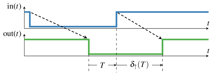
Existing digital dynamic timing analysis tools like Cadence NC-Sim, Siemens ModelSim or Synopsis VCS rely on simple gate delay models like pure delays (= constant delay) or inertial delays (= constant delay, but pulses shorter than some upper bound are removed) [4]. However, research has also provided more elaborate single-history delay models like the degradation delay model (DDM) [5] and, in particular, the involution delay model (IDM) [6, 7], where the input-to-output delay depends on the previous-output-to-input delay (see Fig. 1).
The distinguishing feature of the IDM is that it is the only delay model known so far that is faithful w.r.t. a “canonical” problem called short-pulse filtration (SPF) [8] (see Definition 1), which means that the solvability/impossibility border for circuits specified in the IDM matches the solvability/impossibility border for real circuits: whereas it is possible to implement unbounded SPF in reality, this is not the case for bounded SPF, where all output transitions must occur within bounded time. An essential property required for faithfulness is continuity of the underlying digital channel model, in the sense that minor changes (which also include short glitches, at arbitrary positions) of the signal at an input of a gate must result in minor changes of the output signal only. It has been proved in [8] that no existing delay model (except the IDM) satisfies this continuity property.
The defining characteristics of the IDM is a pair of differentiable concave delay functions (monotonically increasing, with monotonically decreasing derivative) for rising () and falling () transitions that satisfy the involution property . It has been proved in [7] that this ensures continuity and hence faithfulness w.r.t. the SPF problem. The IDM also comes with public domain tool support, the Involution Tool, a simulation framework based on ModelSim, which has been used to demonstrate the good accuracy of the IDM predictions for several simple circuits [9]. Certain deficiencies of the IDM regarding composition of circuits have been alleviated in the Composable Involution Delay Model (CIDM) [10].
One shortcoming of all existing delay models, including the original IDM and the CIDM, are their deterministic delay predictions. After all, e.g. is a function that only depends on the previous-output-to-input delay . Delay fluctuations caused by other effects, like PVT variations, aging, and electrical signal noise, cannot be accommodated here. Given the prominence of these effects in modern VLSI circuits, however, they should be incorporated somehow. We note that this requirement is even more pressing in any attempt on formal verification of circuits, which aims at proving that a given circuit will meet its specification in every feasible trace.
In their DATE’18 paper [11], Függer at. al. introduced an extension of the IDM, called -IDM, which allows to add a small amount of adversarial delay variations to the fully deterministic delay predictions of the IDM. That is, for every signal transition, the standard IDM delay can be replaced by for some arbitrarily chosen . This feature can of course be used to cover any bounded-range delay fluctuation. The authors proved that the resulting -IDM does not invalidate the faithfulness of the original IDM, provided the variation range is (very) small. Unfortunately, however, SPICE simulation data revealed that even voltage variations of 1 % and transistor size variations of 10 % already exceeded the allowed range.
In this paper, we show that the allowed range can be extended significantly. The key to our extended -IDM is to make the allowed variation range dependent on , i.e., to allow depending on the previous-output-to-input delay of the current transition. In particular, except for very small values of , the variation range may be large.
Detailed contributions
-
(1)
We define our extended -IDM, by providing the constraints that must be satisfied by , and prove that the SPF implementation already used in [11] also works correctly in this model.
- (2)
-
(3)
We perform elaborate analog simulations under different PVT variations and aging, and compare the simulated delays with the predicted delays of our -CIDM. It turns out that, unlike the model in [11], our new model can capture a wide range of such variations.
Paper organization
In Section II, the necessary basics for the IDM and the -IDM are presented. Section III provides the proofs for the faithfulness for the extended delay variation range. In Section IV, we sketch how the extended -IDM and the CIDM can be seamlessly combined. The experiments in Section V demonstrate the substantially increased coverage of our new model. Section VI concludes our paper.
II The Existing -IDM
In sharp contrast to all other delay models known so far, the IDM is based on unbounded single-history channels: Referring to Fig. 1, the gate delay may also become arbitrarily negative here (for specific values of the previous-output-to-input delay ), which has been proved to be mandatory for perfect glitch cancellation [8].
In order to also account for PVT variations and aging, [11] introduced the -IDM: On top of the deterministic delay calculations of the IDM, an adversarial delay is added. More specifically, the delay for the transition is calculated as
| (1) |
for a rising transition, and
| (2) |
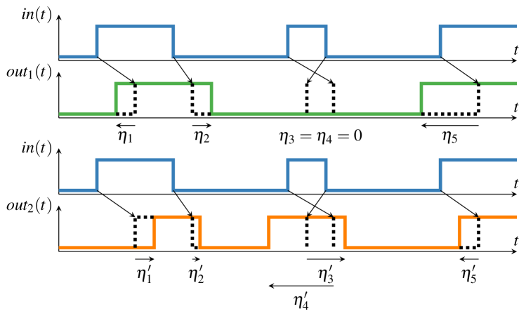
for a falling transition, where and are the time of the current resp. previous input transition, and . Fig. 2 illustrates two of the infinitely many possible output signals of a channel in the -IDM, for a fixed input signal, where the dashed lines represent the deterministic delay prediction by the IDM. It is apparent that the adversary has the power to cancel or uncancel pulses w.r.t. the deterministic prediction.
Since faithfulness is defined with respect to the Short-Pulse Filtration (SPF) problem, we recall its definition here. Informally, it is similar to the problem of building an inertial delay channel from a single input up-down pulse of length starting at time :
Definition 1 (Short-Pulse Filtration, see [7]).
A circuit that solves SPF needs to adhere to the following constraints:
-
F1)
Well-formedness: The circuit has exactly one input and one output port.
-
F2)
No generation: The circuit does not generate a pulse on the output, if no pulse is on the input.
-
F3)
Nontriviality: The output is not the zero signal for all pulses.
-
F4)
No short pulses: There exists an such that the output signal does not contain pulses of length less than .
For the bounded version of SPF, there is an additional constraint:
-
F5)
Bounded stabilization time: There exists a such that for every input pulse the last output transition is before time .
For any input signal other than a single pulse, we allow the SPF circuit to behave arbitrarily.
In order to show that the -IDM does not allow to solve bounded SPF, the authors of [11] used a simple reduction proof: By setting all delay variations , the model degenerates to the plain IDM, where this is known to be impossible [7]. The other case, namely, showing that it is possible to solve unbounded SPF in the -IDM, turned out to be trickier: For the SPF circuit given in Fig. 3, they analyzed all possible behaviors via a case distinction on the length of the input pulse (short, large and medium). The most delicate case turned out to be medium pulse lengths, where a critical (infinite) pulse train with up-time and down-time may be generated. It occurs if the adversary maximally delays all rising transitions (by ) and minimally delays all falling transitions (by ), provided the (quite restrictive) constraint
| (C1) |
holds. If the adversary chooses delay variations that ever cause the up-time of a pulse to become larger than , it cannot revert to pulses with shorter up-times again, and hence cannot prohibit the feedback loop of the OR gate to eventually lock at 1. Consequently, a correct SPF circuit is obtained by letting the high-threshold buffer at the output map all pulse trains with up-times less or equal to constant , as all pulse trains that ever exceed will lead to a single rising transition at the output.

III Extending the Variation Range of the -IDM
In this section, we will show that the range of adversarial variations of the -IDM can be increased substantially, without sacrificing faithfulness with respect to the SPF problem. The crucial idea of our extension is to introduce -dependent bounds in the variation range , which coincide with the original bounds only for two very small values of , which are quite insensitive to delay fluctuations.
Let be the up-time of the critical pulse train identified in [11] (which is determined by the fixed point of given in Eq. 7) and be the unique minimum delay value of a strictly causal111Where and . IDM channel, defined by
| (3) |
according to [7, Lem. 3].
Definition 2.
For some given constants
| (C2) |
some , , some satisfying , and , let
| (4) |
| (5) |
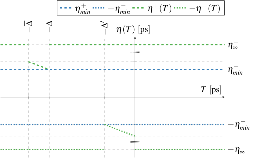
Fig. 4 shows the comparison of the old and the new bounds for the -IDM. Note carefully that the only values of for which the bounds could not be enlarged are and , i.e., the up-time and the down-time of the critical infinite pulse train identified in [11]. For the inverter used in Section V, the actual values are and . Both and are hence approximately times larger than the original bounds and here.
For proving the faithfulness of the extended -IDM, we show:
-
G1)
There is no circuit with extended -IDM-channels that can solve bounded SPF.
-
G2)
There exists a circuit with extended -IDM-channels that can solve unbounded SPF.
For G1), the exact same proof as in the original -IDM paper [11] can be used: Setting all the adversarial delays lets the -IDM-channel degenerate to an IDM-channel, which does not allow solve bounded SPF [7].
The intricate part is again the proof of G2), where we split the range of the input pulse lengths into three intervals.
Lemma 3.
If the input pulse length satisfies for , then the output of the OR gate in Fig. 3 has a rising transition at time and no falling transitions.
Proof.
The rising transition from the input arrives at latest at at (one can assume that the OR gate has been initialized to output 0 at time ). Therefore, the falling transition on input happens at or after , so has no influence on the output of the OR gate: the feedback loop hence locks at constant . ∎
Lemma 4.
If the input pulse length satisfies , then the output pulse of the OR gate in Fig. 3 only contains the input pulse.
Proof.
The earliest time that the rising transition from can be propagated to is now . Therefore, for the falling transition, we get , the falling output transition on hence cannot occur later than . The two transitions on cancel each other out iff , i.e., iff
| (6) |
Note that the upper bound on given in Lemma 4 already implies the constraint
| (C3) |
The most delicate part of the proof are again medium-sized input pulses, i.e., where . Inspired by [11], we also consider a self-repeating critical pulse train, by letting the adversary choose all rising transitions maximally late () and all falling transitions maximally early (). Formally, for a pulse of length , the length of the next pulse can be calculated as:
| (7) |
where and are given by Definition 2. The period resp. involving the pulse , measured from the rising transition of to the rising transition of resp. the falling transition of to the falling transition of , is
| (8) |
We note that the length of the next pulse and the periods of the critical pulse train established in [11] are
| (9) | ||||
which were shown in [12, Lem. 5] to have a fixed point and a period for some , provided the constraint Eq. C1 holds.
Lemma 5.
Proof.
Plugging in in Eq. 7 and applying the definition for and from Definition 2 yields
| (10) |
In order to guarantee diverging from the critical pulse train for excessive pulses, we need a bound on the derivative of :
Lemma 6.
For defined in Eq. 7, we have for , provided
| (C4) |
Proof.
Calculating the derivative of yields:
| (11) | ||||
| (12) |
To justify Eq. 11, we note that and are strictly increasing and concave, so and . Moreover, is decreasing in , hence can be lower bounded by since , and and according to Definition 2. Choosing and according to the sufficient condition Eq. C4 finally ensures . ∎
As the next step in our proof, we need to show that pulses that are larger than cannot come back, i.e., if ever holds, then for every :
Lemma 7.
It holds that if , provided that and are chosen according to Eq. C4.
Proof.
From the mean value theorem of calculus, we know that
| (13) |
Applying the fact that and rearranging yields . From Lemma 6, we know that , and hence , if and are chosen appropriately. ∎
It still remains to be shown that the feedback loop locks at 1 when the pulse width reaches given in Definition 2:
Lemma 8.
The feedback loop locks when the pulse length satisfies .
Proof.
The feedback loops locks at 1 if the rising transition of pulse is scheduled before or at the same time as the falling transition of pulse . This cancellation happens when , which is implied by the assumption on stated in our lemma and the definition of for given in Definition 2. ∎
Theorem 9.
The new bounds ensure that pulses which are larger than are monotonically increasing until the pulse length reaches and the feedback loop locks at 1.
Theorem 10.
Consider the circuit in Fig. 3 subject to the following constraints:
-
(C1)
-
(C2)
,
-
(C3)
-
(C4)
.
The OR gate fed-back by a strictly causal -IDM channel has the following output when the input pulse has length :
-
(i)
If the input pulse length is , then the output of the OR gate has a unique rising transition at time and no falling transitions.
-
(ii)
If the input pulse length is , then the output pulse of the OR gate only contains the input pulse.
-
(iii)
If , then the output may resolve to a constant or , or may be an (infinite) pulse train with a maximum pulse up-time of and a maximum duty cycle of .
Proof.
By combining Lemmas 3, 4, 5 and 9, the resolution to 1 resp. the maximum up-time bound follow immediately. To also confirm the upper bound on the duty cycle, we show by contradiction that no infinite pulse train can contain a pulse with a down-time : Since by Eq. 8, it decreases with both and . Hence, if ever occurred, we would get . Hence, it follows that , which contradicts the upper bound established before. ∎
It only remains to properly choose the high-threshold buffer at the output of the OR gate. First, it must map infinite and decreasing pulse trains ( for ) according to (iii) in Theorem 10 to the zero signal. Second, for an increasing pulse train (some ), it needs to be ensured that once the high-threshold buffer switches to one it never switches back. It has been shown in [11, Lem. 3] that it is possible to implement a high-threshold buffer with the required properties with a simple exponential IDM channel (an exp-channel, see [9] for details), which finally establishes:
Theorem 11.
There is a circuit that solves unbounded SPF in the extended -IDM.
IV The -CIDM
In this section, we will sketch how the extended -IDM and the Composable Involution Delay Model (CIDM) [10] can be seamlessly combined. The CIDM generalizes the IDM by adding a transition-dependent pure-delay shifter (with resp. affecting resp. only) at each input of a gate, and re-ordering/changing the different internal components of IDM channels, as shown in Fig. 5 for the SPF circuit in Fig. 3. The pure-delay shifter can be used to account for threshold voltage variations between gates, which considerably decreases the circuit characterization effort: a single threshold voltage like can be used for all gates of a circuit. Moreover, the pure-delay shifter makes it easy to implement high-threshold buffers with arbitrary threshold voltages.

CIDM channels are characterized by the delay functions
| (14) | ||||
| (15) |
which do not satisfy the involution property. Still, it turned out that the result of concatenating the tail (the IDM channel ) of the CIDM of a predecessor gate with the head (the pure delay shifter and the cancellation unit ) of the CIDM of the successor gate does form a regular IDM channel (albeit with delay functions that are usually different from and ). Consequently, it is possible to transfer results obtained for circuits made up of IDM channels to circuits made up of CIDM channels. In particular, this is true for our extended -IDM, as the SPF circuit shown in Fig. 5 is indeed equivalent (modulo some pure delay shifts) to Fig. 3.
In the -CIDM, a CIDM-channel with an appropriately chosen and can be used to replace the exp-channel-implementation of the high-threshold buffer used in [11]:
Lemma 12.
For any , the high-threshold buffer in Fig. 5 can be implemented by a strictly causal CIDM-channel, which ensures that all pulses (at ) with up-time are canceled and the zero signal is generated at and hence .
Proof.
The adversaries in the feedback loop () and between the OR gate and the high-threshold buffer () can add variations in the range [] resp. []. Note that we can neglect the -dependency for the adversaries here and just use the maximum possible delay variation. By back-tracking the pulse through , and the adversary , the maximum length of the corresponding up-pulse at can be determined as:
| (16) |
It is achieved if the rising transition is maximally delayed and the falling transition is minimally delayed by the adversary. Consequently, we obtain for . It thus suffices to choose and such that all up-pulses are mapped to constant , which is ensured if
| (17) |
holds. Since it has been shown in [10] that can be chosen arbitrarily large (whereas is lower-bounded in order not to violate strict causality of the CIDM channel), Eq. 17 can always be satisfied. Note that, unlike for the high-threshold buffer implementation with the exp-channels used in [11], it is easy to determine the necessary parameters via Eq. 17 here. Moreover, the upper bound on the duty cycle established in Theorem 10 is not needed anymore.
However, we still need to argue that the additional IDM-channel and the adversary at the output of the high-threshold buffer do not have adverse effects. Fortunately, for the output , we only need to distinguish two possible cases: (i) If there is no transition at , then there is obviously also no transition at . (ii) If there is a single rising transition at the output at time , then this single transition is propagated to at some time . The output is hence still in accordance with the behavior of a high-threshold buffer. ∎
We hence obtain our desired result:
Theorem 13.
There is a circuit that solves unbounded SPF in the -CIDM.
Proof.
If , then the output only contains the input pulse , according to Theorem 10. By Lemma 12, we know that we can choose such that this pulse is mapped to a constant .
If , then the output has a single rising transition at . Eventually, the output of the high-threshold buffer also has a single transition to .
If is in between the above ranges, two cases can be distinguished: (i) Suppose that the up-pulse lengths never exceed , then Lemma 12 for any guarantees that the input is mapped to a constant at the output of the high-threshold buffer. For the other case (ii), the pulse length of the pulse train (eventually) exceeds . By Theorem 9 it is guaranteed that the feedback loop will eventually lock at constant . If we choose such that all pulses with a width at most are mapped to a constant , we can ensure that the high-threshold buffer has exactly one rising transition after the feedback loop has locked. ∎
V Simulation results
In this section, we will show222Due to space constraints, we can only provide a few of our experimental results. that the delay predictions of our new -CIDM cover the actual delays of an inverter chain under substantial PVT variations and even under aging.
For our evaluation, we used Cadence Spectre (version 20.1) [13] to simulate a 7-stage inverter chain in UMC technology (G-05-LOGIC/MIXED_MODE28N-HPC-SPICE). Since their model cards not only offer parameter sets for different process corners, i.e., different combinations of fast and slow n-MOS resp. p-MOS transistors, but also parameters for simulating Negative Bias Temperature Instability (NBTI), Positive Bias Temperature Instability (PBTI) and Hot Carrier Injection (HCI), we could use the RelXpert tool [14] to compute aged versions of the circuit (with transistors suffering from threshold voltage shifts and gate oxide damages). Since we did not have a gate library for the used technology, however, we had to design our own inverter cells. We choose and , which are within the specified range according to the data sheet and between the values for comparable and technologies.
To compare the delays of the actual circuit and the predictions of our model, we had to perform the following steps:
-
(1)
Obtain the delay functions and via analog simulations under the default environment (, ).
-
(2)
Extract the parameters for our delay model, based on and .
-
(3)
Run analog simulations under PVT variations and aging, and obtain the appropriate delay functions and , where
-
(4)
Compare the old and the new “corridor” of the -CIDM, i.e., its deterministic delay prediction + the allowed variation range, with the actually measured delay functions.
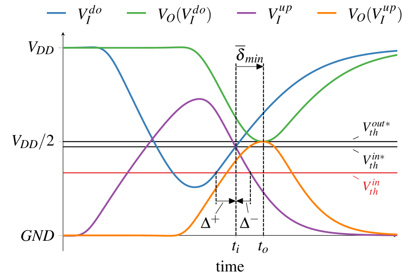
To characterize our circuit in steps (1) and (2), i.e., to determine the parameters and and the actual delay function and of every gate, we used333The publicly available Involution Tool [9] provides characterization scripts, which we extended appropriately to perform the procedure described below fully automatically. the approach from [10]. It is illustrated in Fig. 6: First, running analog simulations for each pulse width, a binary search on the input pulse width is used until the output trajectory for the falling (green) and rising (orange) transition both touch . Then, the rising input and the corresponding output trajectory is moved in time until the rising and falling output trajectories touch each other at . Now, is just the time between the touching point of the output trajectories and the crossing point of the input trajectories. resp. is determined as the time for the rising resp. falling input trajectory to get from to .
In order to determine and , we first measured the actual delays, by sending longer pulses through the circuit and recording the pair for each input/output trajectory. Then, the parameters of a SumExp-IDM channel [9] were fitted to these empirical delay functions using a least squares approach. For the adversary, we choose symmetric parameters, i.e., and .
For step (3), we had to repeat the characterization of the circuit for the PVT variations and aging considered.
In step (4), all simulated delay functions were compared to the corridor of the delay predictions of the -CIDM: Fig. 7 shows the results for the rising delay function between the fourth and fifth inverter of the circuit. The delay function (blue) is the baseline, obtained via analog simulations. The deterministic delay function of the -CIDM (red) has been least squares fitted to . The old (narrow) corridor is shown in green, whereas the significantly larger new corridor is lilac.
It is immediately apparent that it was already difficult to fit a channel to the baseline (without PVT variations and aging) when using the old bounds (compare [11, Fig. 9]), whereas this is absolutely no problem for our bounds.
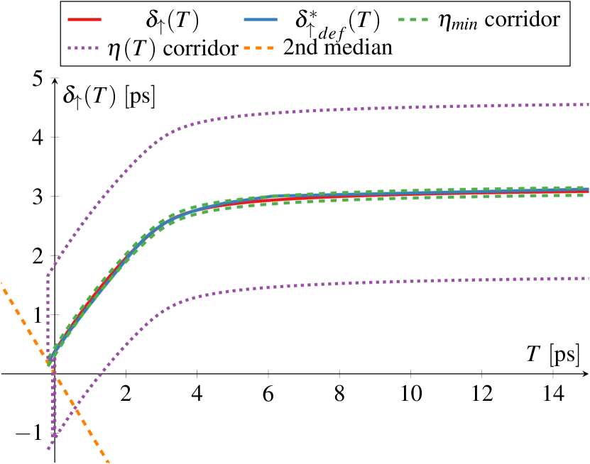
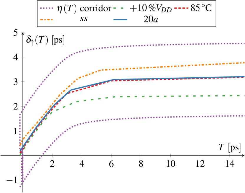
Fig. 8 shows the PVT variations and aging results for the rising delay function between the fourth and fifth inverter. Note that the results for the other gates in the circuit are comparable. The delay function with 10 % increased supply voltage is obviously faster than the one under the default environment. For an increased temperature of , the resulting delay function is only slightly slower. The same also holds for the circuit that is aged by 20 years. Fig. 8 also shows the slow down for the process corner ss, i.e. a slow n-MOS and a slow p-MOS transistor. It is apparent that all these PVT variations and aging are covered by our new model.
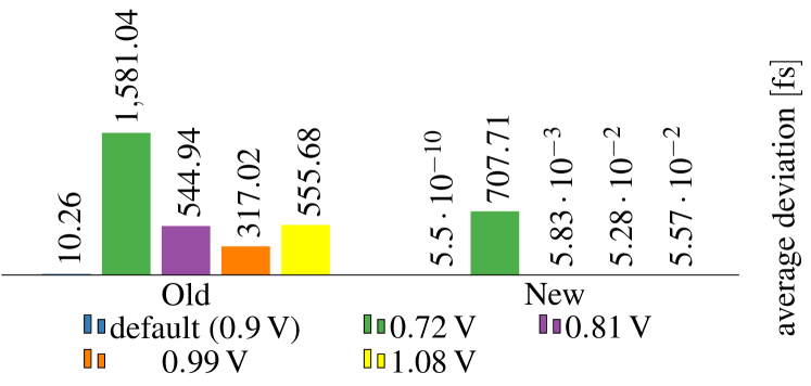
To complement the above results, we also evaluated the average coverage of the -CIDM for the entire circuit. More specifically, we considered both and for all seven inverters and numerically integrated over the difference between the measured delays and the respective corridor, for every recorded value of . If the delay function is inside the corridor, the contribution to the integral is , otherwise it is the distance to the closest corridor border. By normalizing the resulting value to the integration interval, we obtain a value that can be viewed as the average coverage violation, i.e., the average time deviation from the corridor.
Fig. 9 shows the results for supply voltage variations. It can be seen that the average deviation is significantly larger for the old bounds, whereas there is almost no deviation for the new bounds. A significant deviation is observed only for , which is unlikely to happen in modern VLSI circuits.
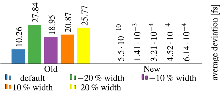
Like in the -IDM-paper [11], we also considered transistor width variations. Again, Fig. 10 reveals that our new bounds perfectly cover even substantial variations, unlike the old bounds, which result in significant deviations (albeit not as large as for variations).
Overall, our results confirm that the -CIDM indeed surpasses the coverage of the original -IDM of [11] substantially.
VI Conclusion
We provided a new unbounded single-history delay model, the -CIDM, which supports a large range of adversarial delay variations. It substantially improves on the existing -IDM, by making the delay variation range dependent on every transitions’ particular input-to-previous-output time. We proved analytically that this extension does not invalidate the implementability of SPF, hence preserves faithfulness. By means of exhaustive simulations, we showed that our -CIDM, unlike the original -IDM, can cover a substantial range of PVT variations and aging.
References
- [1] M. Bouvier, A. Valentian, T. Mesquida, F. Rummens, M. Reyboz, E. Vianello, and E. Beigne, “Spiking neural networks hardware implementations and challenges: A survey,” J. Emerg. Technol. Comput. Syst., vol. 15, no. 2, apr 2019. [Online]. Available: https://doi.org/10.1145/3304103
- [2] Synopsis Inc., CCS Timing Library Characterization Guidelines, Synopsis Inc., October 2016, version 3.4.
- [3] Cadence Design Systems, Effective Current Source Model (ECSM) Timing and Power Specification, Jan. 2015, version 2.1.2.
- [4] S. H. Unger, “Asynchronous sequential switching circuits with unrestricted input changes,” IEEE ToC, vol. 20, no. 12, pp. 1437–1444, 1971.
- [5] M. J. Bellido-Díaz, J. Juan-Chico, and M. Valencia, Logic-Timing Simulation and the Degradation Delay Model. London: Imperial College Press, 2006.
- [6] M. Függer, R. Najvirt, T. Nowak, and U. Schmid, “Towards binary circuit models that faithfully capture physical solvability,” in Proc. DATE’15, March 2015, pp. 1455–1460.
- [7] M. Függer, R. Najvirt, T. Nowak, and U. Schmid, “A faithful binary circuit model,” IEEE TCAD, vol. 39, no. 10, pp. 2784–2797, 2020.
- [8] M. Függer, T. Nowak, and U. Schmid, “Unfaithful glitch propagation in existing binary circuit models,” IEEE ToC, vol. 65, no. 3, pp. 964–978, 2016.
- [9] D. Öhlinger, J. Maier, M. Függer, and U. Schmid, “The involution tool for accurate digital timing and power analysis,” Integration, vol. 76, pp. 87 – 98, 2021.
- [10] J. Maier, D. Öhlinger, U. Schmid, M. Függer, and T. Nowak, “A composable glitch-aware delay model,” in Proc. GLSVLSI’21, 2021, pp. 147–154. [Online]. Available: https://doi.org/10.1145/3453688.3461519
- [11] M. Függer, J. Maier, R. Najvirt, T. Nowak, and U. Schmid, “A faithful binary circuit model with adversarial noise,” in Proc. DATE’18, March 2018, pp. 1327–1332. [Online]. Available: https://ieeexplore.ieee.org/document/8342219/
- [12] ——, “A faithful binary circuit model with adversarial noise,” 2020. [Online]. Available: https://arxiv.org/abs/2006.08485
- [13] Cadence Design Systems, Spectre® Circuit Simulator Reference, product version 20.1 ed., Cadence Design Systems, Sep. 2020.
- [14] ——, Spectre® RelXpert Reliability Simulator User Guide, product version 20.1 ed., Cadence Design Systems, Sep. 2020.