Structure Prediction of Epitaxial Organic Interfaces with Ogre, Demonstrated for TCNQ on TTF
Abstract
Highly ordered epitaxial interfaces between organic semiconductors are considered as a promising avenue for enhancing the performance of organic electronic devices including solar cells, light emitting diodes, and transistors, thanks to their well-controlled, uniform electronic properties and high carrier mobilities. Although the phenomenon of organic epitaxy has been known for decades, computational methods for structure prediction of epitaxial organic interfaces have lagged far behind the existing methods for their inorganic counterparts. We present a method for structure prediction of epitaxial organic interfaces based on lattice matching followed by surface matching, implemented in the open-source Python package, Ogre. The lattice matching step produces domain-matched interfaces, where commensurability is achieved with different integer multiples of the substrate and film unit cells. In the surface matching step, Bayesian optimization (BO) is used to find the interfacial distance and registry between the substrate and film. The BO objective function is based on dispersion corrected deep neural network interatomic potentials, shown to be in excellent agreement with density functional theory (DFT). The application of Ogre is demonstrated for an epitaxial interface of 7,7,8,8-tetracyanoquinodimethane (TCNQ) on tetrathiafulvalene (TTF), whose electronic structure has been probed by ultraviolet photoemission spectroscopy (UPS), but whose structure had been hitherto unknown [Organic Electronics 48, 371 (2017)]. We find that TCNQ(001) on top of TTF(100) is the most stable interface configuration, closely followed by TCNQ(010) on top of TTF(100). The density of states, calculated using DFT, is in excellent agreement with UPS, including the presence of an interface charge transfer state.
I Introduction
Organic-organic heterojunctions, i.e., interfaces between different organic materials, are at the heart of organic electronic devices, including organic photovoltaics (OPV),Mazzio and Luscombe (2014); Kippelen and Brédas (2009) organic light emitting diodes (OLEDs),Reineke et al. (2013); Liu et al. (2018); Brütting, Berleb, and Mückl (2001); Armstrong et al. (2009) and organic field effect transistors (OFETs).Mas-Torrent and Rovira (2011); Chen et al. (2020); Sirringhaus (2014); Braga and Horowitz (2009); Wang et al. (2022) Essential device functionalities take place at interfaces. In organic solar cells, charge separation of bound excitons into free charge carriers occurs at donor-acceptor interfaces, where the holes go into the highest unoccupied molecular orbital (HOMO) of the donor and the electrons go into the lowest unoccupied molecular orbital (LUMO) of the acceptor. Conversely, in OLEDs, electrons and holes recombine at a donor-acceptor interface, leading to photon emission.Armstrong et al. (2009) In more sophisticated multilayer OLED designs, additional functions may be separated into different materials. A multilayer OLED may include a hole-injection layer, a hole-transport layer, an electron-blocking layer, an emission layer, a hole-blocking layer, an electron-transport layer, and an electron-injection layer, forming multiple active interfaces.Reineke et al. (2013) In OFETs, the gate stack contains, at the minimum, an organic semiconductor interfaced with the gate dielectric and the source and drain electrodes. In some cases, more than one organic semiconductor is included in the gate stack to create an -channel and a -channel. Additional organic layers may be included, e.g., to control the morphology of the organic semiconductor(s) and the contact resistance at the electrode interfaces.Chen et al. (2020) Hence, the structure and electronic properties of organic interfaces are critical to the performance of organic electronic devices.
Often, the films used in organic devices are amorphous and the interfaces between them are disordered. Disorder may lead to non-uniform electronic and optical properties that are averaged over multiple configurations.Khan and Rand (2021); Khan et al. (2019) In addition, various defects, as well as grain boundaries in polycrystalline films,Choi et al. (2020) may form traps and provide scattering sites for charge carriers. This is detrimental to charge transport and lowers the carrier mobility, which is a key performance parameter for electronic devices. Molecular order produces well-controlled properties and higher mobilities, which may lead to improved device performance.Gershenson, Podzorov, and Morpurgo (2006); Coropceanu et al. (2007); Nakayama, Kera, and Ueno (2020); Podzorov (2013); Li et al. (2010); Reese and Bao (2007); Fusella et al. (2018); Raimondo et al. (2011); Wang et al. (2022) In analogy with inorganic materials, high-quality crystalline organic heterojunctions may be grown by molecular beam epitaxy. Schreiber (2004); Forrest et al. (1994); Moret et al. (2011); Sassella (2013); Koma (1995, 1999); Fenter et al. (1997); Forrest and Zhang (1994); Hooks, Fritz, and Ward (2001); Yang and Yan (2009); Yang, Yan, and Jones (2015) In contrast to inorganic epitaxy, molecular materials are bound by weak dispersion interactions and organic substrates do not have dangling bonds on the surface. Moreover, there is competition between adsorbate-substrate and adsorbate-adsorbate intermolecular interactions. This leads to less strict lattice-matching requirements between the substrate and film for organic epitaxial growth.Koma (1995); Forrest (1997); Yang and Yan (2009); Yang, Yan, and Jones (2015) Epitaxial interfaces between various organic semiconductors have been grown, including -quaterthiophene on rubreneCampione et al. (2009), pentacene on Al-Mahboob et al. (2009), rubrene on tetraceneMoret et al. (2011), on pentaceneNakayama et al. (2016, 2018); Conrad et al. (2009); Huttner, Breuer, and Witte (2019); Iwasawa et al. (2020) or rubreneFusella et al. (2018); Mitsuta et al. (2017), perfluoropentacene on pentaceneNakayama et al. (2019) or diindenoperylene (DIP) Hinderhofer et al. (2011), DIP on copper-hexadecafluorophthalocyanine (F16CuPc) Barrena et al. (2006), bis(trifluoromethyl)dimethylrubrene on rubrene Takahashi et al. (2021), tetraazanaphthacene on pentacene,Gunjo et al. (2021) and 7,7,8,8-tetracyanoquinodimethane (TCNQ) on tetrathiafulvalene (TTF) Kattel et al. (2017). Band transport has been observed in organic epitaxial interfaces.Nakayama et al. (2019); Fusella et al. (2018) Moreover, epitaxial interfaces with a well-defined structure and uniform properties are conducive to spectroscopic characterization of the interface band alignment, interface charge transfer (CT) states, and exciton dynamics.Iwasawa et al. (2020); Takahashi et al. (2021); Kattel et al. (2017); Conrad et al. (2009); Gunjo et al. (2021); Döring et al. (2019)
Computer simulations can help explore the vast configuration space of possible substrate and film combinations to direct fabrication efforts to systems likely to result in robust epitaxial growth of high-quality films. Furthermore, simulations can help the characterization of epitaxial organic interfaces by assigning spectroscopic signatures to putative interface structures. The structure prediction capabilities for organic interfaces lag far behind the existing methods for inorganic interfaces. Several computational tools and codes exist for constructing models of inorganic epitaxial interfaces.Dardzinski et al. (2022); Moayedpour et al. (2021); Mathew et al. (2016); Ding et al. (2016); Raclariu et al. (2015); Sun and Ceder (2013); Gao et al. (2019) Because these tools are designed to work with spherical atoms, not molecules, which are significantly more complex, they do not work out of the box for organic interfaces. Recently, progress has been achieved in the development of algorithms for structure prediction of organic monolayers on inorganic substrates.Mannsfeld and Fritz (2011); Packwood and Hitosugi (2017); Packwood, Han, and Hitosugi (2017); Obersteiner et al. (2017); Scherbela et al. (2018). Organic-organic interfaces have been investigated mainly by molecular dynamics simulations, based on classical force fields, which enable studying the effect of disorder.Han, Shen, and Yi (2015); Fu et al. (2014); Fu, Risko, and Brédas (2013); Yoo et al. (2019) However, to our knowledge, to date, no computational tools have been developed for structure prediction of epitaxial organic-organic interfaces.
Here, we introduce a new version of the open source Python package, Ogre, with new functionality of predicting the structure of epitaxial organic interfaces by lattice and surface matching. We note that Ogre generates ideal interfaces with no disorder and does not take into account growth conditions and kinetics. The first version of Ogre was designed for modelling molecular crystal surfaces, calculating surface energies, and predicting Wulff shapes.Yang et al. (2020) In the second version, the capability of performing structure prediction for epitaxial inorganic interfaces was added.Moayedpour et al. (2021) Similar to the previous version of Ogre, the workflow for organic interfaces begins by using Zur and McGill’s lattice matching algorithmZur and McGill (1998) and proceeds to perform surface matching. The lattice matching step identifies potential domain-matched epitaxial interfaces, where commensurability is achieved with different integer numbers of the substrate and film unit cells. The lattice misfit tolerances for domain matching have been updated for the case of weak van der Waals epitaxy. In addition, a streamlined calculation of the surface energies of different substrate facets may be performed to prioritize the most stable orientations for an interface Miller index search. In the surface matching step, Bayesian optimization (BO) is utilized to find the most stable interface configurations by exploring the three-dimensional space of interfacial distance and registry.
For surface matching, Ogre constructs commensurate surface unit cells of the substrate and film, ensuring that no molecules are broken when the surface is cleaved.Yang et al. (2020) The film is then moved with respect to the substrate in order to determine the optimal configuration. Owing to the large domain size and the number of atoms per molecule, even the smallest models of organic epitaxial interfaces, with only one layer of the substrate and the film, may contain hundreds to thousands of atoms. Therefore, it is imperative to use a computationally efficient method for evaluating the relative stability of interface configurations. The geometric score function we developed for inorganic interfacesMoayedpour et al. (2021) is not appropriate for organic interfaces because it is designed to work with spherical atoms, whose radii are determined by Hirshfeld partitioningSpackman and Jayatilaka (2009) of the charge density of the bulk materials calculated with density functional theory (DFT). Instead, we use the Accurate Neural Network Engine for Molecular Energies (ANI) general-purpose machine learned interatomic potentials.Smith, Isayev, and Roitberg (2017) The ANI deep neural network potentials have been trained on a large and diverse database of first principles calculations for small molecule conformationsSmith et al. (2020) using active learningSmith et al. (2018). They have been shown to be transferable across chemical space, achieving a DFT level of accuracy on a large set of organic molecules while being six orders of magnitude faster. Because the ANI potentials were trained on isolated molecules they do not inherently contain a description of intermolecular dispersion (van der Waals) interactions. Therefore, the Grimme D3 dispersion correction is added to the ANI energies.Smith et al. (2016); Grimme, Ehrlich, and Goerigk (2011); Ehrlich et al. (2011) We show that ANI+D3 is in close agreement with DFT for the interfacial distance and registry. Preliminary ranking of the interface energies of the surface-matched configurations of all domain-matched interfaces is performed with ANI+D3. The ANI+D3 ranking is in reasonably good agreement with the DFT ranking and the most stable structures are identified. In the final stage, DFT is used to calculate the electronic properties of a small subset of the most promising candidate structures.
The application of Ogre is demonstrated for the epitaxial interface of TCNQ grown on top of TTF.Kattel et al. (2017) TTF and TCNQ are a quintessential donor/acceptor system. Both TTF and TCNQ are wide band gap semiconductors. On their own, they are insulators but when they are paired, electrons can transfer from the HOMO of TTF to the LUMO of TCNQ.Kattel et al. (2017); Murdey and Salaneck (2005); Braun et al. (2010); Beltrán et al. (2013); Atalla et al. (2016) Hence, TTF-TCNQ co-crystals and interfaces may exhibit metallic behavior. The conducting layer, which forms at the interface, has been reported to exhibit a high carrier density, exceeding .Kattel et al. (2017); Ando et al. (2008); Cohen et al. (1974); Ferraris et al. (2002) The interface formed by TTF and TCNQ single crystals has been found to exhibit 2D metallic conductivity, which may be useful for organic transistors and sensing devices.Alves, Pinto, and MaçÔas (2013); Krupskaya et al. (2016); Krupskaya, Lezama, and Morpurgo (2016); Takahashi et al. (2012); Mathis et al. (2012); Lezama et al. (2012); Calhoun et al. (2007); Alves et al. (2008) Kattel et al. have grown an epitaxial interface of TCNQ on top of TTF.Kattel et al. (2017) The electronic structure of the interface was probed by ultraviolet photoemission spectroscopy (UPS) as a function of the thickness of the TCNQ film. A charge transfer (CT) state was observed at the interface, whose signature decayed when the TCNQ film thickness exceeded 2 nm. However, the interface was not structurally characterized, leaving the orientation of the TTF and TCNQ and their relative positions at the interface hitherto unknown. Using Ogre, we find that TCNQ(001) on top of TTF(100) is the most stable interface configuration, closely followed by TCNQ(010) on top of TTF(100). The resulting density of states (DOS) of the TTF substrate, a TCNQ film, and an interface with one layer of each material are in excellent agreement with the UPS experiment of Kattel et al.. A CT state is found at the interface, consistent with their observations.
II Computational Details
II.1 DFT
The all-electron electronic structure code FHI-aimsBlum et al. (2009) was used to perform DFT calculations. Computationally efficient light numerical settings and tier 1 basis sets were used throughout, owing to the large system sizes with several hundred atoms. Geometry optimizations, surface energy evaluations, reference DFT calculations for surface matching, and interface energy evaluations were conducted using the generalized gradient approximation of Perdew, Burke, and Ernzerhof (PBE)Perdew, Burke, and Ernzerhof (1996, 1997) with the Tkatchenko-Scheffler (TS) pairwise dispersion method. Tkatchenko and Scheffler (2009) Structural relaxations were performed for the bulk crystal structures of TTF and TCNQ until the residual force per atom was less than ev/Å. Relaxation was performed with fixed unit cell angles of = for TTFBatsanov (2006) and = for TCNQ.Krupskaya et al. (2015) The number of k-points in each direction was determined by calculating the closest integer greater than 24 divided by the norm of the respective lattice parameter. The relaxed lattice parameters of TTF were = 7.44 Å, = 4.28 Å, and = 13.68 Å, compared with the experimental values of = 7.35 Å, = 4.01 Å, and = 13.901 Å.Batsanov (2006) The relaxed lattice parameters of TCNQ were = 8.98 Å, = 7.31 Å, and = 16.40 Å, compared with the experimental values of = 8.8834 Å, = 6.9539 Å, and = 16.3948 Å.Krupskaya et al. (2015) The interface models were constructed based on the relaxed bulk geometry with one layer of the TTF substrate, one layer of the TCNQ film, and a vacuum region of 40 Å. The electronic structure calculations for the the final lowest energy interfaces were performed using the range-separated hybrid functional of Heyd–Scuseria–Ernzerhof (HSE).Heyd, Scuseria, and Ernzerhof (2003, 2006) We note that the size of the systems calculated here is very large. For example, the TCNQ(001)/TTF(100) interface model with a single layer of each material contained 1298 atoms.
II.2 ANI neural network potentials
The ANAKIN-ME (ANI)Smith, Isayev, and Roitberg (2017) transferable neural network molecular potentials are used for calculations of organic interfaces. The representation used by the ANI-2x modelDevereux et al. (2020) is the Smith symmetry functions (SSFs), , a modified version of the Behler and Parrinello symmetry functions. A separate neural network model is used for each element. The SSFs encode N inter-atomic distances between the atom and its neighbors within a cutoff radius into an invariant fixed-length atomic environment vector (AEV), . The elements encodes specific regions of an individual atom’s radial and angular chemical environment. Each for the atom with atomic number is then used as input into a single neural network (NNP). With an invariant AEV, , the total energy of a molecule is expressed as:
| (1) |
The ANI-2x potentials have been trained on a large and diverse dataset of first-principles calculations for small organic molecules selected by an active learning procedure.Smith et al. (2018) Test cases have demonstrated the ANI potentials to be chemically accurate compared to reference DFT calculations. The Grimme D3 dispersion correctionGrimme et al. (2010) is added post hoc to ANI-2x calculations to account for intermolecular van der Waals interactions. All functionality is implemented in the open source TorchANIGao et al. (2020) package (https://github.com/aiqm/torchani), which is written in python using the PyTorch library. TorchANI is designed to take advantage of the modularity and simplicity of PyTorch to provide a framework for fast iterative improvements in architecture and training schedules for ML models, while also allowing for experimentation and easy integration into existing software, such as Ogre.
III Results and Discussion
III.1 Workflow Overview
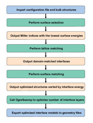
Ogre is written in Python 3. It employs several modules from the Python Materials Genomics (pymatgen) Ong et al. (2013) and the Atomic Simulation Environment (ASE) Larsen et al. (2017) libraries. The package can be downloaded from www.noamarom.com under the terms of a BSD-3 license. The inputs of Ogre are the bulk structures of the substrate and film materials, as well as a configuration file with user-specified settings for directing the workflow of Ogre. Standard input structure file formats such as the POSCAR format of the Vienna ab initio Simulations Package’s (VASP) Joubert (1999); Kresse and Furthmüller (1996); Kresse1CI9C6a; Kresse and Hafner (1993, 1994), crystallographic information files (CIF), and the geometry.in format of the FHI-aims code Blum et al. (2009) are supported by Ogre. Figure 4 shows an overview of the workflow of interface structure prediction with Ogre. Ogre’s workflow includes four main steps: surface selection (Section III.2), lattice matching (Section III.3), surface matching (Section III.4), and ranking (Section III.5). Finally, the electronic properties may be calculated for the interface(s) predicted to be the most stable (Section III.6)
As a preliminary step, Ogre may be used for substrate and surface selection. For organic epitaxy, substrates that form platelets are desirable.Dull et al. (2020) Ogre’s morphology prediction capability Yang et al. (2020) could be used for substrate screening. If the substrate has already been chosen, as in the case of the TCNQ/TTF interface studied here, but the orientation is unknown, Ogre may be used to calculate the surface energy of all the symmetrically unique facets up to a selected Miller index.Yang et al. (2020) The lowest energy surfaces form the largest facets and are best suited to serve as the substrate for epitaxial growth. Lattice matching may then be performed for the chosen facets.
The lattice matching step for organic interfaces is similar to inorganic interfaces.Moayedpour et al. (2021) Ogre uses the algorithm of Zur and McGillZur and McGill (1984) to identify all domain-matched supercells of the substrate and film within the user-defined tolerances for interface area and lattice misfit. A Miller index scan can be performed if the substrate and/or film have multiple possible orientations. The maximum interface area, the misfit tolerance, and the Miller indices for the substrate and film are the input parameters for lattice matching. The lattice matching step generates a list of structures that are sorted by super-cell area misfit values. As explained above, owing to the weak nature of dispersion interactions in organic materials, robust epitaxial growth can occur at higher interface misfit values compared to inorganic interfaces.Sassella, Campione, and Borghesi (2008); Sassella (2013) Therefore, a looser default tolerance of 5% has been adopted for the supercell area misfit, lattice vector length misfit, and angle misfit (the user may choose to alter the misfit tolerance). All the domain-matched interfaces within the misfit tolerance proceed to the surface matching step.
In the surface matching step, a search is performed to find the optimal distance in the direction and registry in the plane between the substrate and film. Similar to the case of inorganic interfaces,Moayedpour et al. (2021) Bayesian optimization (BO) is used to find the most stable interface configuration by shifting the film in the ,, and directions on top of the substrate. For inorganic interfaces the BO objective function is a geometric score function, based on the overlap and empty space between atomic spheres. Because this score function is not suitable for molecules, organic interfaces require a different approach for fast evaluation of the relative stability of different interface configurations. Here, we use the ANI deep neural network interatomic potentialsSmith, Isayev, and Roitberg (2017) coupled with the Grimme D3 dispersion correctionGrimme et al. (2010) as the BO objective function. To this end, Ogre uses the TorchANIGao et al. (2020) package and the DFTD3 calculator class of the ASE package. Subsequently, the interface energy calculated with ANI+D3 is used for preliminary ranking of the optimized structures. The user can select a percentage of the generated interfaces to output. Finally, DFT may be used to accurately rank a small number of the best candidate interfaces and calculate their electronic properties. Ogre automates the construction of interface models with user-defined number of layers and vacuum space.
III.2 Surface Selection
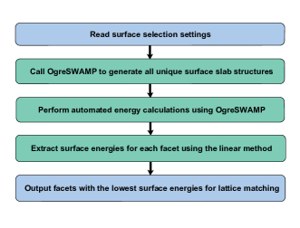
If the substrate orientation is unknown, as in the case of the TTF substrate used by Kattel et al.,Kattel et al. (2017) surface energy calculations may be performed by Ogre. We assume that the most stable facets are the most likely substrate orientations because they are the largest facets in the Wulff shape.Yang et al. (2020) The workflow of the surface selection step is shown in Figure 2. In order to streamline the calculation of surface energies, Ogre is accompanied by the OgreSWAMP utilitiesYang et al. (2020). OgreSWAMP determines the Miller indices of all unique surfaces up to a user-defined maximum Miller index based on the space group symmetries of a given a molecular crystal structure. Automated DFT calculations are performed to obtain the total energy of surface slab models with an increasing number of layers. The surface energy is then calculated using the linear methodScholz and Stirner (2019); Sun and Ceder (2013):
| (2) |
where is the total energy of the surface slab, , is the number of layers in the slab, and is the slab surface area. The energy of the bulk crystal, , and the surface energy, , are extracted from the slope and intercept, respectively.
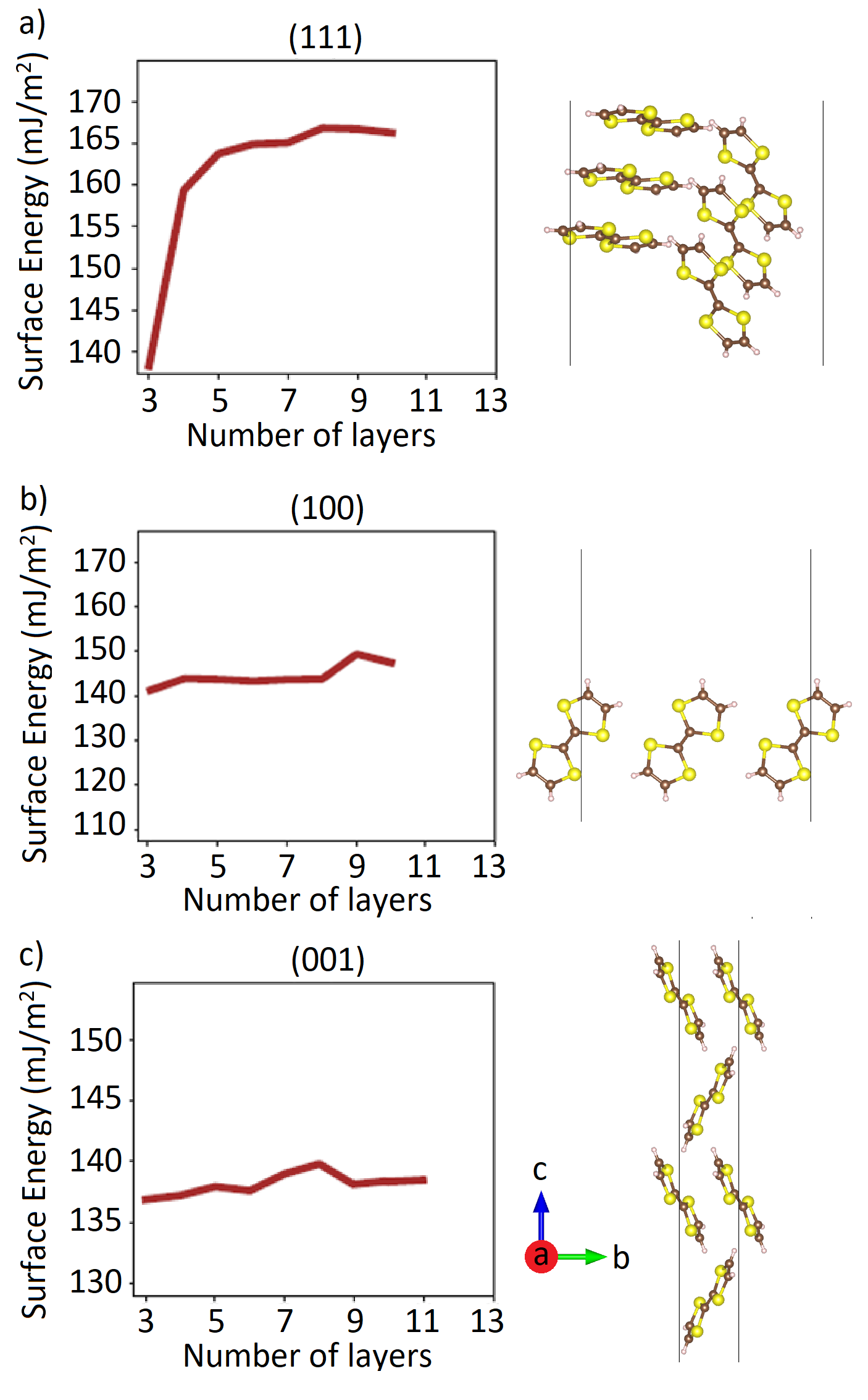
Figure 3 shows the convergence of the surface energy with the number of layers for the (111), (001), and (100) facets of TTF. All other unique surfaces are shown in the SI. The stability of molecular crystal surfaces may be attributed to the chemical groups exposed on the surface.Yang et al. (2020) The (111) facet, shown in Figure 3a, cleaves through the strong interactions in stacking direction of the TTF moleculesAntonijević et al. (2019) and exposes the electron-rich -system and the sulfur atoms of TTF on the surface. Therefore, this facet has a relatively high surface energy. In contrast, the (001) and (100) planes, shown in Figure 3b,c, cleave through a direction nearly perpendicular to the stacking direction of the TTF molecules, exposing hydrogen atoms on the surface. This produces more stable surfaces with lower surface energies. Table 1 summarizes the surfaces energies obtained for all nine unique facets of TTF with a maximal Miller index of 1. The three facets with the lowest surface energies, (001), (100), and (011), were selected for the surface matching step.
| Substrate (TTF) Miller index | Surface energy (mJ/) |
|---|---|
| 001 | 137.901 |
| 100 | 144.843 |
| 011 | 148.198 |
| 01 | 150.802 |
| 11 | 153.019 |
| 010 | 153.754 |
| 110 | 164.103 |
| 111 | 164.117 |
| 101 | 182.249 |
III.3 Lattice Matching
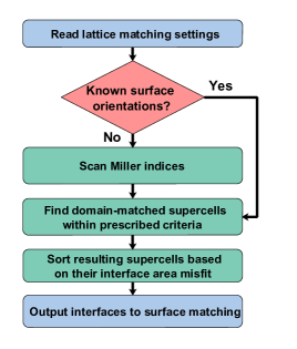
Figure 4 show the workflow of Ogre’s lattice matching step. Lattice matching is controlled by the following input parameters: the substrate and film Miller indices, the maximum interface super-cell area, and the misfit tolerance for the (surface) lattice parameters, surface area, and angles. For organic interfaces, all misfit tolerances are set at 5% by default, and the maximum super-cell area is set at 1000 Å2. ASE is used to obtain the basis vectors of the substrate and film surfaces by cleaving the bulk crystal structures along the specified Miller planes. In order to compare substrate and film two-dimensional lattices using a unique representation, the surface basis vectors are reduced to a pair of primitive basis vectors using Pymatgen. Next, all transformation matrices that would produce lattice matched super-cells within the user-defined tolerance of lattice vector length and angle misfit are constructed using the Pymatgen substrate analyzer module. Finally, all unique commensurate interfaces of a particular system are identified using a reduction scheme and the interface structure is generated. The user may choose to apply strain to either the substrate or the film, however in order to simulate an epitaxial growth experiment, the substrate’s lattice parameter is fixed by default and the film layer is strained to conform to the substrate.
In order to build a lattice matched interface, Ogre generates the matching substrate and film super-cells and aligns the atomic coordinates. The required parameters for creating the interface model, including the interfacial distance, the initial shift in the plane, the number of layers, and the length of the vacuum region can be determined by the user. By default, the interfacial distance and vacuum region and are set to 2 Å and 40 Å, respectively. The initial interface structure has no shifts applied by default. The user may determine the substrate and film thickness by specifying the number of layers or a range of values to calculate. Ogre can detect all possible surface terminations for each Miller plane and automatically generate the corresponding interfaces. The models constructed by Ogre are subsequently used for the surface matching step.
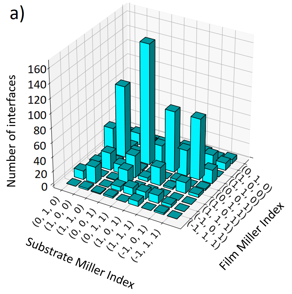
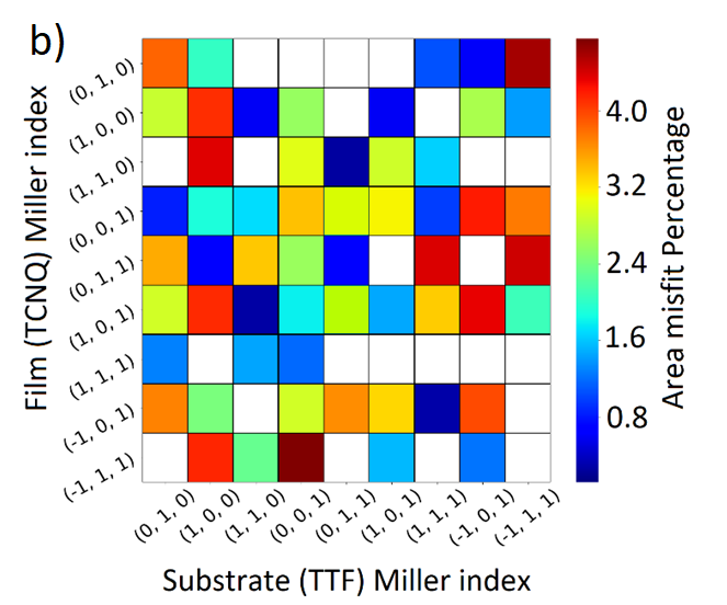
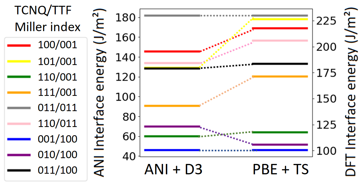
The user may specify the substrate and film Miller indices. If multiple substrate orientations are feasible, and/or the film orientation is unknown Ogre may conduct a Miller index scan, where for each combination of substrate and film Miller indices lattice matching is performed. The input of the Miller index search module is the maximal single index. Ogre enumerates all possible symmetrically unique Miller indices as described in Ref. Yang et al. (2020). For example, the results of a Miller index scan for a TCNQ/TTF interface with a maximal Miller index of 1, a misfit tolerance of 5%, and a maximum area of 1000 Å2 are shown in Figure 5. Panel (a) displays a histogram of the number of domain-matched interfaces generated for each combination of Miller indices. In total, 965 candidate interfaces are generated with these settings. Additional candidate interfaces may be generated by selecting higher misfit tolerances or a larger maximum area, however, they are likely to be less stable. Panel (b) shows the minimum misfit percentage obtained for each interface orientation. Out of 81 possible Miller index combinations, 57 have a misfit under 5%. To narrow down the number of candidates, only the three most stable facets of the TTF substrate, (100), (001), and (011), and only TCNQ facets that lead to an interface with a misfit lower than 2.5 % are considered further. These leave 9 candidate interfaces that proceed to surface matching.
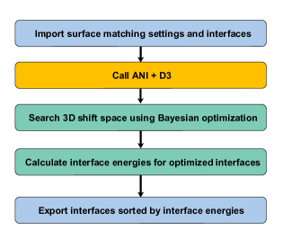
III.4 Surface Matching
Domain-matched interfaces proceed from the lattice matching step to the surface matching step, whose workflow is shown in Figure 6. The optimal position of the film above the substrate is determined using Bayesian optimization (BO) to efficiently search the 3D parameter space of the film position on top of the substrate in the , , and directions. To evaluate the BO objective function, the user may choose DFT or ANI+D3. Ogre provides a grid search option that can generate potential energy surfaces or binding energy curves. Surface matching produces a list of structures ranked by the ANI+D3 interface energy. The final optimized interface structures are exported in the appropriate geometry file format (e.g., geometry.in for FHI-aims).
III.4.1 Performance of ANI+D3
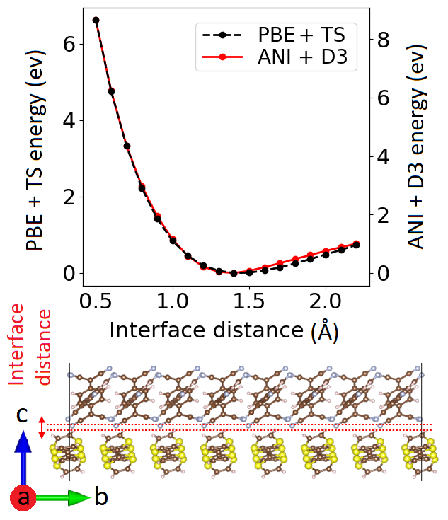
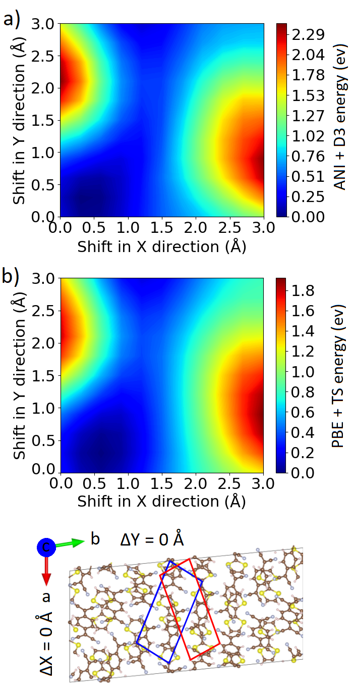
To validate the performance of ANI+D3, we compare its results to DFT, using PBE+TS, for a representative interface structure of TCNQ(110)/TTF(011), illustrated in Figure 7. This structure was selected because it has the lowest area mismatch of 0.23% , as shown in Figure 5. Figure 7 shows a comparison of the potential energy curves as a function of the interfacial distance, obtained with ANI+D3 and PBE+TS. Both curves are referenced to their respective minima. Excellent agreement is demonstrated between ANI+D3 and PBE+TS for the position of the minimum and the shape of the curve. This is possibly because the interfacial distance is dominated by dispersion interactions, whose description by the TS and D3 pairwise methods is similar. Figure 8 shows contour plots of the energy as a function of the position of the TCNQ film on top of the TTF substrate in the plane at a fixed interface distance of 1.4 Å, obtained with ANI+D3 compared with PBE+TS. ANI+D3 agrees well with the positions of the extrema and the features of the DFT potential energy surface. The in-plane registry depends mainly on the local electrostatic and exchange-correlation contributions because the dispersion contribution does not vary significantly at a fixed interfacial distance (a comparison of ANI to PBE without dispersion corrections is provided in the Fig. S3. Hence, the good agreement between ANI+D3 and PBE+TS may be attributed to the fact that ANI is trained to reproduce DFT data for local, intramolecular bonds.
III.4.2 Bayesian Optimization
Bayesian optimization is a machine learning algorithm designed to find the extremum of a "black box" objective function with a minimal number of function queries.Frazier (2018a) Based on the sampled points, a Gaussian process is typically used to construct a statistical model of the objective function, known as the prior.Brochu, Cora, and De Freitas (2010) The following point to be sampled is then determined by an acquisition function. The prior is subsequently updated based on the newly learned information to create a new surrogate model, known as the posterior. The posterior serves as the new prior for the subsequent iteration and so on, until convergence is reached or a predetermined number of steps have been performed.
The BO objective function for surface matching is defined as the negative of the total energy of the interface, calculated using either ANI+D3 or DFT, such that the energy is minimized by maximizing the objective function. Ogre uses the upper confidence bound acquisition functionFrazier (2018b); Brochu, Cora, and De Freitas (2010); Williams and Rasmussen (2006):
| (3) |
where and are the mean and standard deviation at each sampled point. The trade-off between exploitation and exploration is balanced by the hyperparameter . The higher the value of , the more exploration of regions with a high uncertainty is performed. A lower value of accelerates convergence by favoring exploitation of promising regions, however if is too low the BO might converge prematurely to a local extremum.
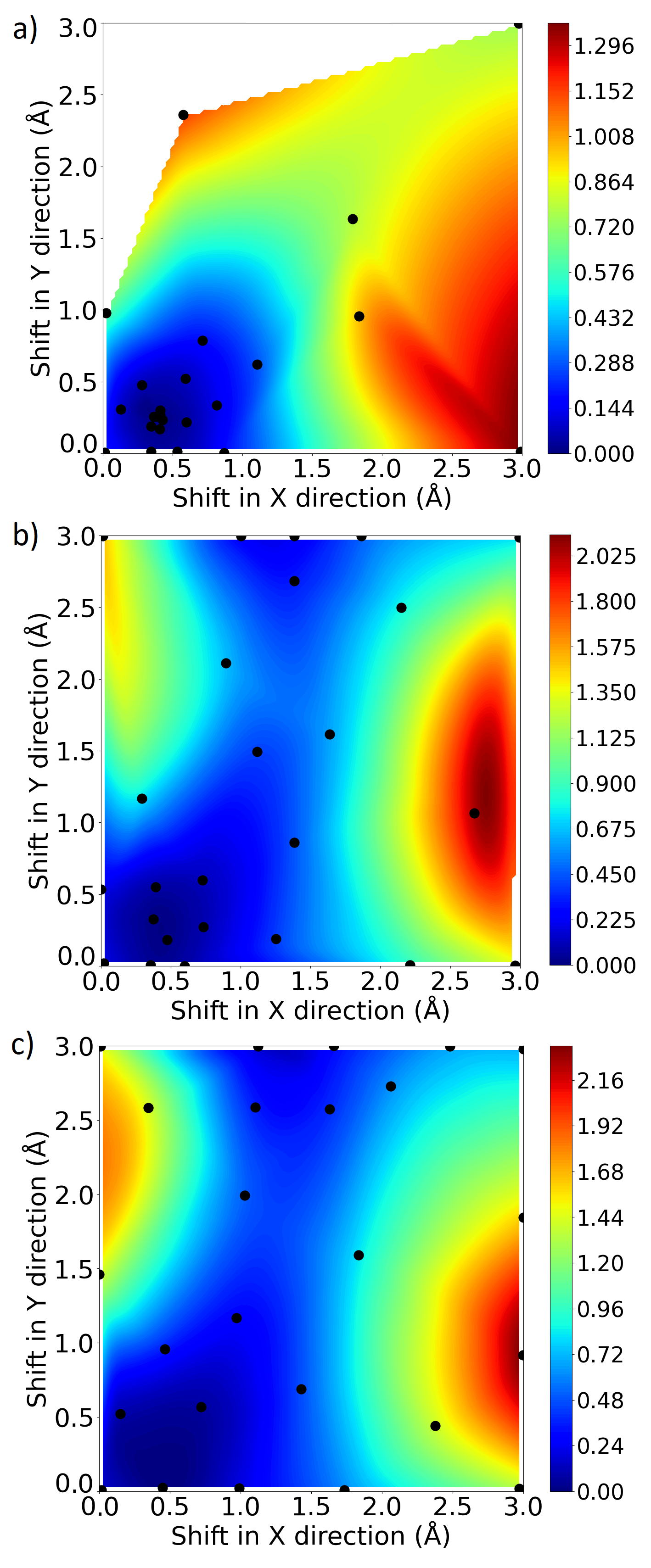
Figure 9 illustrates the effect of the choice of on the BO behavior for the two-dimensional surface of the TCNQ(110)/TTF(011) interface registry in the plane at a fixed interfacial distance of 1.4 Å. With =1 the BO algorithm converges to the global minimum very fast. Nearly all the points sampled are in the vicinity of the minimum and there is very little information on the remainder of the potential energy surface. The Gaussian process predicted mean bears little resemblance to the true ANI+D3 PES, shown in Figure 8a, and the local minimum at (1.25,3.0) is not found. With =5 the BO algorithm performs more exploration of the PES, while still converging relatively quickly to the global minimum. The Gaussian process predicted mean appears more similar to the true PES and the region of the local minimum is also sampled. With =10 significant exploration of the PES is performed, including the regions of the global and local maxima. As a result, the Gaussian process predicted mean appears very similar to the true PES. However, because computer time is wasted on exploring irrelevant regions of the PES, the convergence to the global minimum is slower. For the values of 1 and 5 the BO started to exploit the global minimum region after 11 and 18 iterations, respectively. In comparison, for the value of 10 it took over 25 iterations for the exploitation of the global minimum region to begin, although most of the sampled points were from the lower energy regions. Thus, =5 provides an optimal balance between exploration and exploitation.
The bayesian-optimization Python packageNogueira (2014) is used by Ogre to perform BO. The bounds for shifts in the , ,and directions define the parameter space to be searched. These bounds have default values of (0, ), (0, ), and ( Å, Å), respectively, where and are the interface lattice parameters in the plane and is the initial interface distance. The default values for the number of iterations, N, and are 100 and 5, respectively. The surface matching settings file enables the user to input different parameters than the default values. The most stable interface structure and any structures whose total energy is within a user-defined tolerance of the minimum are output by Ogre once the maximum number of BO iterations has been reached.
BO is significantly more efficient than a grid search because it samples fewer points while maximizing the amount of information learned about the objective function. For example, for the TCNQ(110)/TTF(011) interface with a lattice parameter of 19.4 Å, a grid search with a step size of 0.2 Å and a 1 Å range for the axis would require evaluating more than 47000 points. In comparison, the BO algorithm converges to the optimal interface configuration within 300 iterations. The computational cost of performing BO amounts to the number of sampled points multiplied by the cost of the objective function evaluation, which is the cost of an energy calculation with either ANI+D3 or DFT. ANI+D3 is faster than DFT by orders of magnitude. For example, single point energy evaluations for the TCNQ(110)/TTF(011) interface took about 7 s using ANI+D3, compared to about 4000 s using DFT (PBE+TS).
III.5 Ranking
Every interface structure passed from the lattice matching step is surface matched, which could result in a significant number of candidate structures. Fast preliminary ranking is performed with ANI+D3 in order to down-select a smaller group of the most promising candidate structures for the final evaluation with DFT. The interface energy, , is defined as the energy required to eliminate two surfaces and form an interface: Xiong et al. (2017); Christensen, Dudiy, and Wahnström (2002); Moayedpour et al. (2021); Dardzinski et al. (2022)
| (4) |
where, is the interface adhesive energy and are the surface energies of the substrate and film, calculated using Eq. 2,Yang et al. (2020) The adhesive energy of an interface is defined as:Li et al. (2016); Liu, Wang, and Ye (2004); Zhuo et al. (2018); Wang, Li, and Xu (2020)
| (5) |
where , , and are total energies of the substrate surface slab, the film surface slab, and the interface, respectively. , , and may be evaluated using either ANI+D3 or DFT. For inorganic interfaces, we have proposed a linear method for converging the interface energy as a function of the number of layers.Moayedpour et al. (2021); Dardzinski et al. (2022) For organic interfaces it is not feasible to calculate the interface energy for models with more than one layer of the substrate and one layer of the film, owing to the large system size. With only one layer of substrate and film, the smallest interface studied here, TCNQ(110)/TTF(011), contains 777 atoms and the largest interface studied here, TCNQ(111)/TTF(001), contains 1655 atoms. In addition, the thickness of these organic interface models ranges from 93.58 Å for TCNQ(110)/TTF(011) to 109.15 Å for TCNQ(100)/TTF(001), which is roughly equivalent to an inorganic interface with 40 atomic layers. Owing to the weak nature of the dispersion interactions at organic interfaces and their large size, it is therefore a reasonable approximation to calculate the interface energy for models with only one layer of the substrate and one layer of the film.
In figure 10 the interfaces energies obtained with ANI+D3 are compared to DFT interface energies obtained with PBE+TS for the TCNQ/TTF interfaces with the lowest substrate surface energies and interface area misfit. Because the ANI potentials have been trained on isolated molecules and have never "seen" an interface, we do not expect the interface energy values to be in close agreement with DFT values. Nevertheless, the ranking obtained with ANI+D3 is in reasonable agreement with the DFT ranking in the sense that the group of most stable structures is correctly identified. Hence we have confidence in the preliminary raking with ANI+D3 as a method of narrowing down the number of candidate structures to be calculated with DFT.
III.6 Electronic Structure
We now proceed to study the electronic structure of the two most stable interface configurations of TCNQ(001)/TTF(100) and TCNQ(010)/TTF(100). Previously, Beltrán et al. conducted DFT simulations of the TCNQ/TTF interface, whose structure was derived from a TTF-TCNQ co-crystal.Beltrán et al. (2013) However, the structure of the co-crystal is significantly different than the bulk structure of either material. Therefore, such a model is not appropriate for the epitaxial growth of TCNQ on top of TTF by Kattel et al.Kattel et al. (2017) Beltrán et al. used the local density approximation (LDA), with an empirical correction of the interface energy level alignment to compensate for the severe underestimation of band gaps by the LDA. Here, we use the HSE hybrid functional, which contains 25% of exact (Fock) exchange. Atalla et al. have shown for an isolated dimer of TTF and TCNQ molecules that a larger fraction of exact exchange is required to reproduce the correct energy level alignment.Atalla et al. (2016); Park et al. (2017) However, in extended systems the energy level alignment changes owing to band dispersion and polarization-induced gap narrowing.Wang et al. (2019) Hence, the HSE functional provides a correct description of the energy level alignment and the charge transfer at the interface of TTF and TCNQ, as we demonstrate below.
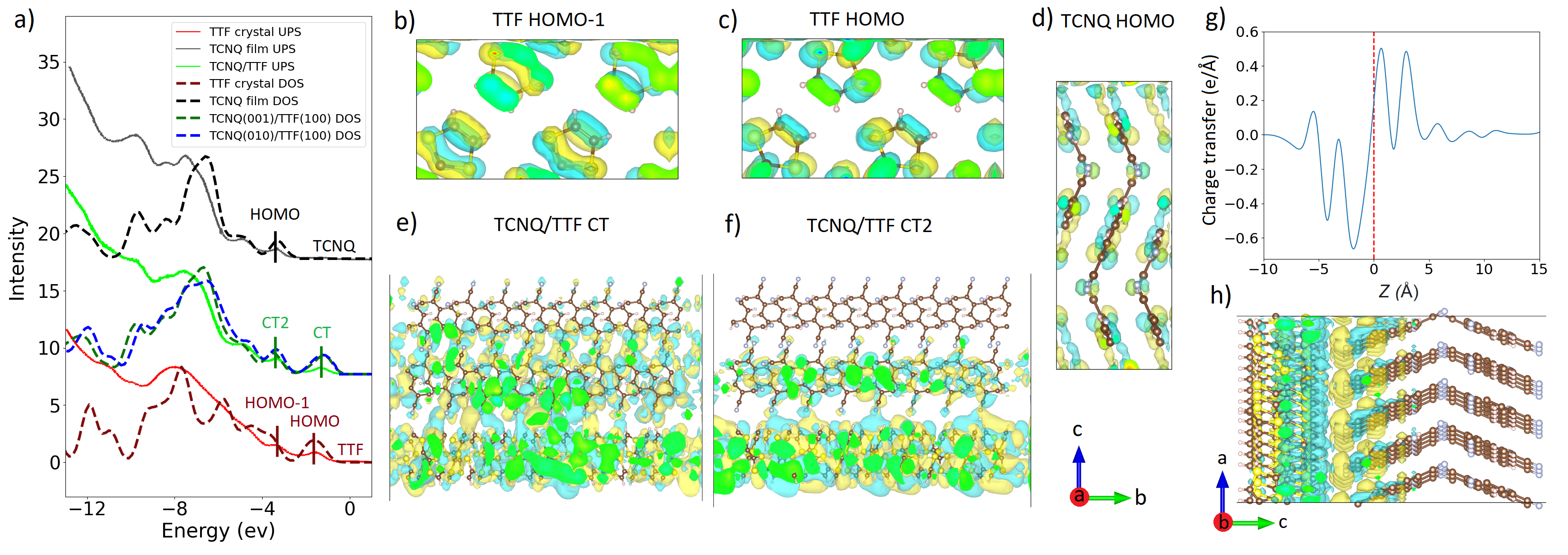
Kattle et al. conducted UPS experiments for TCNQ films ranging in thickness from 0.3 nm to 10 nm, deposited on a single crystal of TTF.Kattel et al. (2017) In our model of the of TCNQ(001)/TTF(100) interface with a single layer of each material the thickness of the TCNQ film is 1.653 nm. Therefore, we compare our results to the UPS result of the 1 nm thick TCNQ film. The UPS results of bulk TTF and TCNQ are compared to calculations conducted for the respective crystals. Figure 11a shows the comparison of the computed density of states (DOS) with UPS experiments. The absolute energies of the Kohn-Sham orbitals from ground state DFT calculations using approximate exchange-correlation functionals do not strictly correspond to ionization energies.Kronik and Kümmel (2014) Therefore, the computed DOS are shifted to align the first peak with the first UPS peak. In addition Gaussian broadening of 0.1 eV is applied to the DOS to simulate the resolution of the experiment. The comparison between theory and experiment is focused only on peak positions. We do not consider the secondary electron background, which leads to the increase of the spectral intensity towards lower binding energies,Kattel et al. (2017) vibrational effects, or intensity variations due to the scattering cross-section and penetration depth.Ueno and Kera (2008) The positions of the peaks in the DOS of the TTF crystal, the TCNQ crystal, and the TCNQ/TTF interface are in a good agreement with the position of the peaks in the UPS spectra. The DOS of the TTF(100)/TCNQ(001) and the TCNQ(010)/TTF(100) interface structures are similar with the TTF(100)/TCNQ(001) DOS being in slightly better agreement with experiment. An experiment with a finer resolution may be required to unambiguously determine the interface structure.
In the spectrum of the interface with the 1 nm thick TCNQ film, the peak observed around -1.5 eV was attributed by Kattle et al. to a CT state, which is likely responsible for the high conductivity of the interface. Indeed, in our DFT simulations, the interface exhibits metallic behavior. Owing to the number of molecules included in the interface models, several orbitals contribute to each peak in the computed DOS. Within a 0.01 eV energy range of the peaks centers, 7 orbitals contribute to the first peak and 9 orbitals contribute to the second peak. The orbitals with energies closest to the peak centeres are depicted in 11 The first peak, labeled CT, originates from a state that is delocalized over the interface and is distinct from the HOMO of TTF, as shown in Figure 11. We attribute this interface state to ground state CT from TTF to TCNQ, rather than a CT excitation, in agreement with experiment. Kattle et al. estimated the spatial extent of the CT state to be 1-2 nm or less, which is in agreement with our simulation. The second peak in the DOS of the interface, labeled CT2, arises from a delocalized state across the interface, comprising mixed contributions from the TTF HOMO-1 and the TCNQ HOMO, which are close in energy. The charge transfer at the TCNQ(001)/TTF(100) interface is given by the difference between the DFT charge density of the interface and the charge densities of isolated substrate and bulk slabs with the same geometryYang, Wu, and Marom (2020):
| (6) |
where the charge is averaged over the plane at each position along the -axis. Figure 11f-g shows the charge transfer as a function of position across the interface. The net charge is negative at the interfacial layer of TTF(100) and positive at the TCNQ(001) layer, which confirms that the charge is transferred from the TTF substrate to the TCNQ film.
IV Conclusion
We have presented a method for structure prediction of epitaxial organic interfaces by lattice and surface matching, implemented in the Ogre open-source Python package. The lattice matching step identifies all potential domain-matched interface super-cells within user-defined tolerances for interface area and lattice mismatch. The most stable facets of the substrate may be pre-selected by calculating the surface energies. If several substrate and/or film orientations are possible, a Miller index scan may be performed to find the combinations that result in the best candidate interface structures.
In the surface matching step, Bayesian optimization (BO) is utilized to determine the optimal configuration of each domain-matched interface in terms of the interfacial distance in the direction and the registry in the plane. The BO objective function is based on the energy of the interface evaluated using the ANI deep neural network inter-atomic potentials with the Grimme D3 dispersion correction. ANI+D3 successfully reproduces the DFT results for the energy as a function of the interfacial distance and the features of the DFT potential energy surface in the plane at a fraction of the computational cost. In addition, the preliminary ranking of interface structures with ANI+D3 is in reasonable agreement with the DFT ranking and the most stable interface structures are correctly identified. DFT simulations can be performed for a small number of the most promising candidate interface structures. Ogre streamlines the construction of surface and interface slab models.
The application of Ogre has been demonstrated for an epitaxial interface of TCNQ on TTF, which is of interest for organic electronics. The electronic structure of the TCNQ/TTF interface had been probed by UPS, however its structure had not been experimentally characterized. The three facets of the TTF substrate with the lowest surface energies were found to be (001), (100), and (011). The stability of these surfaces may be attributed to the H-terminated edges of the TTF molecules being exposed on the surface, rather than the system in the plane of the rings. A Miller index scan was performed to identify the TCNQ film orientations that lead to interfaces with the lowest lattice mismatch. Nine interfaces with different Miller index combinations were selected for surface matching. In the final ranking, TCNQ(001)/TTF(100) was found to be the most stable interface configuration followed by TCNQ(010)/TTF(100). Electronic structure calculations were performed for both of these interfaces and compared with UPS experiments. Excellent agreement was obtained between the computed DOS and UPS measurements in terms of the relative peak positions, although experiments with higher resolution would be required to unambiguously distinguish between the TCNQ(001)/TTF(100) and TCNQ(010)/TTF(100) interface configurations. For the most stable TCNQ(001)/TTF(100) interface configuration, we have also investigated the charge transfer. The first peak of the spectrum of the interface was found to be associated with an orbital delocalized over the interface, rather than states belonging to either the TTF or TCNQ. Ground state charge transfer from TTF to TCNQ was observed in agreement with experiment.
In conclusion, we have shown that Ogre can contribute to advancements in the understanding of the structure and properties of epitaxial organic interfaces. Ogre can help interpret experiments by predicting the most likely interface configurations and correlating the structures with observed spectral features. Furthermore, Ogre may guide experimental growth efforts of epitaxial organic interfaces by identifying material combinations that are likely to form high-quality interfaces. In the future, Ogre may be integrated into automated materials discovery workflows to enable the computational design and discovery of epitaxial organic interfaces for high-performance organic electronic devices.
Acknowledgements.
We thank Wai-Lun Chan from the University of Kansas and Barry Rand from Princeton University for helpful discussions. Funding was provided by the U.S. Army Research Office (ARO) under grant W911NF1810148. O.I. acknowledges the Office of Naval Research (ONR) through support provided by the Energetic Materials Program (MURI grant no. N00014-21-1-2476). This research used resources of the National Energy Research Scientific Computing Center (NERSC), a DOE Office of Science User Facility supported by the Office of Science of the U.S. Department of Energy, under Contract DE-AC02-05CH11231. This work used the Extreme Science and Engineering Discovery Environment (XSEDE), which is supported by National Science Foundation grant number ACI-1548562.References
- Mazzio and Luscombe (2014) K. A. Mazzio and C. K. Luscombe, “The future of organic photovoltaics,” Chemical Society Reviews 44, 78–90 (2014).
- Kippelen and Brédas (2009) B. Kippelen and J.-L. Brédas, “Organic photovoltaics,” Energy Environ. Sci. 2, 251–261 (2009).
- Reineke et al. (2013) S. Reineke, M. Thomschke, B. Lüssem, and K. Leo, “White organic light-emitting diodes: Status and perspective,” Rev. Mod. Phys. 85, 1245–1293 (2013).
- Liu et al. (2018) Y. Liu, C. Li, Z. Ren, S. Yan, and M. R. Bryce, “All-organic thermally activated delayed fluorescence materials for organic light-emitting diodes,” Nature Reviews Materials 3, 1–20 (2018).
- Brütting, Berleb, and Mückl (2001) W. Brütting, S. Berleb, and A. G. Mückl, “Device physics of organic light-emitting diodes based on molecular materials,” Organic Electronics 2, 1–36 (2001).
- Armstrong et al. (2009) N. R. Armstrong, W. Wang, D. M. Alloway, D. Placencia, E. Ratcliff, and M. Brumbach, “Organic/organic heterojunctions: Organic light emitting diodes and organic photovoltaic devices,” Macromolecular Rapid Communications 30, 717–731 (2009).
- Mas-Torrent and Rovira (2011) M. Mas-Torrent and C. Rovira, “Role of molecular order and solid-state structure in organic field-effect transistors,” Chemical Reviews 111, 4833–4856 (2011).
- Chen et al. (2020) H. Chen, W. Zhang, M. Li, G. He, and X. Guo, “Interface engineering in organic field-effect transistors: Principles, applications, and perspectives,” Chemical Reviews 120, 2879–2949 (2020).
- Sirringhaus (2014) H. Sirringhaus, “25th anniversary article: Organic field-effect transistors: The path beyond amorphous silicon,” Advanced Materials 26, 1319–1335 (2014).
- Braga and Horowitz (2009) D. Braga and G. Horowitz, “High-performance organic field-effect transistors,” Advanced Materials 21, 1473–1486 (2009).
- Wang et al. (2022) S.-J. Wang, M. Sawatzki, G. Darbandy, F. Talnack, J. Vahland, M. Malfois, A. Kloes, S. Mannsfeld, H. Kleemann, and K. Leo, “Organic bipolar transistors,” Nature 606, 700–705 (2022).
- Khan and Rand (2021) S.-U.-Z. Khan and B. P. Rand, “Influence of disorder and state filling on charge-transfer-state absorption and emission spectra,” Phys. Rev. Applied 16, 044026 (2021).
- Khan et al. (2019) S.-U.-Z. Khan, G. Londi, X. Liu, M. A. Fusella, G. D’Avino, L. Muccioli, A. N. Brigeman, B. Niesen, T. C.-J. Yang, Y. Olivier, J. T. Dull, N. C. Giebink, D. Beljonne, and B. P. Rand, “Multiple charge transfer states in donor–acceptor heterojunctions with large frontier orbital energy offsets,” Chemistry of Materials 31, 6808–6817 (2019).
- Choi et al. (2020) H. H. Choi, A. F. Paterson, M. A. Fusella, J. Panidi, O. Solomeshch, N. Tessler, M. Heeney, K. Cho, T. D. Anthopoulos, B. P. Rand, and V. Podzorov, “Hall effect in polycrystalline organic semiconductors: The effect of grain boundaries,” Advanced Functional Materials 30, 1903617 (2020).
- Gershenson, Podzorov, and Morpurgo (2006) M. E. Gershenson, V. Podzorov, and A. F. Morpurgo, “Colloquium: Electronic transport in single-crystal organic transistors,” Rev. Mod. Phys. 78, 973–989 (2006).
- Coropceanu et al. (2007) V. Coropceanu, J. Cornil, D. A. da Silva Filho, Y. Olivier, R. Silbey, and J.-L. Brédas, “Charge transport in organic semiconductors,” Chemical Reviews 107, 926–952 (2007).
- Nakayama, Kera, and Ueno (2020) Y. Nakayama, S. Kera, and N. Ueno, “Photoelectron spectroscopy on single crystals of organic semiconductors: experimental electronic band structure for optoelectronic properties,” J. Mater. Chem. C 8, 9090–9132 (2020).
- Podzorov (2013) V. Podzorov, “Organic single crystals: Addressing the fundamentals of organic electronics,” MRS Bulletin 38, 15–24 (2013).
- Li et al. (2010) R. Li, W. Hu, Y. Liu, and D. Zhu, “Micro- and nanocrystals of organic semiconductors,” Accounts of Chemical Research 43, 529–540 (2010).
- Reese and Bao (2007) C. Reese and Z. Bao, “Organic single-crystal field-effect transistors,” Materials Today 10, 20–27 (2007).
- Fusella et al. (2018) M. A. Fusella, A. N. Brigeman, M. Welborn, G. E. Purdum, Y. Yan, R. D. Schaller, Y. H. L. Lin, Y. L. Loo, T. V. Voorhis, N. C. Giebink, and B. P. Rand, “Band-like Charge Photogeneration at a Crystalline Organic Donor/Acceptor Interface,” Advanced Energy Materials 8, 1701494 (2018).
- Raimondo et al. (2011) L. Raimondo, M. Moret, M. Campione, A. Borghesi, and A. Sassella, “Unique orientation of organic epitaxial thin films: The role of intermolecular interactions at the interface and surface symmetry,” Journal of Physical Chemistry C 115, 5880–5885 (2011).
- Schreiber (2004) F. Schreiber, “Organic molecular beam deposition: Growth studies beyond the first monolayer,” Physica Status Solidi (a) 201, 1037–1054 (2004).
- Forrest et al. (1994) S. R. Forrest, P. E. Burrows, E. I. Haskal, and F. F. So, “Ultrahigh-vacuum quasiepitaxial growth of model van der Waals thin films. II. Experiment,” Physical Review B 49, 11309 (1994).
- Moret et al. (2011) M. Moret, A. Borghesi, M. Campione, E. Fumagalli, L. Raimondo, and A. Sassella, “Organic-organic heteroepitaxy: facts, concepts and perspectives,” Crystal Research and Technology 46, 827–832 (2011).
- Sassella (2013) A. Sassella, “Organic epitaxial layers on organic substrates,” Crystal Research and Technology 48, 840–848 (2013).
- Koma (1995) A. Koma, “Molecular beam epitaxial growth of organic thin films,” Progress in Crystal Growth and Characterization of Materials 30, 129–152 (1995).
- Koma (1999) A. Koma, “Van der Waals epitaxy for highly lattice-mismatched systems,” Journal of Crystal Growth 201-202, 236–241 (1999).
- Fenter et al. (1997) P. Fenter, F. Schreiber, L. Zhou, P. Eisenberger, and S. Forrest, “In situ studies of morphology, strain, and growth modes of a molecular organic thin film,” Physical Review B 56, 3046–3053 (1997).
- Forrest and Zhang (1994) S. R. Forrest and Y. Zhang, “Ultrahigh-vacuum quasiepitaxial growth of model van der Waals thin films. I. Theory,” Physical Review B 49, 11297 (1994).
- Hooks, Fritz, and Ward (2001) D. E. Hooks, T. Fritz, and M. D. Ward, “Epitaxy and molecular organization on solid substrates,” Advanced Materials 13, 227–241 (2001).
- Yang and Yan (2009) J. Yang and D. Yan, “Weak epitaxy growth of organic semiconductor thin films,” Chem. Soc. Rev. 38, 2634–2645 (2009).
- Yang, Yan, and Jones (2015) J. Yang, D. Yan, and T. S. Jones, “Molecular Template Growth and Its Applications in Organic Electronics and Optoelectronics,” Chemical Reviews 115, 5570–5603 (2015).
- Forrest (1997) S. R. Forrest, “Ultrathin organic films grown by organic molecular beam deposition and related techniques,” Chemical Reviews 97, 1793–1896 (1997).
- Campione et al. (2009) M. Campione, L. Raimondo, M. Moret, P. Campiglio, E. Fumagalli, and A. Sassella, “Organic-organic heteroepitaxy of semiconductor crystals: -quaterthiophene on rubrene,” Chemistry of Materials 21, 4859–4867 (2009).
- Al-Mahboob et al. (2009) A. Al-Mahboob, J. T. Sadowski, Y. Fujikawa, and T. Sakurai, “The growth mechanism of pentacene-fullerene heteroepitaxial films,” Surface Science 603, L53–L56 (2009).
- Nakayama et al. (2016) Y. Nakayama, Y. Mizuno, T. Hosokai, T. Koganezawa, R. Tsuruta, A. Hinderhofer, A. Gerlach, K. Broch, V. Belova, H. Frank, M. Yamamoto, J. Niederhausen, H. Glowatzki, J. P. Rabe, N. Koch, H. Ishii, F. Schreiber, and N. Ueno, “Epitaxial growth of an organic p-n heterojunction: C60 on single-crystal pentacene,” ACS Applied Materials and Interfaces 8, 13499–13505 (2016).
- Nakayama et al. (2018) Y. Nakayama, R. Tsuruta, A. Hinderhofer, Y. Mizuno, K. Broch, A. Gerlach, T. Koganezawa, T. Hosokai, and F. Schreiber, “Temperature dependent epitaxial growth of C60 overlayers on single crystal pentacene,” Advanced Materials Interfaces 5, 1800084 (2018).
- Conrad et al. (2009) B. R. Conrad, J. Tosado, G. Dutton, D. B. Dougherty, W. Jin, T. Bonnen, A. Schuldenfrei, W. G. Cullen, E. D. Williams, J. E. Reutt-Robey, and S. W. Robey, “C60 cluster formation at interfaces with pentacene thin-film phases,” Applied Physics Letters 95, 213302 (2009).
- Huttner, Breuer, and Witte (2019) A. Huttner, T. Breuer, and G. Witte, “Controlling interface morphology and layer crystallinity in organic heterostructures: Microscopic view on c60 island formation on pentacene buffer layers,” ACS Applied Materials and Interfaces 11, 35177–35184 (2019).
- Iwasawa et al. (2020) M. Iwasawa, R. Tsuruta, Y. Nakayama, M. Sasaki, T. Hosokai, S. Lee, K. Fukumoto, and Y. Yamada, “Exciton dissociation and electron transfer at a well-defined organic interface of an epitaxial C60 layer on a pentacene single crystal,” The Journal of Physical Chemistry C 124, 13572–13579 (2020).
- Mitsuta et al. (2017) H. Mitsuta, T. Miyadera, N. Ohashi, Y. Zhou, T. Taima, T. Koganezawa, Y. Yoshida, and M. Tamura, “Epitaxial growth of C60 on rubrene single crystals for a highly ordered organic donor/acceptor interface,” Crystal Growth & Design 17, 4622–4627 (2017).
- Nakayama et al. (2019) Y. Nakayama, R. Tsuruta, N. Moriya, M. Hikasa, M. Meissner, T. Yamaguchi, Y. Mizuno, T. Suzuki, T. Koganezawa, T. Hosokai, T. Ueba, and S. Kera, “Widely dispersed intermolecular valence bands of epitaxially grown perfluoropentacene on pentacene single crystals,” The Journal of Physical Chemistry Letters 10, 1312–1318 (2019).
- Hinderhofer et al. (2011) A. Hinderhofer, T. Hosokai, C. Frank, J. Novák, A. Gerlach, and F. Schreiber, “Templating effect for organic heterostructure film growth: Perfluoropentacene on diindenoperylene,” Journal of Physical Chemistry C 115, 16155–16160 (2011).
- Barrena et al. (2006) E. Barrena, D. G. De Oteyza, S. Sellner, H. Dosch, J. O. Osso, and B. Struth, “In situ study of the growth of nanodots in organic heteroepitaxy,” Physical Review Letters 97, 076102 (2006).
- Takahashi et al. (2021) K. Takahashi, S. Izawa, N. Ohtsuka, A. Izumiseki, R. Tsuruta, R. Takeuchi, Y. Gunjo, Y. Nakanishi, K. Mase, T. Koganezawa, N. Momiyama, M. Hiramoto, and Y. Nakayama, “Quasi-homoepitaxial junction of organic semiconductors: A structurally seamless but electronically abrupt interface between rubrene and bis(trifluoromethyl)dimethylrubrene,” The Journal of Physical Chemistry Letters 12, 11430–11437 (2021).
- Gunjo et al. (2021) Y. Gunjo, H. Kamebuchi, R. Tsuruta, M. Iwashita, K. Takahashi, R. Takeuchi, K. Kanai, T. Koganezawa, K. Mase, M. Tadokoro, and Y. Nakayama, “Interface structures and electronic states of epitaxial tetraazanaphthacene on single-crystal pentacene,” Materials 14, 1088 (2021).
- Kattel et al. (2017) B. Kattel, T. Wang, T. R. Kafle, and W. L. Chan, “The thickness of the two-dimensional charge transfer state at the TTF-TCNQ interface,” Organic Electronics 48, 371–376 (2017).
- Döring et al. (2019) R. C. Döring, N. W. Rosemann, A. Huttner, T. Breuer, G. Witte, and S. Chatterjee, “Charge-transfer processes and carrier dynamics at the pentacene-C60 interface,” Journal of Physics: Condensed Matter 31, 134001 (2019).
- Dardzinski et al. (2022) D. Dardzinski, M. Yu, S. Moayedpour, and N. Marom, “Best practices for first-principles simulations of epitaxial inorganic interfaces,” Journal of Physics: Condensed Matter 34, 233002 (2022).
- Moayedpour et al. (2021) S. Moayedpour, D. Dardzinski, S. Yang, A. Hwang, and N. Marom, “Structure prediction of epitaxial inorganic interfaces by lattice and surface matching with Ogre,” The Journal of Chemical Physics 155, 034111 (2021).
- Mathew et al. (2016) K. Mathew, A. K. Singh, J. J. Gabriel, K. Choudhary, S. B. Sinnott, A. V. Davydov, F. Tavazza, and R. G. Hennig, “MPInterfaces: A Materials Project based Python tool for high-throughput computational screening of interfacial systems,” Computational Materials Science 122, 183–190 (2016).
- Ding et al. (2016) H. Ding, S. S. Dwaraknath, L. Garten, P. Ndione, D. Ginley, and K. A. Persson, “Computational Approach for Epitaxial Polymorph Stabilization through Substrate Selection,” ACS Applied Materials and Interfaces 8, 13086–13093 (2016).
- Raclariu et al. (2015) A. M. Raclariu, S. Deshpande, J. Bruggemann, W. Zhuge, T. H. Yu, C. Ratsch, and S. Shankar, “A fast method for predicting the formation of crystal interfaces and heterocrystals,” Computational Materials Science 108, 88–93 (2015).
- Sun and Ceder (2013) W. Sun and G. Ceder, “Efficient creation and convergence of surface slabs,” Surface Science 617, 53–59 (2013).
- Gao et al. (2019) B. Gao, P. Gao, S. Lu, J. Lv, Y. Wang, and Y. Ma, “Interface structure prediction via CALYPSO method,” Science Bulletin 64, 301–309 (2019).
- Mannsfeld and Fritz (2011) S. C. Mannsfeld and T. Fritz, “Advanced modelling of epitaxial ordering of organic layers on crystalline surfaces,” Modern Physics Letters B 20, 585–605 (2011).
- Packwood and Hitosugi (2017) D. M. Packwood and T. Hitosugi, “Rapid prediction of molecule arrangements on metal surfaces via Bayesian optimization,” Applied Physics Express 10, 065502 (2017).
- Packwood, Han, and Hitosugi (2017) D. M. Packwood, P. Han, and T. Hitosugi, “Chemical and entropic control on the molecular self-assembly process,” Nature Communications 8, 1–8 (2017).
- Obersteiner et al. (2017) V. Obersteiner, M. Scherbela, L. Hörmann, D. Wegner, and O. T. Hofmann, “Structure Prediction for Surface-Induced Phases of Organic Monolayers: Overcoming the Combinatorial Bottleneck,” Nano Letters 17, 4453–4460 (2017).
- Scherbela et al. (2018) M. Scherbela, L. Hörmann, A. Jeindl, V. Obersteiner, and O. T. Hofmann, “Charting the energy landscape of metal/organic interfaces via machine learning,” Physical Review Materials 2, 043803 (2018).
- Han, Shen, and Yi (2015) G. Han, X. Shen, and Y. Yi, “Deposition growth and morphologies of C60 on DTDCTB surfaces: An atomistic insight into the integrated impact of surface stability, landscape, and molecular orientation,” Advanced Materials Interfaces 2, 1500329 (2015).
- Fu et al. (2014) Y.-T. Fu, D. A. da Silva Filho, G. Sini, A. M. Asiri, S. G. Aziz, C. Risko, and J.-L. Brédas, “Structure and disorder in squaraine–C60 organic solar cells: A theoretical description of molecular packing and electronic coupling at the donor–acceptor interface,” Advanced Functional Materials 24, 3790–3798 (2014).
- Fu, Risko, and Brédas (2013) Y.-T. Fu, C. Risko, and J.-L. Brédas, “Intermixing at the pentacene-fullerene bilayer interface: A molecular dynamics study,” Advanced Materials 25, 878–882 (2013).
- Yoo et al. (2019) D. Yoo, H. Song, Y. Youn, S. H. Jeon, Y. Cho, and S. Han, “A molecular dynamics study on the interface morphology of vapor-deposited amorphous organic thin films,” Phys. Chem. Chem. Phys. 21, 1484–1490 (2019).
- Yang et al. (2020) S. Yang, I. Bier, W. Wen, J. Zhan, S. Moayedpour, and N. Marom, “Ogre: A python package for molecular crystal surface generation with applications to surface energy and crystal habit prediction,” The Journal of Chemical Physics 152, 244122 (2020).
- Zur and McGill (1998) A. Zur and T. C. McGill, “Lattice match: An application to heteroepitaxy,” Journal of Applied Physics 55, 378 (1998).
- Spackman and Jayatilaka (2009) M. A. Spackman and D. Jayatilaka, “Hirshfeld surface analysis,” CrystEngComm 11, 19–32 (2009).
- Smith, Isayev, and Roitberg (2017) J. S. Smith, O. Isayev, and A. E. Roitberg, “ANI-1: an extensible neural network potential with DFT accuracy at force field computational cost,” Chemical Science 8, 3192–3203 (2017).
- Smith et al. (2020) J. S. Smith, R. Zubatyuk, B. Nebgen, N. Lubbers, K. Barros, A. E. Roitberg, O. Isayev, and S. Tretiak, “The ANI-1ccx and ANI-1x data sets, coupled-cluster and density functional theory properties for molecules,” Scientific Data 7, 1–10 (2020).
- Smith et al. (2018) J. S. Smith, B. Nebgen, N. Lubbers, O. Isayev, and A. E. Roitberg, “Less is more: Sampling chemical space with active learning,” The Journal of Chemical Physics 148, 241733 (2018).
- Smith et al. (2016) D. G. Smith, L. A. Burns, K. Patkowski, and C. D. Sherrill, “Revised Damping Parameters for the D3 Dispersion Correction to Density Functional Theory,” Journal of Physical Chemistry Letters 7, 2197–2203 (2016).
- Grimme, Ehrlich, and Goerigk (2011) S. Grimme, S. Ehrlich, and L. Goerigk, “Effect of the damping function in dispersion corrected density functional theory,” Journal of Computational Chemistry 32, 1456–1465 (2011).
- Ehrlich et al. (2011) S. Ehrlich, J. Moellmann, W. Reckien, T. Bredow, and S. Grimme, “System-Dependent Dispersion Coefficients for the DFT-D3 Treatment of Adsorption Processes on Ionic Surfaces,” ChemPhysChem 12, 3414–3420 (2011).
- Murdey and Salaneck (2005) R. J. Murdey and W. R. Salaneck, “Charge injection barrier heights across multilayer organic thin films,” Japanese Journal of Applied Physics 44, 3751–3756 (2005).
- Braun et al. (2010) S. Braun, X. Liu, W. Salaneck, and M. Fahlman, “Fermi level equilibrium at donor–acceptor interfaces in multi-layered thin film stack of ttf and tcnq,” Organic Electronics 11, 212–217 (2010).
- Beltrán et al. (2013) J. I. Beltrán, F. Flores, J. I. Martínez, and J. Ortega, “Energy level alignment in organic-organic heterojunctions: The TTF/TCNQ interface,” Journal of Physical Chemistry C 117, 3888–3894 (2013).
- Atalla et al. (2016) V. Atalla, I. Y. Zhang, O. T. Hofmann, X. Ren, P. Rinke, and M. Scheffler, “Enforcing the linear behavior of the total energy with hybrid functionals: Implications for charge transfer, interaction energies, and the random-phase approximation,” Physical Review B 94, 035140 (2016).
- Ando et al. (2008) T. Ando, A. B. Fowler, F. Stern, T. J. Kistenmacher, T. E. Phillips, D. O. Cowan, A. Endo, Y. Iye, and A. Brinkman, “When TTF met TCNQ,” Nature Materials 7, 520–521 (2008).
- Cohen et al. (1974) M. J. Cohen, L. B. Coleman, A. F. Garito, and A. J. Heeger, “Electrical conductivity of tetrathiofulvalinium tetracyanoquinodimethan (TTF) (TCNQ),” Physical Review B 10, 1298 (1974).
- Ferraris et al. (2002) J. Ferraris, D. O. Cowan, V. Walatka, and J. H. Perlstein, “Electron transfer in a new highly conducting donor-acceptor complex,” Journal of the American Chemical Society 95, 948–949 (2002).
- Alves, Pinto, and MaçÔas (2013) H. Alves, R. M. Pinto, and E. S. MaçÔas, “Photoconductive response in organic charge transfer interfaces with high quantum efficiency,” Nature Communications 4, 1842 (2013).
- Krupskaya et al. (2016) Y. Krupskaya, F. Rückerl, M. Knupfer, A. F. Morpurgo, Y. Krupskaya, A. F. Morpurgo, F. Rückerl, and M. Knupfer, “Charge Transfer, Band-Like Transport, and Magnetic Ions at F16CoPc/Rubrene Interfaces,” Advanced Materials Interfaces 3, 1500863 (2016).
- Krupskaya, Lezama, and Morpurgo (2016) Y. Krupskaya, I. G. Lezama, and A. F. Morpurgo, “Tuning the Charge Transfer in Fx-TCNQ/Rubrene Single-Crystal Interfaces,” Advanced Functional Materials 26, 2334–2340 (2016).
- Takahashi et al. (2012) Y. Takahashi, K. Hayakawa, T. Naito, and T. Inabe, “What happens at the interface between TTF and TCNQ crystals (TTF = tetrathiafulvalene and TCNQ = 7,7,8,8-tetracyanoquinodimethane)?” Journal of Physical Chemistry C 116, 700–703 (2012).
- Mathis et al. (2012) T. Mathis, K. Mattenberger, P. Moll, and B. Batlogg, “Tetrathiofulvalene and tetracyanoquinodimethane crystals: Conducting surface versus interface,” Applied Physics Letters 101, 023302 (2012).
- Lezama et al. (2012) I. G. Lezama, M. Nakano, N. A. Minder, Z. Chen, F. V. Di Girolamo, A. Facchetti, and A. F. Morpurgo, “Single-crystal organic charge-transfer interfaces probed using Schottky-gated heterostructures,” Nature Materials 11, 788–794 (2012).
- Calhoun et al. (2007) M. F. Calhoun, J. Sanchez, D. Olaya, M. E. Gershenson, and V. Podzorov, “Electronic functionalization of the surface of organic semiconductors with self-assembled monolayers,” Nature Materials 7, 84–89 (2007).
- Alves et al. (2008) H. Alves, A. S. Molinari, H. Xie, and A. F. Morpurgo, “Metallic conduction at organic charge-transfer interfaces,” Nature Materials 7, 574–580 (2008).
- Blum et al. (2009) V. Blum, R. Gehrke, F. Hanke, P. Havu, V. Havu, X. Ren, K. Reuter, and M. Scheffler, “Ab initio molecular simulations with numeric atom-centered orbitals,” Computer Physics Communications 180, 2175–2196 (2009).
- Perdew, Burke, and Ernzerhof (1996) J. P. Perdew, K. Burke, and M. Ernzerhof, “Generalized gradient approximation made simple,” Phys. Rev. Lett. 77, 3865–3868 (1996).
- Perdew, Burke, and Ernzerhof (1997) J. P. Perdew, K. Burke, and M. Ernzerhof, “Generalized gradient approximation made simple [phys. rev. lett. 77, 3865 (1996)],” Phys. Rev. Lett. 78, 1396–1396 (1997).
- Tkatchenko and Scheffler (2009) A. Tkatchenko and M. Scheffler, “Accurate molecular van der waals interactions from ground-state electron density and free-atom reference data,” Physical review letters 102, 073005 (2009).
- Batsanov (2006) A. S. Batsanov, “Tetrathiafulvalene revisited,” Acta Crystallographica Section C: Crystal Structure Communications 62, o501–o504 (2006).
- Krupskaya et al. (2015) Y. Krupskaya, M. Gibertini, N. Marzari, A. F. Morpurgo, Y. Krupskaya, A. F. Morpurgo, M. Gibertini, and N. Marzari, “Band-Like Electron Transport with Record-High Mobility in the TCNQ Family,” Advanced Materials 27, 2453–2458 (2015).
- Heyd, Scuseria, and Ernzerhof (2003) J. Heyd, G. E. Scuseria, and M. Ernzerhof, “Hybrid functionals based on a screened coulomb potential,” The Journal of chemical physics 118, 8207–8215 (2003).
- Heyd, Scuseria, and Ernzerhof (2006) J. Heyd, G. E. Scuseria, and M. Ernzerhof, “Erratum:“hybrid functionals based on a screened coulomb potential”[J. Chem. Phys. 118, 8207 (2003)],” J. Chem. Phys 124, 219906 (2006).
- Devereux et al. (2020) C. Devereux, J. S. Smith, K. K. Davis, K. Barros, R. Zubatyuk, O. Isayev, and A. E. Roitberg, “Extending the Applicability of the ANI Deep Learning Molecular Potential to Sulfur and Halogens,” Journal of Chemical Theory and Computation 16, 4192–4202 (2020).
- Grimme et al. (2010) S. Grimme, J. Antony, S. Ehrlich, and H. Krieg, “A consistent and accurate ab initio parametrization of density functional dispersion correction (DFT-D) for the 94 elements H-Pu,” The Journal of Chemical Physics 132, 154104 (2010).
- Gao et al. (2020) X. Gao, F. Ramezanghorbani, O. Isayev, J. S. Smith, and A. E. Roitberg, “TorchANI: A Free and Open Source PyTorch-Based Deep Learning Implementation of the ANI Neural Network Potentials,” Journal of Chemical Information and Modeling 60, 3408–3415 (2020).
- Ong et al. (2013) S. P. Ong, W. D. Richards, A. Jain, G. Hautier, M. Kocher, S. Cholia, D. Gunter, V. L. Chevrier, K. A. Persson, and G. Ceder, “Python materials genomics (pymatgen): A robust, open-source python library for materials analysis,” Computational Materials Science 68, 314–319 (2013).
- Larsen et al. (2017) A. H. Larsen, J. J. Mortensen, J. Blomqvist, I. E. Castelli, R. Christensen, M. Dułak, J. Friis, M. N. Groves, B. Hammer, C. Hargus, et al., “The atomic simulation environment—a python library for working with atoms,” Journal of Physics: Condensed Matter 29, 273002 (2017).
- Joubert (1999) D. Joubert, “From ultrasoft pseudopotentials to the projector augmented-wave method,” Physical Review B - Condensed Matter and Materials Physics 59, 1758–1775 (1999).
- Kresse and Furthmüller (1996) G. Kresse and J. Furthmüller, “Efficient iterative schemes for ab initio total-energy calculations using a plane-wave basis set,” Physical Review B - Condensed Matter and Materials Physics 54, 11169–11186 (1996).
- Kresse and Hafner (1993) G. Kresse and J. Hafner, “Ab initio molecular dynamics for open-shell transition metals,” Physical Review B 48, 13115–13118 (1993).
- Kresse and Hafner (1994) G. Kresse and J. Hafner, “Ab initio molecular-dynamics simulation of the liquid-metalamorphous- semiconductor transition in germanium,” Physical Review B 49, 14251–14269 (1994).
- Dull et al. (2020) J. T. Dull, Y. Wang, H. Johnson, K. Shayegan, E. Shapiro, R. D. Priestley, Y. H. Geerts, and B. P. Rand, “Thermal properties, molecular structure, and thin-film organic semiconductor crystallization,” The Journal of Physical Chemistry C 124, 27213–27221 (2020).
- Zur and McGill (1984) A. Zur and T. C. McGill, “Lattice match: An application to heteroepitaxy,” Journal of Applied Physics 55, 378–386 (1984).
- Sassella, Campione, and Borghesi (2008) A. Sassella, M. Campione, and A. Borghesi, “Organic epitaxy,” La Rivista del Nuovo Cimento 31, 457–490 (2008).
- Scholz and Stirner (2019) D. Scholz and T. Stirner, “Convergence of surface energy calculations for various methods: (0 0 1) hematite as benchmark,” Journal of Physics Condensed Matter 31, 195901 (2019).
- Antonijević et al. (2019) I. S. Antonijević, D. P. Malenov, M. B. Hall, and S. D. Zarić, “Study of stacking interactions between two neutral tetrathiafulvalene molecules in Cambridge Structural Database crystal structures and by quantum chemical calculations,” Acta Crystallographica Section B 75, 1–7 (2019).
- Frazier (2018a) P. I. Frazier, “A tutorial on bayesian optimization,” arXiv , 1807.02811 (2018a).
- Brochu, Cora, and De Freitas (2010) E. Brochu, V. M. Cora, and N. De Freitas, “A tutorial on bayesian optimization of expensive cost functions, with application to active user modeling and hierarchical reinforcement learning,” arXiv , 1012.2599 (2010).
- Frazier (2018b) P. I. Frazier, “A Tutorial on Bayesian Optimization,” arXiv , 1807.02811 (2018b).
- Williams and Rasmussen (2006) C. Williams and C. E. Rasmussen, “Gaussian processes for machine learning, vol. 2,” MIT press Cambridge, MA 302, 303 (2006).
- Nogueira (2014) F. Nogueira, “Bayesian optimization: Open source constrained global optimization tool for python,” (2014).
- Xiong et al. (2017) H. Xiong, Z. Liu, H. Zhang, Z. Du, and C. Chen, “First principles calculation of interfacial stability, energy and electronic properties of SiC/ZrB2 interface,” Journal of Physics and Chemistry of Solids 107, 162–169 (2017).
- Christensen, Dudiy, and Wahnström (2002) M. Christensen, S. Dudiy, and G. Wahnström, “First-principles simulations of metal-ceramic interface adhesion: Co/wc versus co/tic,” Physical Review B 65, 045408 (2002).
- Li et al. (2016) X. Li, Q. Hui, D. Shao, J. Chen, P. Wang, Z. Jia, C. Li, Z. Chen, and N. Cheng, “First-principles study on the stability and electronic structure of Mg/ZrB2 interfaces,” Science China Materials 59, 28–37 (2016).
- Liu, Wang, and Ye (2004) L. Liu, S. Wang, and H. Ye, “First-principles study of polar Al/TiN (1 1 1) interfaces,” Acta materialia 52, 3681–3688 (2004).
- Zhuo et al. (2018) Z. Zhuo, H. Mao, H. Xu, and Y. Fu, “Density functional theory study of Al/NbB2 heterogeneous nucleation interface,” Applied Surface Science 456, 37–42 (2018).
- Wang, Li, and Xu (2020) J. Wang, Y. Li, and R. Xu, “First-principles calculations on electronic structure and interfacial stability of Mg/NbB2 heterogeneous nucleation interface,” Surface Science 691, 121487 (2020).
- Park et al. (2017) C. Park, V. Atalla, S. Smith, and M. Yoon, “Understanding the charge transfer at the interface of electron donors and acceptors: TTF–TCNQ as an example,” ACS Applied Materials & Interfaces 9, 27266–27272 (2017).
- Wang et al. (2019) X. Wang, X. Liu, R. Tom, C. Cook, B. Schatschneider, and N. Marom, “Phenylated acene derivatives as candidates for intermolecular singlet fission,” The Journal of Physical Chemistry C 123, 5890–5899 (2019).
- Kronik and Kümmel (2014) L. Kronik and S. Kümmel, “Gas-phase valence-electron photoemission spectroscopy using density functional theory,” in First Principles Approaches to Spectroscopic Properties of Complex Materials, edited by C. Di Valentin, S. Botti, and M. Cococcioni (Springer Berlin Heidelberg, Berlin, Heidelberg, 2014) pp. 137–191.
- Ueno and Kera (2008) N. Ueno and S. Kera, “Electron spectroscopy of functional organic thin films: Deep insights into valence electronic structure in relation to charge transport property,” Progress in Surface Science 83, 490–557 (2008).
- Yang, Wu, and Marom (2020) S. Yang, C. Wu, and N. Marom, “Topological properties of SnSe/EuS and SnTe/CaTe interfaces,” Physical Review Materials 4, 034203 (2020).