Nonlinear photoluminescence in gold thin films
Abstract
Promising applications in photonics are driven by the ability to fabricate crystal-quality metal thin films of controlled thickness down to a few nanometers. In particular, these materials exhibit a highly nonlinear response to optical fields owing to the induced ultrafast electron dynamics, which is however poorly understood on such mesoscopic length scales. Here, we reveal a new mechanism that controls the nonlinear optical response of thin metallic films, dominated by ultrafast electronic heat transport when the thickness is sufficiently small. By experimentally and theoretically studying electronic transport in such materials, we explain the observed temporal evolution of photoluminescence in pump-probe measurements that we report for crystalline gold flakes. Incorporating a first-principles description of the electronic band structures, we model electronic transport and find that ultrafast thermal dynamics plays a pivotal role in determining the strength and time-dependent characteristics of the nonlinear photoluminescence signal, which is largely influenced by the distribution of hot electrons and holes, subject to diffusion across the film as well as relaxation to lattice modes. Our findings introduce conceptually novel elements triggering the nonlinear optical response of nanoscale materials while suggesting additional ways to control and leverage hot carrier distributions in metallic films.
I Introduction
Photoluminescence (PL)—the inelastic emission of light from metals produced upon recombination of photo-excited charge carriers—provides a probe of the electronic structure of materials and their non-equilibrium dynamics following optical pumping Mooradian (1969). This phenomenon finds practical application in labelling of biological samples Farrer et al. (2005), mapping the near fields associated with plasmon resonances Beversluis et al. (2003); Imura et al. (2004), and microscopy Yelin et al. (2003); Sheppard (2020). In this context, multiphoton or nonlinear PL (NPL), resulting in the emission of photons at energies exceeding (but, in general, not being a multiple of) that of the pumping ones, provides improved spatial resolution beyond the diffraction limit through the nonlinear dependence on the excitation field strength, while also probing a wider range of electronic states around the Fermi energy that reveal a rich interplay of energetic electrons and holes Petek and Ogawa (1997).
Metallic thin films constitute an appealing playground to investigate ultrafast charge dynamics, with potential applications enabled by the modification of their electronic structure produced when the thickness goes down to a few atomic layers Abd El-Fattah et al. (2019). In this regime, quantum confinement effects can potentially tailor their optical and thermal properties Dryzek and Czapla (1987); Qian et al. (2015, 2016). Photoluminescence constitutes a natural way of probing these effects Großmann et al. (2019), which become increasingly important as the metal thickness approaches the ultrathin regime.
The excitation of a metal surface with intense optical fields gives rise to nonlinear optical phenomena such as second-harmonic generation (SHG) and two-photon absorption Chen et al. (1981); Hubert et al. (2007); Slablab et al. (2012), the former being a coherent process, while the latter exhibits an incoherent behavior that manifests in the two-photon photoluminescence (TPP) emission Jiang et al. (2013); Xie et al. (2019). More specifically, SHG is a second-order instantaneous nonlinear optical process that is spectrally concentrated around the second-harmonic frequency of the excitation field, whereas TPP is associated with a broad, weaker spectral signature imbued with features of the electronic band structure Boyd et al. (1986); Imura et al. (2004, 2005); Bouhelier et al. (2005). While SHG relies on the breaking of inversion symmetry at the surface of centrosymmetric noble metals, two-photon absorption is a third-order process that can occur in the bulk of the metal Sheik-Bahae and Hasselbeck (2000) and involves contributions from a wide range of electronic states and transition energies. Both SHG and TPP are sensitive to the crystallinity of the surface Chen et al. (1981); Biagioni et al. (2009); Boroviks et al. (2021). The nonlinear dependence on the electric-field amplitude of the incident light inside the metal thus leads to an initial onset of TPP scaling (quadratic in the input intensity), with larger incident intensities triggering higher-order multiphoton processes that scale with higher powers of that contribute to overall NPL Muehlschlegel et al. (2005); Buhmann et al. (2012).
The mechanism responsible for TPP in gold was first attributed to radiative recombination of holes in the valence d-band with electrons in the conduction band Chen et al. (1981); Biagioni et al. (2009, 2012); Bauer et al. (2015). Subsequent experiments consolidated a three-step model of radiative recombination following two linear absorption events that promote d-band electrons to the conduction band, although some debate as to the nature of TPP in the infrared range of the electromagnetic spectrum persists Beversluis et al. (2003). The important role of the electronic structure in the NPL process has stimulated explorations of the mechanism in mesoscopic gold films of 10–100 nm thickness Großmann et al. (2019), where confinement effects in the electronic spectrum lead to a NPL intensity scaling beyond the rule. In this respect, it is important to note that thermal effects in non-equilibrium systems Saavedra et al. (2016); Dubi and Sivan (2019), which are associated with elevated electronic temperatures following thermalization on ultrafast (tens of femtoseconds) timescales, play an important role in the PL signatures of metallic structures, as has been demonstrated for gold nanoparticles Haug et al. (2015). In particular, the connection between photothermal effects and the light emitted from metal films can be well-understood in the context of the Fowler–DuBridge model Fowler (1931); DuBridge (1932, 1933); Zhou and Zhang (2020), which predicts a quadratic scaling of the PL signal with temperature that is found to increase for thin films as compared to semi-infinite samples under the same illumination conditions. However, these previous studies ignore electronic transport across nanometer distances, which we find here to play a leading role in the strength and time-dependence characteristics of NPL.
We perform experiments on crystalline gold flakes and reveal the importance of electronic transport by developping a theoretical formalism to describe the interplay between electronic band structure and thermal effects in mesoscopic gold films when illuminated with a femtosecond pulse (see illustration in Fig. 1a). More precisely, we employ first-principles methods to simulate the electronic band structure of crystalline gold films, from which we calculate electronic transition rates and the electron contribution to the thermal heat capacity. We combine these elements with a two-temperature model (TTM) to incorporate thermal effects in the redistribution of electrons within bands around the Fermi level following irradiation with an intense optical pump pulse. The resulting spectrum of NPL emitted from thin films with increased surface-to-volume ratio is predicted to exhibit a much higher sensitivity to thermal effects, to which we attribute the breaking of the rule, while NPL from thick films is primarily controlled by the bulk electronic structure combined with the diffusion of thermal energy away from the surface. Our findings complement experimental efforts to understand light emission from gold nanoparticles Biagioni et al. (2009); Mejard et al. (2016); Roloff et al. (2017); Jollans et al. (2020), while elucidating the role of the electronic temperature in recent NPL measurements of crystalline gold films Großmann et al. (2019). The present study provides a solid framework in combination with experiments to understand the TPP and thermo-optical properties of ultrathin metallic thin films, which constitute a key platform for diverse applications in nanophotonics.
II RESULTS AND DISCUSSION
The current interest in the optical properties of ultrathin metal films García de Abajo (2014); Rodríguez Echarri et al. (2021); Boltasseva and Shalaev (2019) is partly due to the expectation that their modified electronic band structures give rise to different optical properties compared to their bulk counterparts. Finite-size and surface effects related to the crystalline quality of the films play a decisive role in the optical response Lee et al. (2014); Qian et al. (2015). As a motivation for the present study, we argue that NPL provides the means to interrogate the electron dynamics in such systems Petek and Ogawa (1997); Kubo et al. (2005). Specifically, we are interested in modeling the NPL emission from free-standing gold films after being irradiated by femtosecond light pulses (see Fig. 1a), for which the emission profile is an integrated result depending on the available transitions within the gold band structure. We place special emphasis on understanding the NPL signal when varying the thickness of the gold films.
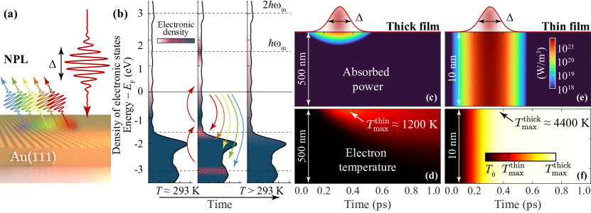
Upon optical excitation, electrons in the metal partially absorb the pump energy, thus being heated to high temperatures, which together with direct multiphoton optical transitions are responsible for the resulting PL, as observed in gold nanoparticles Biagioni et al. (2009); Roloff et al. (2017); Jollans et al. (2020) (see Fig. 1b). In gold films, we assume that the pump beam is laterally wide enough to consider the problem to be one-dimensional, such that we only need to analyze the dependence on the coordinate along the out-of-plane direction. We simulate the depth and time dependence of the electron temperature produced by a 150 fs Gaussian pump pulse having a moderate fluence of mJ/cm2 and a central wavelength nm (i.e., eV) with the TTM given by Block et al. (2019); Chen et al. (2010); Zhang et al. (2015); Rethfeld et al. (2017)
| (1) |
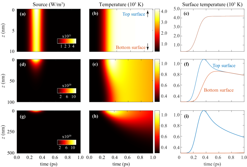
where is the heat capacity, is the electron thermal conductivity, is the electron-phonon coupling coefficient, is the temperature of the lattice, and is the absorbed power from the optical femtosecond pulse (see the details in the Appendix). We find the absorbed power to exhibit different characteristics for thick and thin films, as illustrated in Figs. 1c and 1e for 500 nm and 10 nm thickness, respectively. In the thicker film, the optical pump field only penetrates a few tens of nanometers (as determined by the skin depth, or equivalently, the light propagation length nm with ), while a peak electron temperature K is found at the top surface, partly attenuated by heat diffusion towards the bulk of the metal. In contrast, the same excitation in the thinner film, the excitation nearly uniformly permeates the entire metal volume because the thickness is no longer large compared with the skin depth, and optical surface reflections produce a more uniform field intensity. In addition, such reflections enhance the optical field in the metal, which together with the marginal role played by thermal diffusion, leads to a higher peak surface temperature K. The temperatures found in thin and thick films are both high enough to significantly affect the PL response because eV, so that electron-hole radiative recombination can occur with some probability by emitting photons of energy exceeding the pumping photon energy. This additional mechanism contributing to the PL at energies beyond the pump photons has an inelastic nature, in contrast to the few-transition processes associated with multiphoton absorption followed by radiative recombination (e.g., in TPP). As we shall see, these two mechanisms compete in importance depending on the thickness of the metal and the fluence of the pump.
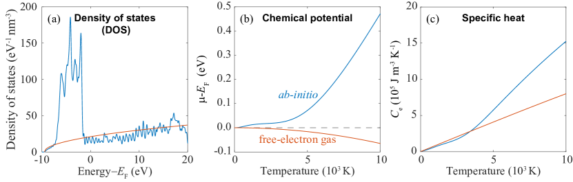
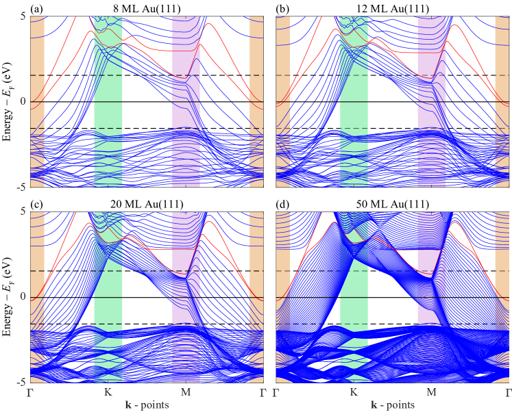
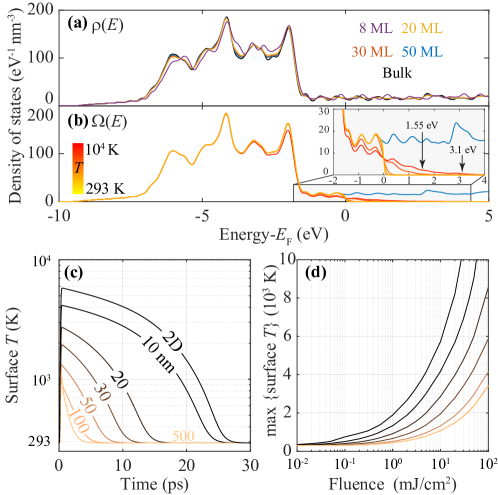
Interestingly, finite-size effects associated with the thickness start to be observed below nm, corresponding to gold atomic monolayers (MLs) with a (111) crystal orientation (considering an interlayer spacing of nm). To illustrate this effect, Fig. 2a shows the 2D electronic density of states (DOS) obtained for 8, 20, 30, and 50 MLs as well as for a semi-infinite surface. These results are computed from the band structure energies , summed over the band index and electron wave vector (see eq (7) in the Appendix). When approaching 50 MLs ( nm), the features in the DOS resemble those of the bulk, supporting the idea that band-structure phenomena become important only for few-atomic-thick films. Therefore, from the band structure viewpoint, gold films with thicknesses nm are considered to behave approximately equivalent to the bulk. However, for the thermal behavior of such films, as we have anticipated in Fig. 1, there exist large differences between 10 nm and 500 nm thick films regarding the temporal evolution and fluence dependence of the electron temperature. Importantly, note that we connect the TTM with the band structure of the film by computing the temperature-dependent chemical potential from the DOS, and also the heat capacity that enters in the TTM analysis, see the Appendix and Fig. 7 in Supplementary Figures.
The electronic bands are populated according to the Fermi–Dirac (FD) statistics, given by the electron energy and temperature as
| (2) |
We also define the occupation density , which varies accordingly with temperature (see Fig. 2b), such that a larger number of bands become populated at higher temperatures. Due to heating produced by optical absorption from the pump, the PL signal is dominated by electron dynamics near the surface, which is precisely where the temperature reaches its larger values. As shown in Fig. 2c, the surface electron temperature increases rapidly once the pulse hits the surface (see Fig. S2 in SI). We observe two main effects: (1) thinner films reach higher temperatures compared with semi-infinite films; and (2) thinner films retain the temperature much longer than their bulkier counterparts. Thinner films boost the electric field intensities due to multiple reflections of the pump field inside the film (similar to a Fabry–Pérot resonator), causing them to absorb a larger fraction of the pump energy and thus reach higher temperatures. Additionally, the fact that they are thinner reduces the influence of thermal diffusion in the TTM, hence removing such a cooling mechanism, which is in contrast significant for thicker films. The diminished role of the diffusion term implies that for thinner films the influence of the source is effectively instantaneous, and in the extreme case of a few atomic layers, diffusion (driven by the temperature gradient) can be ignored, giving rise to what we name 2D limit. Therefore, the range of surface temperatures varies from the 2D limit to the bulk limit, as illustrated in Fig. 2d. Films with an intermediate thickness (e.g., between 50 nm and 200 nm) present a hybrid behavior in which the temperature requires hundreds of nanoseconds to reach thermal equilibrium across the film thickness (see Fig. 2 in the SI).
The PL emission intensity is proportional to the number of photons that undergo transitions from excited states to lower-energy states by emitting a photon with energy . The spectral profile of the PL is thus given by
| (3) |
where the sum extends over the contributions of nearly vertical transitions (i.e., the photon energy is negligible compared to the size of the Brillouin zone) for each -point in the electronic band structure and
| (4) |
is defined in terms of the radiative decay rate (from band to band at a given point), the occupation factor of the electronic state with energy , the linewidth of the final state (see eq (8)), and the Heaviside distribution with argument . The electronic population evolves with time according to the rate equation Saavedra et al. (2016)
| (5) | ||||
where is a phenomenological damping rate, is the thermalized population, and is the excitation composed of the linear absorption and to the fourth power, establishing the rule characteristic of the TPP (see the details in the Appendix). Note that all quantities depend on temperature, which evolves in time following the TTM given in eq (1).
II.1 Thickness dependence of nonlinear photoluminescence
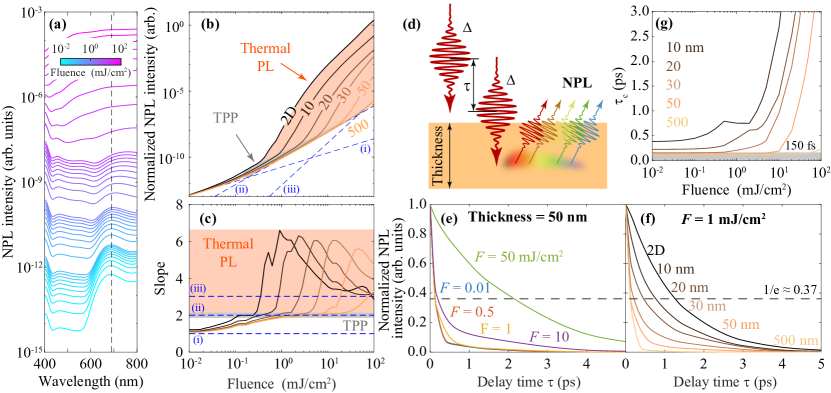
In Fig. 3a, we plot the NPL spectral emission profile for a gold film of 50 nm thickness calculated from eq (3) for a set of fluences indicated in the legend (within a range spanning four orders of magnitude) using a pulse width fs. We observe that, in this particular case, the resulting PL spectrum is peaked at nm. When increasing the temperature, the emission peaks fade away to yield a broader spectrum.
To analyze the dependence of the NPL signal on thickness, we define the normalized intensity as
| (6) |
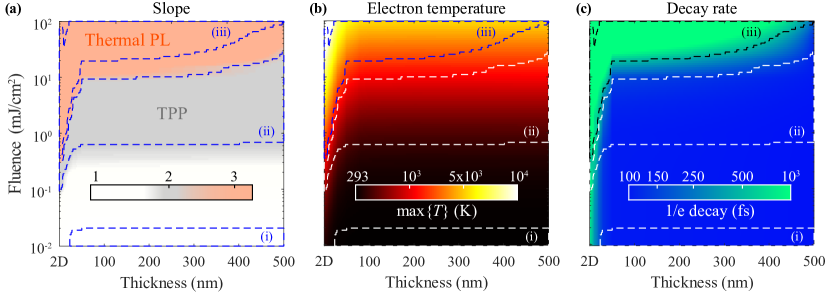
where the integration area covers the spectral region between the second-harmonic frequency and the fundamental frequency . We compute the normalized intensity as a function of fluence in Fig. 3b for various values of film thickness, which clearly shows how the PL signal produced by thinner films reaches much higher values than that of thicker ones. For fluences mJ/cm2, the PL signal displays a linear dependence on pulse fluence, indicating that nonlinear absorption processes are not large enough to dominate the electronic response. However, for fluences between mJ/cm2 and mJ/cm2, the dependence for semi-infinite films is dominated by two-photon absorption following the rule and, therefore, being responsible for the TPP (i.e., a scaling with fluence). Incidentally, for any fluence within the mJ/cm2 range, the PL emission grows with decreasing film thickness faster than the square of the fluence, suggesting that thermal effects dominate. The gray shaded area highlights the region (denoted TPP) in which two-photon absorption dominates, whilst the orange area corresponds to dominance of thermal effects (denoted thermal PL). These regions are limited by the bulk (effectively investigated for a 500 nm thick film) and 2D-thin film limits. We observe a gradual change in the PL intensity when the film thickness varies from 50 nm to 10 nm. The actual transition through the different regimes (NPL and thermal PL) might vary with the excitation wavelength , which is directly associated with the optical penetration depth in which optical absorption takes place.
We identify the region in which the rule governs the emission by taking the derivative of the normalized intensity with respect to the incident fluence to compute its slope (see Fig. 3c). As a guide, we show blue dashed lines with slopes of 1, 2, and 3, respectively labeled (i), (ii), and (iii) in the figure. Within the grey shaded area, TPP dominates the NPL emission, which is overtaken by thermal PL when the electron temperature is elevated above a few thousands of degrees. We observe the transition from the TPP to thermal PL in Fig. 9a in Supplementary Figures, representing a fluence-thickness phase diagram, in which the same blue dashed curves corresponding to slopes of 1–3 are used to limit different regions. Additionally, Fig. 9b in Supplementary Figures shows a phase diagram of the maximum surface electron temperature, corroborating that thermal effects become relevant at temperatures larger than K.
II.2 Two-pulse correlation in nonlinear photoluminescence
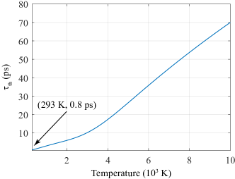
As concluded above, the resulting NPL emission in gold films is driven by both TPP and thermal PL, depending on the pump fluence and film thickness. Each of these two mechanisms has its characteristic time scale, which can be interrogated by two-pulse excitation: we can study the NPL emission intensity when a copy of the pulse impinges on the sample at a time after the original one (see the sketch in Fig. 3d). Two-pulse correlation analysis is a powerful tool for studying the temporal electron dynamics, introducing a new parameter (i.e., the delay between the two copies of the pulse) besides the pulse intensity. The two pulses interact optically within a time window limited to the pulse width (i.e., fs in our study), whereas the characteristic time for thermal effects is given by according to eq (1). The latter spans a range from ps to ps for electron temperatures from K to K (see values of in Fig. 10 in Supplementary Figures).
The normalized intensity changes as shown in Fig. 3e for different values of the fluence in a film of 50 nm thickness. For such a film thickness, fluences below 10 mJ/cm2 drive TPP, corresponding to values of 1/e decay below the picosecond (see Fig. 3g). However, for larger fluences (see green curve in Fig. 3e), the decay rate of the two-pulse correlation curve increases considerably to several picoseconds. Conversely, thermal effects dominate the PL signal at low fluences in thinner films, as shown in Fig. 3f for mJ/cm2 and several values of the film thickness. Corroborating this assignment, when thermal effects dominate the response, the decay rate is of the order of picoseconds and increases with increasing surface electronic temperature (i.e., for thinner films). In contrast, in the NPL regime, the decay rate is of the order of hundreds of femtoseconds and does not show significant dependence on fluence or temperature.
These results are in agreement with those discussed above for single pulses, in connection to Fig. 3b-c, and consistent with the fact that thinner films reach higher surface electron temperatures under the same fluence, and therefore, the NPL emission for thinner films extends over a longer time scale of the order of picoseconds. As a summary, we plot in Fig. 3g the characteristic decay time as a function of fluence for various film thicknesses, showing that the width is of the order of hundreds of femtoseconds at fluences below a threshold value, characteristic of the given film thickness.
II.3 Band structure effects in nonlinear photoluminescence
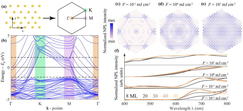
The emitted NPL corresponds to the collective emission of electrons from excited to lower energy states (see eq (4)). The electron energy levels are given in terms of in-plane crystal momentum from the computed band structure, which is sensitive to the crystallographic arrangement of atoms in the film. Figure 4a depicts the arrangement of atoms in a (111) crystallographic orientation and the associated Brillouin zone in 2D reciprocal space, where we identify the high-symmetry points , M, and K. The band structure traversing these high-symmetry points is obtained from ab-initio calculations of a 10 ML Au(111) film and presented in Fig. 4b for energies relative to the Fermi energy . Interestingly, the PL from each of these points in the band structure directly depends on the strength of the dipole transition matrix element (see Appendix) between the involved states. In Fig. 4c-e we present the intensity of the emitted NPL for several fluences at the discretized points of the Brillouin zone to emphasize that there are preferable areas of emission in the reciprocal space. For low values of the fluence (panel (c)), and therefore, in the TPP regime, most of the emission correlates with the and M points. Additionally, there is a contribution from the K connection that correlates with the region in the band structure diagram in Fig. 4b, where the electronic bands cross the Fermi energy, in concordance with previous works Boyd et al. (1986); Imura et al. (2004, 2005); Bouhelier et al. (2005). These features become more intense when the fluence is larger, as observed in panel (d), which would correspond to a transient regime between the TPP and the thermal PL. Finally, in panel (e) when the regime clearly enters in the thermal PL, all the points in the band structure contribute to smear out any resolvable features.
Specific features in the electronic band structure that influence NPL depend on the crystal orientation of the material and on the number of atomic planes that compose the thin film. The energy levels and transition dipole matrix elements vary from the quasi-two-dimensional limit of a few MLs to the bulk regime (see Fig. 11 in Supplementary Figures), and consequently, the resulting NPL changes accordingly. In Fig. 4f, we plot the normalized NPL intensity for a set of fluences ranging four orders of magnitude and thus spanning the TPP and thermal PL regimes in few-atom-thick films. In the low-intensity regime, there is a well-defined peak at nm with an initially thickness-dependent amplitude that converges to a bulk value for a larger number of MLs. As observed in Fig. 4c–e, the distinguishable features in reciprocal space fade with increasing pulse fluence, so that a broad range of transitions spanning a larger bandwidth of emission wavelengths can contribute to the overall NPL. Such behavior is reminiscent of blackbody radiation. Besides the general trend regarding the intensity of the impinging electric field, there are spectral differences depending on the number of MLs, which correlate with the band structure and are stronger in the TPP regime.
II.4 Experimental inside and theory-experiment comparison
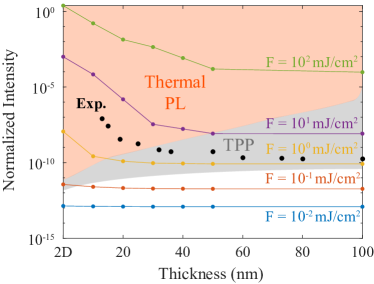
Before analyzing our measurements for crystalline gold flakes, we compare the above theory with the experiments in ref 12, which reports NPL emission from (111) surfaces of monocrystalline gold films with varying thickness. The results are shown in Fig. 5, where we plot the thickness dependence of the NPL signal as a function of film thickness for various values of the pump fluence. The superimposed experimental data, normalized to the theory values for a 100 nm thick film, matches reasonably well with our theory. Furthermore, the transition from the TPP to the thermal PL regime as thickness decreases corresponds to the threshold for which a deviation from the rule is observed in experiment Großmann et al. (2019).
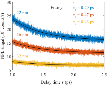
To obtain additional insight into the NPL dynamics, we perform two-pulse correlation experiments on a monocrystalline gold flake sample that has varying thickness (similar to the samples in ref 12). Further details about the sample preparation and optical characterization can be found in the Appendix. The measured two-pulse correlation traces of the NPL signal for gold thicknesses of approximately 22 nm, 26 nm, and 32 nm obtained at mJ/cm2 fluence are shown in Fig. 6. For the fitting, we consider only the signal obtained for delay times significantly larger than the pulse length ( ps) to avoid capturing any optical interaction effects (full measurement range correlation curves, including the pulse interference, are provided in Fig. 12f in Supplementary Figures). The fitting of transient signals in Fig. 6 reveals that the characteristic decay time increases for smaller thickness (from ps to ps). These extracted decay times are comparable to those found in previously reported measurements on thick polycrystalline gold films Wang et al. (1994), although they are smaller by approximately a factor of 2 in comparison with prior time-resolved NPL measurements on nanostructured gold Jiang et al. (2013); Biagioni et al. (2012); Bauer et al. (2015); Sakat et al. (2016); Mejard et al. (2016); Xie et al. (2019), in which the reported values are of the order of ps. Such a discrepancy can be explained by the field enhancement associated with localized surface-plasmon resonances in measurements involving nanostructures or nanoantennas, which give rise to higher electronic temperatures that bring the PL signal to the thermal regime for smaller fluences than for the thin films. In the aforementioned references, the measured decay times are interpreted as the lifetimes of electron-hole pair excitations in the three-step model (i.e., an intermediate state in a cascaded absorption process). According to our model, the observed decay in two-pulse NPL correlation mainly stems from the thermal PL effects provided that the optical interaction time is much smaller (i.e., ). However, for the experimentally investigated range of thicknesses and fluence, our model predicts longer characteristic decay time (see Fig. 3g), being in a seemingly better accordance with the values reported for nanostructured metals. However, the gold flake sample has a larger lateral dimension ( m) and the excitation spot area is limited to roughly 1 m2. This suggests that a lateral diffusion mechanism might take place in the direction parallel to the film surface and, therefore, effectively reduce as compared to metal nanostructures with dimensions smaller than the excitation spot. Consequently, the experimentally measured decay time can be interpreted as a result of the interplay between the thermal ( ps) and lateral diffusion ( ps) effects, which have comparable (and thus hardly distinguishable) characteristic decay times, as shown in the Appendix.
III CONCLUSIONS
We reveal the pivotal role played by electronic thermal effects in the nonlinear optical response (specifically, the nonlinear photoluminescence) of thin metal films depending on thickness and light intensity. We support this conclusion with a theoretical formalism incorporating first-principles details of the electronic band structure, in excellent agreement with available experiments, including our nonlinear photoluminescence measurements for crystalline gold films of 10–100’s nm thickness.
When the film thickness decreases, the electron temperature at the surface during optical pumping increases considerably, by up to thousands of degrees, making thermal effects dominant under the right combination of incident fluence and thickness. However, thick films are capable of quickly diffusing the absorbed heat into the bulk, thus reducing the influence of thermal effects. Therefore, in the thick-film regime and under relatively low pump intensities (fluences of the order of 50 mJ/cm2), we conclude that thermal effects are negligible, and TPP dominates the NPL emission with a well-defined fourth power dependence on the amplitude of the incident electric field ( rule, or equivalently, the square of the fluence). In contrast, thinner films absorb larger power densities, yielding higher peak temperatures at the surface (i.e., the regions that produce the bulk of the NPL emission, essentially limited to the skin depth) for longer times, and therefore making thermal PL a dominant mechanism that is characterized by an efficiency larger than the rule characteristic of TPP.
Additionally, the TPP and thermal PL mechanisms exhibit distinct characteristic times that we have interrogated by simulating two-pulse correlation of TPP. Exploring the effect of thickness and fluence in the TPP region, the dynamics associated with two-pulse illumination is controlled by the pulse duration, which in this case is of the order of 150 fs, whereas for thermal PL the characteristic times are found to be of the order of picoseconds, in agreement with available experiments. Our explanation of such experiments is thus introducing thermal PL as a new ingredient whose importance has been previously overlooked. Additionally, lateral thermal diffusion becomes relevant for extended films, yielding smaller characteristic decay rates compared to finite systems such as nanoparticles, where diffusion is limited.
Further analysis is still required to understand NPL emission from few-atom-thick gold films. We expect that the changes associated with spatial confinement in the band structure will manifest in the TPP signal for metal films of thickness below 10 MLs ( nm), which is a regime accessible to state-of-the-art sample preparation Abd El-Fattah et al. (2019). We envision that the use of atomically thin films with crystalline surface quality will be crucial in the next generation of nanoscale photonic devices, and therefore, the understanding of their optical properties constitutes a current challenge demanding additional explorations in the line suggested by the present work.
ACKNOWLEDGEMENTS
We thank C. Wolff for stimulating discussions. This work has been supported in part by ERC (Advanced Grant 789104-eNANO), the Spanish MICINN (PID2020-112625-GB-I00 and Severo Ochoa CEX2019-000910-S), the Catalan CERCA Program, and Fundaciós Cellex and Mir-Puig. A.R.E. acknowledges support from the Generalitat de Catalunya, the European Social Fund (L’FSE inverteix en el teu futur)-FEDER. J.D.C. is a Sapere Aude research leader supported by Independent Research Fund Denmark (Grant No. 0165-00051B). N.A.M. is a VILLUM Investigator supported by VILLUM FONDEN (Grant No. 16498). The Center for Polariton-driven Light–Matter Interactions (POLIMA) is funded by the Danish National Research Foundation (Project No. DNRF165).
APPENDIX
Appendix A Electronic properties of metal films
We characterize the electronic structure of a film by calculating the one-electron energies as a function of wave vector within the Brillouin zone for each band index (see the details in below), from which we compute the DOS (see Fig. 7a in Supplementary Figures) according to
| (7) |
where is the unit-cell volume, denotes the weight of each point (here set to to account for spin degeneracy), and the function
| (8) |
introduces a phenomenological linewidth that we set to eV in order to avoid artefacts associated with the discretized -space. The density of occupied states is then defined as , where the FD distribution at temperature is computed from eq (2), which involves the chemical potential (see Fig. 7b in Supplementary Figures). Finite temperature effects are incorporated by computing self-consistently, imposing the conservation of electron density Ashcroft and Mermin (1976)
| (9) |
We also require the energy density
| (10) |
from which we obtain the specific heat (Fig. 7c in Supplementary Figures) as
| (11) |
Appendix B Thermo-optical response
We consider an extended thin metal film illuminated by a well-collimated ultrafast optical pulse impinging normal to the film along the direction, such that the electric field within the film can be approximately written as
| (12) |
where is the pulse carrier frequency, the function accounts for the spatial profile produced by scattering at the film surfaces, and
| (13) |
characterizes the temporal Gaussian envelope of the pulse, with a FWHM pulse duration satisfying the normalization condition . Incidentally, we introduce an offset of the pulse center such that the light intensity is negligible at . The power absorbed by the film is then given by
| (14) |
where is the bulk dielectric function of the metal and the peak intensity is specified in terms of the pulse fluence . For the two-pulse calculations, we superimpose a copy of the original pulse, delayed by a time , so that we make the substitution in eq (14).
Heating caused by optical pumping produces a raise in the electron temperature and the lattice temperature , which we describe with the TTM given in eq (1), in which is the electronic heat capacity from eq (11), is the electronic thermal conductivity in the linear-temperature-dependence regime, with W m-1K-1 for gold Bonn et al. (2000), and W m-3K-1 is the electron-lattice coupling coefficient Lee et al. (2011). Incidentally, we consider wide pump spots illuminating the samples, so for simplicity, we assume no dependence on lateral position. This assumption is exact for extended plane-wave illumination, but it should be a good approximation for large optical spots compared to the film thickness. Thus, the electron temperature is governed by the one-dimensional diffusion problem of eq (1), which is further simplified by assuming a constant lattice temperature K. This approximation provides a simplified description of the lattice electron cooling channel, and is justified for the pulse fluences considered in this work. The dependence of the electron temperature on distance to the surface and time is illustrated in Fig. 8 in Supplementary Figures for the types of pump pulses and thicknesses here considered as obtained by numerically solving eq (1).
The above calculation involves the optical field profile across the out-of-plane direction (see eq (12)). Such profile is obtained by accounting for refraction and transmission at the film surfaces at and as well as propagation inside the film of thickness . The metal is described by a dielectric function and the film is hosted in a homogeneous dielectric medium of permittivity . We approximate the profile by computing it at the central wavelength, such that the optical field consists of plane waves that propagate in the direction with wave vectors in the metal () and dielectric () media. We consider normally incident light, and therefore, the electric field is along an in-plane direction. Then, solving the electromagnetic boundary conditions, we find that the spatial profile of the electric field reads
| (15) |
where the film external reflection and transmission coefficients and , and their respective counterparts and within the film, are defined by
| (16a) | ||||||
| (16b) | ||||||
and expressed in terms of the single interface reflection and transmission coefficients and for . Here, the temperature-dependent dielectric function of the metal is assumed to be Block et al. (2019)
| (17) |
where the background polarizability accounts for screening of interband transitions, eV is the bulk plasma frequency Johnson and Christy (1972), and the phenomenological damping rate is comprised of temperature-dependent electron-electron and electron-phonon contributions that are defined as Lawrence (1976); Beach and Christy (1977); O’Reilly (2017)
| (18) |
in terms of scattering coefficients and . For gold, we take scattering parameters and Lawrence (1976), a Fermi energy eV Ashcroft and Mermin (1976), a Debye temperature K O’Reilly (2017) equivalent to meV, and an inelastic broadening eV, such that meV at room temperature, in agreement with measured optical data Johnson and Christy (1972).
Appendix C Electron temperature evolution in the thermalised regime
Thermal effects have a much longer time scale (of the order of picoseconds, as seen for in Fig. 10 in Supplementary Figures) than the optical pump region that extends up to fs after the peak, which corresponds to twice the pulse FWHM. Therefore, after the pump is gone, the temperature quickly thermalises across the film (see Fig. 8 in Supplementary Figures) and eq (1) for the TTM becomes
| (19) |
For temperatures K, the heat capacity depends linearly on the temperature as (see Fig. 7c in Supplementary Figures), in which case the solution of the above differential equation can be obtained analytically as
| (20) |
which, for short times when the temperature is similar to the initial temperature , leads to a linear time dependence . Such linear behavior can be appreciated in Fig. 8c,f,i in Supplementary Figures
Appendix D Lateral diffusion
In the case of thin films (thickness below nm), diffusion in the perpendicular direction to the surface occurs rapidly (see Fig. 8 in Supplementary Figures), and therefore, the diffusion equation considering a homogeneous excitation (e.g., excitation Gaussian beam) retaining lateral thermal flux terms yields
| (21) |
in cylindrical coordinates, where is the radial coordinate starting from the center of the excitation source. If we only consider the dispersion part (i.e., neglecting the coupling to the lattice term ), and assuming that we are in the linear regime of the heat capacity (see Fig. 7c in Supplementary Figures), the above equation is satisfied by
| (22) |
provided a spatially Gaussian distribution as an initial condition, which corresponds to a Gaussian that keeps the integrated area constant at any time. Interestingly, near the center of the Gaussian (i.e., ), the time for which its temperature drops from the initial value results in , which for a beam waist nm, Wm-1, and Jm-3K-2, give rise to ps.
Appendix E Electronic dynamics
The electronic distribution of the metal film is described by the occupation factors of band at wave vector , which are initially determined by the FD distribution of eq (2) at temperature (i.e., ). The time evolution of the electronic distribution during optical excitation and subsequent thermalization is described by the population rate equation given in eq (5). The electronic wave vector is assumed to be conserved in the transitions associated with light absorption or emission, as the photon momentum is negligible compared to the size of the Brillouin zone at the optical frequencies under consideration. Nevertheless, non-vertical transitions are phenomenologically incorporated through the thermal relaxation term in eq (5). The optical excitation is described through a rate , comprising a linear absorption component,
| (23) |
and a two-photon absorption part,
| (24) |
both expressed in terms of the linewidth of the final state given in eq (8), the field intensity , the temporal pulse profile in eq (13), the energy differences , and the electronic transition dipole matrix elements Boyd (2008), with in-plane coordinates . Note that the two contributions at frequencies in either optical excitation process account for absorption () and stimulated emission () that excite or de-excite electrons when the population difference is nonzero according to eq (5). Spontaneous emission acts only to de-excite electrons to lower energies at a rate
| (25) |
which is directly related to the Einstein -coefficient Saleh and Teich (2019).
Appendix F Density-functional theory (DFT) calculations
We obtain the one-electron band structure (e.g., see Fig. 11 in Supplementary Figures) and dipole transition matrix elements of thin gold films consisting of up to 50 MLs from density-functional theory (DFT) calculations using Quantum Espresso Giannozzi et al. (2009) combined with the Perdew–Burke–Ernzerhof (PBE) Perdew et al. (1996) parametrization of the generalized gradient approximation. We adopt optimized norm-conserving Vanderbilt Hamann (2013); Schlipf and Gygi (2015) pseudopotentials with a kinetic energy cut-off of 80 Ry. Energy minimization yields a bulk lattice constant of 4.155 Å, which we use to construct thin gold films by fixing the interatomic bond distances. A vacuum spacing of 10 Å is introduced in the vertical direction to avoid spurious interactions between neighboring cells. We use a 24241-grid to calculate electronic structures. Using the resulting Kohn–Sham wave functions and eigenvalues, we obtain the transition dipole matrix elements using the YAMBO code Marini et al. (2009).
Appendix G Experimental methods
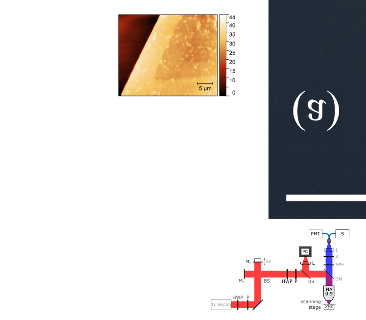
The gold flake sample was synthesized in an endothermic reduction of HAuCl4 precursor, following the prescription of refs 63 and 64. In short, 20 l of 0.5 M aqueous solution of HAuCl4 was mixed with 5 mm of ethylene glycole (both reagents from purchased from Sigma Aldrich) and vigorously stirred. Further, a pre-cleaned (ultrasonication in acetone, isopropyl alcohol and deionized water) glass cover slip (Menzel 1) was immersed in the solution and left on a hot plate at 100∘C. After 24 h, the glass cover slip is removed from the growth solution, rinsed with isopropyl alcohol and deionized water, and dried in a nitrogen flow. This procedure results in a large batch of gold flake samples with varying thicknesses. An optical image, atomic-force microscope topography and a NPL confocal map of the investigated flake sample are shown in Fig. 12a-c in Supplementary Figures.
Two-pulse correlation measurements were performed using an experimental setup based on a custom-made scanning nonlinear microscope (schematics of the setup are shown in Fig. 12g in Supplementary Figures). The laser source used in the experiment is a mode-locked titanium-sapphire (Ti:sapph) oscillator (Tsunami 3941 by Spectra-Physics), which provides approximately 120 ps pulses with central wavelength 800 nm. The delay between the pulses is controlled by moving a mirror in the delay arm of the Michelson interferometer setup, through which the laser beam goes before entering the microscope. In the two-pulse correlation measurements, we detect only the NPL content of the broad nonlinear signal (see spectral measurements in Fig. 12d in Supplementary Figures): the second-harmonic peak is filtered out using an appropriate band-pass filter. The measurements were performed in reflection mode, using a objective to focus the excitation light down to a diffraction-limited spot ( m diameter) and collect the nonlinear signal. To maximize the signal, we used approximately 10 mJ/cm2 fluence (averaged within the focal spot), which, according to our fluence dependence measurements (see Fig. 12e in Supplementary Figures) is still within the two-photon process range.
References
- Mooradian (1969) A Mooradian, “Photoluminescence of metals,” Phys. Rev. Lett. 22, 185 (1969).
- Farrer et al. (2005) Richard A. Farrer, Francis L. Butterfield, Vincent W. Chen, and John T. Fourkas, “Highly efficient multiphoton-absorption-induced luminescence from gold nanoparticles,” Nano Lett. 5, 1139–1142 (2005).
- Beversluis et al. (2003) Michael R Beversluis, Alexandre Bouhelier, and Lukas Novotny, “Continuum generation from single gold nanostructures through near-field mediated intraband transitions,” Phys. Rev. B 68, 115433 (2003).
- Imura et al. (2004) Kohei Imura, Tetsuhiko Nagahara, and Hiromi Okamoto, “Plasmon mode imaging of single gold nanorods,” J. Am. Chem. Soc. 126, 12730–12731 (2004).
- Yelin et al. (2003) Dvir Yelin, Dan Oron, Stephan Thiberge, Elisha Moses, and Yaron Silberberg, “Multiphoton plasmon-resonance microscopy,” Opt. Express 11, 1385–1391 (2003).
- Sheppard (2020) Colin JR Sheppard, “Multiphoton microscopy: a personal historical review, with some future predictions,” J. Biomed. Opt. 25, 014511 (2020).
- Petek and Ogawa (1997) H. Petek and S. Ogawa, “Femtosecond time-resolved two-photon photoemission studies of electron dynamics in metals,” Prog. Surf. Sci. 56, 239–310 (1997).
- Abd El-Fattah et al. (2019) Z. M. Abd El-Fattah, V. Mkhitaryan, J. Brede, L. Fernández, C. Li, Q. Guo, A. Ghosh, A. Rodríguez Echarri, D. Naveh, F. Xia, J. E. Ortega, and F. J. García de Abajo, “Plasmonics in atomically thin crystalline silver films,” ACS Nano 13, 7771–7779 (2019).
- Dryzek and Czapla (1987) J. Dryzek and A. Czapla, “Quantum size effect in optical spectra of thin metallic films,” Phys. Rev. Lett. 58, 721 (1987).
- Qian et al. (2015) Haoliang Qian, Yuzhe Xiao, Dominic Lepage, Li Chen, and Zhaowei Liu, “Quantum electrostatic model for optical properties of nanoscale gold films,” Nanophotonics 4, 413–418 (2015).
- Qian et al. (2016) Haoliang Qian, Yuzhe Xiao, and Zhaowei Liu, “Giant kerr response of ultrathin gold films from quantum size effect,” Nat. Commun. 7, 13153 (2016).
- Großmann et al. (2019) Swen Großmann, Daniel Friedrich, Michael Karolak, René Kullock, Enno Krauss, Monika Emmerling, Giorgio Sangiovanni, and Bert Hecht, “Nonclassical optical properties of mesoscopic gold,” Phys. Rev. Lett. 122, 246802 (2019).
- Chen et al. (1981) C.K. Chen, A.R.B. De Castro, and Y.R. Shen, “Surface-enhanced second-harmonic generation,” Phys. Rev. Lett. 46, 145 (1981).
- Hubert et al. (2007) Christophe Hubert, Laurent Billot, P.-M. Adam, Renaud Bachelot, Pascal Royer, Johan Grand, Denis Gindre, K. D. Dorkenoo, and Alain Fort, “Role of surface plasmon in second harmonic generation from gold nanorods,” Appl. Phys. Lett. 90, 181105 (2007).
- Slablab et al. (2012) A. Slablab, L. Le Xuan, M. Zielinski, Y. De Wilde, V. Jacques, D. Chauvat, and J.-F. Roch, “Second-harmonic generation from coupled plasmon modes in a single dimer of gold nanospheres,” Opt. Express 20, 220–227 (2012).
- Jiang et al. (2013) Xiao-Fang Jiang, Yanlin Pan, Cuifeng Jiang, Tingting Zhao, Peiyan Yuan, T. Venkatesan, and Qing-Hua Xu, “Excitation nature of two-photon photoluminescence of gold nanorods and coupled gold nanoparticles studied by two-pulse emission modulation spectroscopy,” J. Phys. Chem. Lett. 4, 1634–1638 (2013).
- Xie et al. (2019) Dan Xie, François O. Laforge, Ilya Grigorenko, and Herschel A. Rabitz, “Dual coherent and incoherent two-photon luminescence in single gold nanorods revealed by polarization and time-resolved nonlinear autocorrelation,” J. Opt. Soc. Am. B 36, 1931–1936 (2019).
- Boyd et al. (1986) G. T. Boyd, Z. H. Yu, and Y. R. Shen, “Photoinduced luminescence from the noble metals and its enhancement on roughened surfaces,” Phys. Rev. B 33, 7923 (1986).
- Imura et al. (2005) Kohei Imura, Tetsuhiko Nagahara, and Hiromi Okamoto, “Near-field two-photon-induced photoluminescence from single gold nanorods and imaging of plasmon modes,” J. Phys. Chem. B 109, 13214–13220 (2005).
- Bouhelier et al. (2005) Alexandre Bouhelier, Renaud Bachelot, Gilles Lerondel, Sergei Kostcheev, Pascal Royer, and G. P. Wiederrecht, “Surface plasmon characteristics of tunable photoluminescence in single gold nanorods,” Phys. Rev. Lett. 95, 267405 (2005).
- Sheik-Bahae and Hasselbeck (2000) Mansoor Sheik-Bahae and Michael P. Hasselbeck, “Third-order optical nonlinearities,” in Optical Properties of Materials, Nonlinear Optics, Quantum Optics, Handbook of Optics, Vol. IV (McGraw-Hill Education, New York, 2000) Chap. 17.
- Biagioni et al. (2009) P. Biagioni, M. Celebrano, M. Savoini, G. Grancini, D. Brida, S. Mátéfi-Tempfli, M. Mátéfi-Tempfli, L. Duò, B. Hecht, G. Cerullo, and M. Finazzi, “Dependence of the two-photon photoluminescence yield of gold nanostructures on the laser pulse duration,” Phys. Rev. B 80, 045411 (2009).
- Boroviks et al. (2021) S. Boroviks, T. Yezekyan, R. Rodríguez Echarri, F. J. García de Abajo, J. D. Cox, S. I.. Bozhevolnyi, N. A. Mortensen, and C. Wolff, “Anisotropic second-harmonic generation from monocrystalline gold flakes,” Opt. Lett. 46, 833–836 (2021).
- Muehlschlegel et al. (2005) Peter Muehlschlegel, H.-J. Eisler, Olivier J. F. Martin, Bert Hecht, and D. W. Pohl, “Resonant optical antennas,” Science 308, 1607–1609 (2005).
- Buhmann et al. (2012) S. Y. Buhmann, D. T. Butcher, and S. Scheel, “Macroscopic quantum electrodynamics in nonlocal and nonreciprocal media,” New J. Phys. 14, 083034 (2012).
- Biagioni et al. (2012) Paolo Biagioni, Daniele Brida, Jer-Shing Huang, Johannes Kern, Lamberto Duò, Bert Hecht, Marco Finazzi, and Giulio Cerullo, “Dynamics of four-photon photoluminescence in gold nanoantennas,” Nano Lett. 12, 2941–2947 (2012).
- Bauer et al. (2015) M. Bauer, A. Marienfeld, and M. Aeschlimann, “Hot electron lifetimes in metals probed by time-resolved two-photon photoemission,” Prog. Surf. Sci. 90, 319–376 (2015).
- Saavedra et al. (2016) J. R. M. Saavedra, A. Asenjo-Garcia, and F. J. García de Abajo, “Hot-electron dynamics and thermalization in small metallic nanoparticles,” ACS Photonics 3, 1637–1646 (2016).
- Dubi and Sivan (2019) Yonatan Dubi and Yonatan Sivan, ““hot” electrons in metallic nanostructures—non-thermal carriers or heating?” Light Sci. Appl. 8, 89 (2019).
- Haug et al. (2015) Tobias Haug, Philippe Klemm, Sebastian Bange, and John M Lupton, “Hot-electron intraband luminescence from single hot spots in noble-metal nanoparticle films,” Phys. Rev. Lett. 115, 067403 (2015).
- Fowler (1931) Ralph H. Fowler, “The analysis of photoelectric sensitivity curves for clean metals at various temperatures,” Phys. Rev. 38, 45 (1931).
- DuBridge (1932) Lee A. DuBridge, “A further experimental test of fowler’s theory of photoelectric emission,” Phys. Rev. 39, 108 (1932).
- DuBridge (1933) Lee A. DuBridge, “Theory of the energy distribution of photoelectrons,” Phys. Rev. 43, 727 (1933).
- Zhou and Zhang (2020) Yang Zhou and Peng Zhang, “A quantum model for photoemission from metal surfaces and its comparison with the three-step model and fowler–dubridge model,” J. Appl. Phys. 127, 164903 (2020).
- Mejard et al. (2016) Regis Mejard, Anthonin Verdy, Marlene Petit, Alexandre Bouhelier, Benoit Cluzel, and Olivier Demichel, “Energy-resolved hot-carrier relaxation dynamics in monocrystalline plasmonic nanoantennas,” ACS Photonics 3, 1482–1488 (2016).
- Roloff et al. (2017) Lukas Roloff, Philippe Klemm, Imke Gronwald, Rupert Huber, John M Lupton, and Sebastian Bange, “Light emission from gold nanoparticles under ultrafast near-infrared excitation: Thermal radiation, inelastic light scattering, or multiphoton luminescence?” Nano Lett. 17, 7914–7919 (2017).
- Jollans et al. (2020) Thomas Jollans, Martín Caldarola, Yonatan Sivan, and Michel Orrit, “Effective electron temperature measurement using time-resolved anti-stokes photoluminescence,” J. Phys. Chem. A 124, 6968–6976 (2020).
- García de Abajo (2014) F. J. García de Abajo, “Graphene plasmonics: challenges and opportunities,” ACS Photonics 1, 135–152 (2014).
- Rodríguez Echarri et al. (2021) A. Rodríguez Echarri, J. D. Cox, F. Iyikanat, and F. J. García de Abajo, “Nonlinear plasmonic response in atomically thin metal films,” Nanophotonics 10, 4149–4159 (2021).
- Boltasseva and Shalaev (2019) Alexandra Boltasseva and Vladimir M. Shalaev, “Transdimensional photonics,” ACS Photonics 6, 1–3 (2019).
- Lee et al. (2014) Jongwon Lee, Mykhailo Tymchenko, Christos Argyropoulos, Pai-Yen Chen, Feng Lu, Frederic Demmerle, Gerhard Boehm, Markus-Christian Amann, Andrea Alú, and Mikhail A. Belkin, “Giant nonlinear response from plasmonic metasurfaces coupled to intersubband transitions,” Nature 511, 65–69 (2014).
- Kubo et al. (2005) A. Kubo, K. Onda, H. Petek, Z. Sun, Y. S. Jung, and H. K. Kim, “Femtosecond imaging of surface plasmon dynamics in a nanostructured silver film,” Nano Lett. 5, 1123–1127 (2005).
- Block et al. (2019) A. Block, M. Liebel, R. Yu, R. Spector, Y. Sivan, F. J. García de Abajo, and N. F. van Hulst, “Tracking ultrafast hot-electron diffusion in space and time by ultrafast thermomodulation microscopy,” Sci. Adv. 5, eaav8965 (2019).
- Chen et al. (2010) AM Chen, HF Xu, YF Jiang, LZ Sui, DJ Ding, H Liu, and MX Jin, “Modeling of femtosecond laser damage threshold on the two-layer metal films,” Appl. Surf. Sci. 257, 1678–1683 (2010).
- Zhang et al. (2015) Jinping Zhang, Yuping Chen, Mengning Hu, and Xianfeng Chen, “An improved three-dimensional two-temperature model for multi-pulse femtosecond laser ablation of aluminum,” J. Appl. Phys. 117, 063104 (2015).
- Rethfeld et al. (2017) Baerbel Rethfeld, Dmitriy S. Ivanov, Martin E. Garcia, and Sergei I. Anisimov, “Modelling ultrafast laser ablation,” J. Phys. D 50, 193001 (2017).
- Wang et al. (1994) X. Y. Wang, D. M. Riffe, Y.-S. Lee, and M. C. Downer, “Time-resolved electron-temperature measurement in a highly excited gold target using femtosecond thermionic emission,” Phys. Rev. B 50, 8016–8019 (1994).
- Sakat et al. (2016) Emilie Sakat, Ilaria Bargigia, Michele Celebrano, Andrea Cattoni, Stéphane Collin, Daniele Brida, Marco Finazzi, Cosimo D’ Andrea, and Paolo Biagioni, “Time-resolved photoluminescence in gold nanoantennas,” ACS Photonics 3, 1489–1493 (2016).
- Ashcroft and Mermin (1976) N. W. Ashcroft and N. D. Mermin, Solid State Physics (Harcourt College Publishers, Philadelphia, 1976).
- Bonn et al. (2000) Mischa Bonn, Daniel N. Denzler, Stephan Funk, Martin Wolf, S.-Svante Wellershoff, and Julius Hohlfeld, “Ultrafast electron dynamics at metal surfaces: Competition between electron-phonon coupling and hot-electron transport,” Phys. Rev. B 61, 1101 (2000).
- Lee et al. (2011) Jae Bin Lee, Kwangu Kang, and Seong Hyuk Lee, “Comparison of theoretical models of electron-phonon coupling in thin gold films irradiated by femtosecond pulse lasers,” Mater. Trans. 52, 547–553 (2011).
- Johnson and Christy (1972) P. B. Johnson and R. W. Christy, “Optical constants of the noble metals,” Phys. Rev. B 6, 4370–4379 (1972).
- Lawrence (1976) W. E. Lawrence, “Electron-electron scattering in the low-temperature resistivity of the noble metals,” Phys. Rev. B 13, 5316–5319 (1976).
- Beach and Christy (1977) R. T. Beach and R. W. Christy, “Electron-electron scattering in the intraband optical conductivity of Cu, Ag, and Au,” Phys. Rev. B 16, 5277–5284 (1977).
- O’Reilly (2017) E. P. O’Reilly, Quantum theory of solids (Taylor & Francis, New York, 2017).
- Boyd (2008) Robert W. Boyd, Nonlinear Optics, 3rd ed. (Academic Press, Amsterdam, 2008).
- Saleh and Teich (2019) Bahaa EA Saleh and Malvin Carl Teich, Fundamentals of photonics (John Wiley & Sons, New York, 2019).
- Giannozzi et al. (2009) Paolo Giannozzi, Stefano Baroni, Nicola Bonini, Matteo Calandra, Roberto Car, Carlo Cavazzoni, Davide Ceresoli, Guido L. Chiarotti, Matteo Cococcioni, Ismaila Dabo, Andrea Dal Corso, Stefano de Gironcoli, Stefano Fabris, Guido Fratesi, Ralph Gebauer, Uwe Gerstmann, Christos Gougoussis, Anton Kokalj, Michele Lazzeri, Layla Martin-Samos, Nicola Marzari, Francesco Mauri, Riccardo Mazzarello, Stefano Paolini, Alfredo Pasquarello, Lorenzo Paulatto, Carlo Sbraccia, Sandro Scandolo, Gabriele Sclauzero, Ari P. Seitsonen, Alexander Smogunov, Paolo Umari, and Renata M. Wentzcovitch, “QUANTUM ESPRESSO: a modular and open-source software project for quantum simulations of materials,” J. Phys. Condens. Matter 21, 395502 (2009).
- Perdew et al. (1996) John P. Perdew, Kieron Burke, and Matthias Ernzerhof, “Generalized gradient approximation made simple,” Phys. Rev. Lett. 77, 3865–3868 (1996).
- Hamann (2013) D. R. Hamann, “Optimized norm-conserving vanderbilt pseudopotentials,” Phys. Rev. B 88, 085117 (2013).
- Schlipf and Gygi (2015) Martin Schlipf and François Gygi, “Optimization algorithm for the generation of ONCV pseudopotentials,” Comput. Phys. Commun. 196, 36–44 (2015).
- Marini et al. (2009) A. Marini, C. Hogan, M. Grüning, and D. Varsano, “Yambo: an ab initio tool for excited state calculations,” Comput. Phys. Commun. 180, 1392–1403 (2009).
- Krauss et al. (2018) Enno Krauss, René Kullock, Xiaofei Wu, Peter Geisler, Nils Lundt, Martin Kamp, and Bert Hecht, “Controlled growth of high-aspect-ratio single-crystalline gold platelets,” Cryst. Growth Des. 18, 1297–1302 (2018).
- Kiani and Tagliabue (2022) Fatemeh Kiani and Giulia Tagliabue, “High aspect ratio Au microflakes via gap-assisted synthesis,” Chem. Mater. 34, 1278–1288 (2022).
Appendix H SUPPLEMENTARY FIGURES