Control over epitaxy and the role of the InAs/Al interface in hybrid two-dimensional electron gas systems
Abstract
In-situ synthesised semiconductor/superconductor hybrid structures became an important material platform in condensed matter physics. Their development enabled a plethora of novel quantum transport experiments with focus on Andreev and Majorana physics. The combination of InAs and Al has become the workhorse material and has been successfully implemented in the form of one-dimensional structures and two-dimensional electron gases. In contrast to the well-developed semiconductor parts of the hybrid materials, the direct effect of the crystal nanotexture of Al films on the electron transport still remains unclear. This is mainly due to the complex epitaxial relation between Al and the semiconductor. We present a study of Al films on shallow InAs two-dimensional electron gas systems grown by molecular beam epitaxy, with focus on control of the Al crystal structure. We identify the dominant grain types present in our Al films and show that the formation of grain boundaries can be significantly reduced by controlled roughening of the epitaxial interface. Finally, we demonstrate that the implemented roughening does not negatively impact either the electron mobility of the two-dimensional electron gas or the basic superconducting properties of the proximitized system.
I Introduction
Material systems that combine semiconductors (SEs) and superconductors (SCs) have recently prompted novel research directions in condensed matter physics. The main motivation to study these systems are different approaches to quantum computing, e.g. Andreev Hays et al. (2021) and Transmon qubits Larsen et al. (2015); Casparis et al. (2018) or topological systems hosting Majorana bound states Sarma et al. (2015).
The combination of InAs and in-situ deposited Al has become an established material platform, either in the form of proximitized quasi one-dimensional hybrid nanowires or shallow two-dimensional electron gas (2DEG) systems Krogstrup et al. (2015); Shabani et al. (2016). The choice of InAs as the semiconducting part is due to its relatively high spin-orbit coupling and advantageous band alignment at the shallow SE/SC interface Mikkelsen et al. (2018). Furthermore, it exhibits good etching selectivity and chemical stability in device fabrication processes. The choice of Al is motivated by the possibility to achieve a high degree of epitaxial order on InAs Krogstrup et al. (2015), as well as by the fact that Al and InAs are mutually compatible with in-situ deposition in typical III-V Molecular Beam Epitaxy (MBE) systems, which often contain both the In and Al sources.
It was shown that the crystal structure of epitaxial Al films differs, depending on the implemented SE system. Krogstrup, et al. have shown in Ref. Krogstrup et al. (2015) that in-situ Al deposition on specific nanowire facets results in the formation of a single crystal Al film with thicknesses down to a few nanometers. Improving the interface between the materials resulted in a break-through, where a so-called "hard" superconducting gap was induced into the hybrid system, meaning that no sub-gap states were observed in tunneling spectroscopy measurements. This is in contrast to materials with ex-situ deposited Al, where sup-gap states are typically present Chang et al. (2015).
Nanowire-based systems have shown great promise as a platform for investigating transport phenomena Mourik et al. (2012); Vaitiekėnas et al. (2020); Kurtossy et al. (2021), however the lack of reliable schemes for scaling up to large device arrays limits their perspective for industrial applications. To address the scaling issue, growth of larger scale nanowire networks via selective area growth was recently developed Friedl et al. (2018); Krizek et al. (2018). Yet, the complementary 2DEG systems show more promise for large-scale applications, due to their compatibility with top-down fabrication techniques Aghaee et al. (2022).
In comparison to nanowires, the 2D systems reduce the spatial degrees of freedom for relaxation of the Al layer. This promotes the formation and co-existence of Al grains with various orientations after in-situ Al deposition, as previously reported in literature Sarney et al. (2018, 2020); Wang et al. (2020). Such grains in the Al film determine the local epitaxial relations to the underlying SE crystal and induce sharp grain boundaries into the system. There are strong indications that the formation of grain boundaries has a significant effect on the properties of superconducting thin films. For example, it was shown that the superconducting properties (e.g. critical temperature and critical magnetic field) of thin Al films can significantly exceed typical bulk values Ferguson et al. (2007), where extreme cases are found in granular aluminum films consisting of nano-sized Al grains Pracht et al. (2016). A different study has shown that the presence of grain boundaries modifies the oxidation dynamics of Al films Nguyen et al. (2018), which can cause oxidation beyond the thickness of native oxide (around 3 nm). This effect is not restricted to thin Al layers only, as the presence of grain boundaries in combination with strain have reportedly altered the SC properties of Nb thin films David Henry et al. (2014). Despite the presence of grain boundaries, a hard superconducting gap was also reported for Al in-situ deposited on shallow InAs 2DEG structures Kjærgaard et al. (2016).
In terms of hybrid materials, the direct effect of these local crystallographic changes in thin Al remains vastly unexplored, but recent studies have suggested that local disorder in superconducting films could play a key role in the functionality of superconducting qubits Richardson et al. (2016); de Leon et al. (2021) and proximitized SE/SC structures Cole et al. (2016); Thomas et al. (2022). Therefore, the nanotexturing of the Al thin films should be investigated in more detail, with particular emphasis on the growth of grain-free materials.
The direct way to improve the crystalline quality of the Al is to control the Al orientation on top of the SE 2DEG. This can be done either by the modification of the surface chemistry by capping the SE surface with different materials, where Sb-based interlayers have shown most promising results in promoting the growth of single crystalline Al films in recent studies Sarney et al. (2018, 2020). A disadvantage in this case is that presence of Sb often causes problems with the stability of the interface and device fabrication Thomas et al. (2019); Moehle et al. (2021). Another approach is to control the orientation of the Al by modifying the lattice constant of the underlying SE Wang et al. (2020). In that case, the engineered modification of the lattice constant within the quantum well region is necessarily related to a change in the electronic properties of the 2DEG, which may affect the desired balance between electron mobility and proximitized superconductivity.
Here, we introduce a novel approach to control thin Al film crystallinity. First, we give a detailed description of the growth of shallow InAs 2DEGs and analyse the strain evolution in the structure. This allows us to identify the most abundant defects responsible for relaxation within the metamorphic buffer layer and show that the lateral lattice spacing remains stable within the QW region of the 2DEG. Next, we identify the two dominant grain orientations responsible for grain boundaries in our in-situ grown epitaxial Al films. Furthermore, we demonstrate that controlled roughening of the SE surface can be implemented to grow grain-boundary-free Al films over scales of at least 5m. Finally, we find that the roughening does not negatively affect the mobility and electron density in the 2DEG, while preserving the functionality of the material in hybrid Josephson junctions (JJs).
II Growth of the semiconductor
The epitaxial Al films, which are the main focus of this work, were deposited on shallow InAs-based 2DEG structures Shabani et al. (2016). The InAs QWs were grown on semi-insulating Fe-doped (001) InP substrates by MBE. The native oxide of InP was desorbed at 530∘C for 3 minutes (growth temperature was measured by optical monitoring of the InP band edge Weilmeier et al. (1991)). The first lattice-matched 100 nm thick layer (x = 0.52) was grown at 510∘C, with a V/III ratio of 3.5 and at 1 Å/s. For the purpose of this work, the V/III ratio corresponds to the ratio of As4 and group III growth rate (details given in Methods sup ).
The lattice mismatch between the InP and InAs was compensated by growth of a step-graded metamorphic InxAl1-xAs buffer layer. The buffer consists of 20 steps with thicknesses of 50 nm, where x increases from 0.52 to 0.89 and was grown at 460∘C. We found the lowest semiconductor surface roughness for samples where the growth rate was increased from 1 to 1.5 Å/s and the V/III ratio was reduced from 2.3 to 1.8 when reaching x = 0.705. After the metamorphic buffer, a step-back step with x = 0.82 and a thickness of 8 nm was grown while maintaining the other growth conditions.
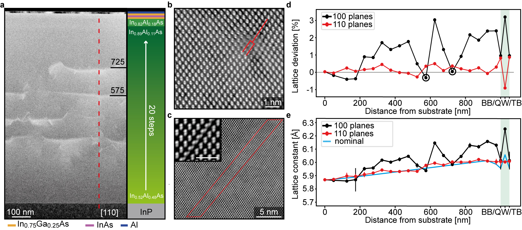
To further smoothen the surface before growth of the QW, a 50 nm thick virtual substrate was grown at 480∘C, using growth rate of 1.5 Å/s and V/III ratio of 3. The QW region consists of a 6.3 nm thick bottom In0.75Ga0.25As barrier, grown with V/III ratio of 2.75 while maintaining the growth rate of 1.5 Å/s and growth temperature of 480∘C. The 8.5 nm thick QW is grown at 1.125 Å/s and V/III ratio of 3.25. The In0.75Ga0.25As top barrier was grown under the same conditions as the bottom barrier. The full structure is illustrated and shown in the Annular Dark Field (ADF) Scanning Transmission Electron Microscope (STEM) image in Fig. 1a.
For the purpose of this study, we fixed the top barrier thickness to 13.4 nm, as this material configuration provided us with a good ratio of as-grown mobility and strength of the induced proximity effect, as discussed below. In our standard samples, the surface is capped with 2 mono-layers (MLs) of GaAs (at 0.375 Å/s), which provide a barrier for In diffusion into the Al film and improve chemical stability during device fabrication.
Adjustment of the growth conditions of the metamorphic buffer layer typically results in semiconductor surface without pronounced cross-hatching, isotropic cross-hatching or anisotropic cross-hatching, as shown in the Supplemental Material sup . For the optimized samples with strongly anisotropic cross-hatching, grown as described above, we measured electron mobilities around 50 000 cm2/(Vs) at electron densities around 41011 cm-2 at 4.2 K (measured in van der Pauw configuration on a 5x5 mm2 sample).
The structure of the SE is partially adapted from Ref. Shabani et al. (2016). In our case, we grew a thicker bottom barrier, upper barrier and QW. Yet, the SE/SC coupling in such a structure remained on a scale relevant for our transport experiments Haxell et al. (2022a, b); Hinderling et al. (2022); sup . We observed that the behaviour of our proximitized devices exceeds the theoretical limits given for specific barrier thicknesses in Ref. Shabani et al. (2016). This should be thoroughly investigated in future works, as the proximity effect in hybrid materials is expected to be affected by the interplay of strain, material composition of the barrier, QW dimensions, quality of the Al film and the epitaxial interface.
One of the important aspects of the SE structure is strain, which can strongly affect its transport properties, but also the epitaxial relation to the Al film. Strain fields related to defect formation and lattice relaxation in the InxAl1-xAs metamorphic buffer are clearly visible in the ADF STEM image in Fig. 1a. Importantly, they do not extend into the QW region, which remains defect free. The most abundant defects which dominate the relaxation and generate the strain fields are shown in High Angle Annular Dark Field (HAADF) STEM images in Fig. 1b and c. The first type, shown in b, are isolated misfit dislocations. The second type are single twin planes extending over tenths of nanometers, shown in c. Both defect types are randomly distributed throughout the strain relaxation region.
To further understand the strain distribution within the structure, we extracted the lateral and vertical lattice constants from STEM images by measuring the (10) and (001) lattice plane spacings (details are given in the Supplemental Material sup ) in the center of each layer along the red dashed line in Fig 1a. A percentual deviation from the bulk lattice constant is plotted as a function of distance from the substrate in Fig. 1d. As expected, the (110) lattice spacing is rather stable, while the (001) spacing expands and varies throughout the buffer layer. The (001) spacing shows two local minima, which overlap with the most strained regions visible in Fig. 1a. The measured lattice spacing is shown in Fig. 1d, showing that the lateral (110) lattice spacing remains almost constant in the QW region, as expected for growth on a relaxed virtual substrate. The average spacing and deviation is 6.00 0.02 Å for the bottom barrier, QW and top barrier, which yields 0.9 compressive strain compared to InAs. This negligible variation of the lattice constant is important, as the strain can be considered as fixed between the SE and Al. We observed a similar relaxation behaviour in multiple samples.
III Al thin films
For the in-situ Al deposition, the wafer was moved to an ultra-high vacuum buffer chamber (110-11 mbar) directly after growth of the shallow InAs 2DEG, and re-transferred when the pressure in the growth chamber reached 110-10 mbar, i.e., once the As background dropped after closing the As valve. The manipulator was rotated towards the liquid nitrogen shroud. No active cooling was involved and therefore the cooling power is only related to the MBE system being set to idle state and the sample holder going towards thermal equilibrium with LN2 cooled cryo-shrouds (in our system for at least 12 hours to reach approximately -30∘C). The Al films (12 nm thick in samples used in the presented transport experiments) were deposited at a rate of 1Å/s at a pressure of 3-510-11 mbar in the growth chamber. We note that the sample surface must remain cold during the deposition. Therefore, the used growth rate (controlled by the cell temperature) needs to be optimized for each specific MBE system geometry, as it determines heat delivered to the surface of the sample during growth. After the deposition, the wafer was moved to the load lock chamber (below 510-10 mbar). In order to prevent thermal dewetting of the Al film, we transferred the sample as fast as possible to the load lock, i.e., it remained cold until controlled oxidation. In our case, the sample was oxidized and brought to room temperature in the load lock by slowly venting with an Ar/O2 (90/10 %) mixture over the course of 15 minutes (at 25∘C). An AFM image of the oxidized surface for both the controlled oxidation and venting into atmosphere is shown in the Supplemental Material sup . The samples that were unloaded via controlled oxidation shown lower surface roughness and reduced formation of large AlOx grains than what we observed in samples directly unloaded into ambient atmosphere.
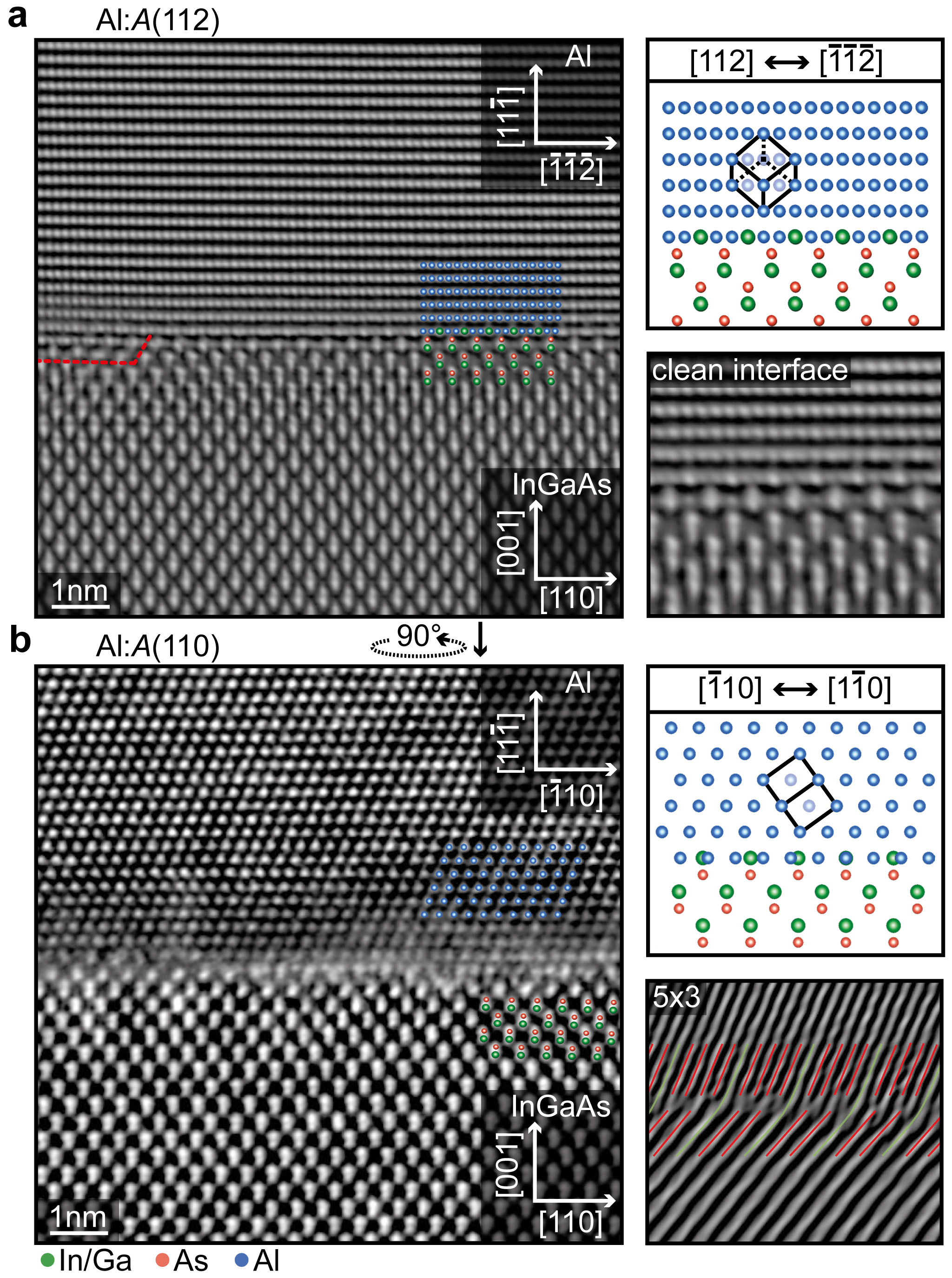
In our standard samples, where the surface was capped by depositing 2 MLs of GaAs and grown as described above, we mainly observe the presence of two distinctly oriented grains of Al. The first type is shown in Fig. 2. In this case, the Al with (111) out-of-plane orientation adapts either (112) in (a) or (110) in (b) lateral matching to the (110) planes of the semiconductor (here labeled as Al:(112) and Al:(110)). Therefore in STEM, it is possible to observe two distinct projections and epitaxial relations of the Al: crystal, depending on its alignment to the substrate. For the Al:(112) orientation shown in Fig. 2a, we observe a clean, fully epitaxial interface, with apparent (and ordered) intermixing within the first matching monolayers. For the Al:(110) orientation shown in Fig. 2b, we observe 5x3 matching, i.e., there are two misfit dislocations at the interface per 3 planes in the substrate.
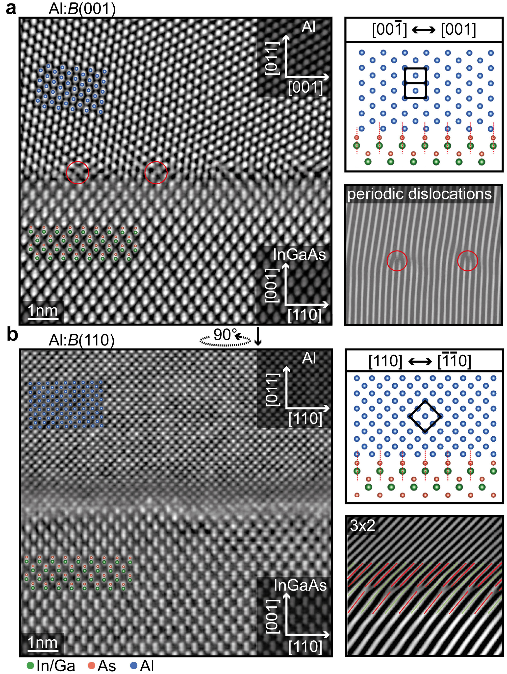
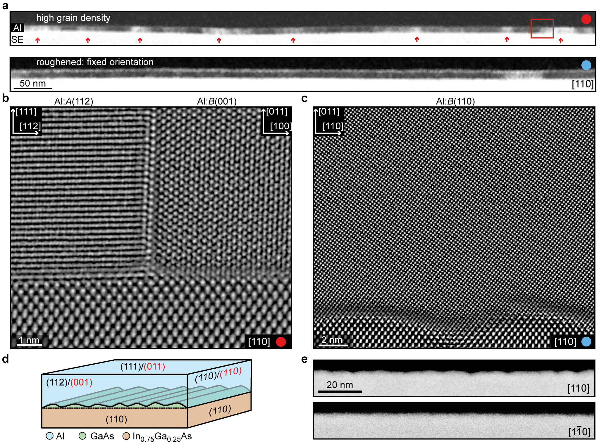
The second grain type is shown in Fig. 3, where the Al adapts (011) out-of-plane orientation and lateral matching as either (001) in (a) or (110) in (b) to the (110) planes of the semiconductor (here labeled as Al:(001) and Al:(110)). For this grain, we observe formation of misfit dislocations for both alignments to the (110) planes of the semiconductor. For the Al:(001) matching, the film relaxes by the formation of periodic arrays of misfit dislocations with larger spacing. In contrast, there is a single misfit dislocation per 2 planes in the substrate, i.e., a 3x2 match for the Al:(110) orientation. We observed that both grain types were equally present in the samples and often adapted small tilts (e.g. the slight tilt visible in Fig. 3a). A larger scale ADF-STEM overview of such a sample is shown in the top panel of Fig. 4a. The changing ADF contrast indicates a high density of grains with different orientation. The contrast can originate from the two different types of grains, mutual tilt of grains with the same orientation and/or from the two possible projections (i.e. 90∘ grain rotation). An example of a boundary between the two different grain types is shown in Fig. 4b. The smoothness of the SE surface in the HAADF STEM image indicates that the presence of the boundary is not associated with neither a surface step nor a crystallographic defect in the semiconductor.
These partially polycrystalline Al films performed consistently with previous reports in literature in our transport experiments which rely on the combined SE/SC system Haxell et al. (2022a, b); Hinderling et al. (2022); sup . On the other hand, consistent results were achieved only when processing temperatures did not exceed 175∘C. This is due to degradation of both the Al film and the SE/Al interface, which was investigated by in-situ annealing of a lamella prepared from the standard material in a scanning transmission electron microscope. While ramping the temperature up to 225∘C, we observed degradation of individual grains into amorphous Al, diffusion grain boundaries and also intermixing of Al at the interface and even local recrystallization into a zinc-blende structure, as reported in the Supplemental Material sup . Reaching such high temperatures during device fabrication had a negative impact on the transport properties of the material and the fabricated devices could not be further utilized in our experiments. The observed degradation is also expected to happen in the smallest features of our devices, since their dimensions are often comparable to the lamella (5 micrometers in length and below 50 nm thick). Importantly, the observed recrystallization was selective to the specific grain type and some of the investigated grains remained crystalline and their interface to the SE was stable even at 225∘C. This difference in thermal energy necessary do dissolve the interface for specific grain types needs to be considered during development of fabrication processes and is one of the motivations to develop growth of single crystalline Al films on InAs 2DEGs.
IV Effect of roughening on crystallography
The Al film is locked into a single orientation using intentional roughening of the In0.75Ga0.25As surface by deposition of more GaAs on the InGaAs top barrier. This is shown for a sample capped with 5 MLs of GaAs in the bottom panel of Fig. 4a. In such films, we did not detect the presence of any grain boundaries, i.e., grains with different orientations over a range of 5 m, the typical size of our investigated lamellae.
We found that nanoscale surface roughening of the SE induced by GaAs deposition is anisotropic along the [110] and [10] directions, as shown in the STEM images in Fig. 4e and as investigated by STEM tomography Nicolai et al. (2021) in the Supplemental Material sup . This is likely related to highly anisotropic diffusion of Ga atoms during deposition at elevated temperatures Ohta et al. (1989) and a large mismatch between the In0.75Ga0.25As top barrier and GaAs cap Dieguez et al. (1997).
The nanoscale roughening of the SE surface seems to affect the orientation of the Al in two ways, summarized in Fig. 4c. Firstly, it leads to a selectivity of the out-of-plane grain orientation and reduced formation of grain boundaries. Similarly, growth on roughened or nano-patterned substrates, i.e. nano-heteroepitaxy, was previously used to reduce formation of threading dislocations and residual strain in heterostructures with highly mismatched materials Chen et al. (2018); Feng et al. (2016). Secondly, the modulation of the SE surface locks the in-plane orientation into either the Al: or Al: grains, so that the 110 planes of the Al align with the (10) planes of the SE. Both effects are likely related to the enhanced 3D character of the roughened surface, which gives the Al layer an additional degree of freedom for strain relaxation.
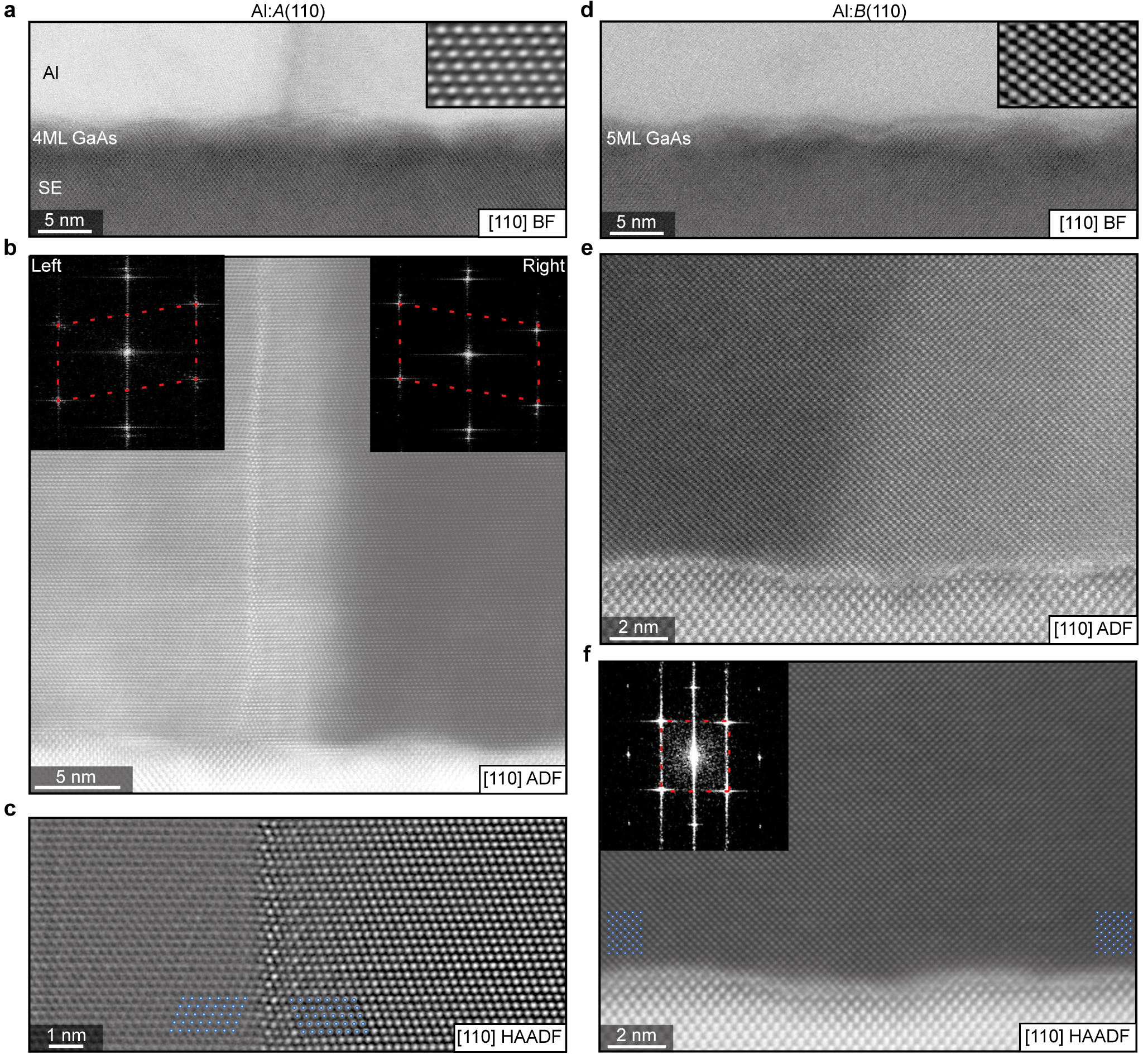
We observed this behaviour in samples where the InGaAs top barrier was capped with more than 3 MLs of GaAs. An example is shown in Fig 5, where the Al layer is locked in 5a as Al:(110) after capping with 4 MLs of GaAs and 5b as Al:(110) after capping with 5 MLs of GaAs. For the sample capped with 4 MLs GaAs in Fig. 5a, we observed that the Al only adapted the Al:(110) orientation. Surprisingly, we observed regions with abruptly changing Bright Field (BF) and ADF contrast in the STEM images. Yet, this contrast was not related to a major change in the crystal orientation, but to mirroring with respect to the Al(111) planes, as shown in Fig. 5b. This is apparent from the mirroring of the fast Fourier transform spectra and the atomic arrangement in the HAADF-STEM zoom-in in Fig. 5c. This implies that even when the whole Al film is locked as Al:{110}, the Al:(10) and Al:(10) are not degenerate in this grain orientation. Hence, the Al film in this crystal orientation is naturally prone to twinning and the related formation of incoherent grain boundaries.
This is different for a sample capped with 5 MLs of GaAs, shown in Fig. 5d, where the crystal orientation was locked into Al:(100). Similarly to the previous case, the lateral matching to the substrate was fixed as Al(110) to SE(110) for the whole layer. In this case, we detected only subtle differences in ADF and BF contrast, as shown in Fig. 5e. Such a detail in the acquired image of the Al layer corresponds to the region of the film with a change in contrast shown in the lower panel of Fig. 4a. These changes of contrast were sparse in the films and are likely related to subtle tilts of the crystal, as no apparent crystallographic change was seen in neither the HAADF-STEM image nor the fast Fourier transform in Fig. 5f. Compared to Al:, the symmetry of Al: type grain with respect to the {110} in-plane direction results in the formation of a fully single crystalline film. The subtle observed tilts might be related to relaxation of the strain induced by natural bending of the lamella for samples incorporating metamorphic buffer layers. We note that the differences in the capping layer thickness used in this study are at the experimental limits even with the utilized MBE technique. A consistent study of the capping layer thickness is needed in future works to gain full control over the Al grain growth selectivity.
In addition, we observed that the grain distribution in the films was affected by various additional factors, such as lamella preparation, strain, oxidation etc., which complicated the capability to perform consistent studies. Also, the Al film degraded and new grains appeared if the lamella was stored in ambient conditions for more over one month, indicating room temperature recrystallization in the films, as shown in the Supplemental Material sup .
V Effect of roughening on transport properties
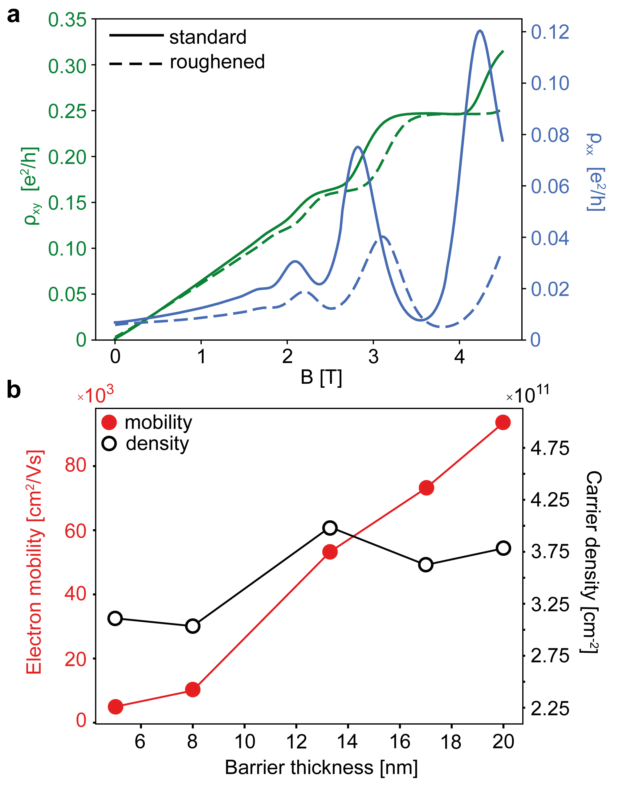
Even though the reduction of grain boundaries by surface roughening offers many benefits in terms of the crystal structure of the Al films, as discussed above, it is crucial to maintain the transport properties of the 2DEG. In Fig. 6a, we compare magneto-transport measurements of the roughened and standard materials. The measurements were performed in a van der Pauw configuration at 4 K on 5x5 mm as-grown samples after the Al film was removed by wet-etching. For the standard non-roughened surface we measured an electron mobility of 53 000 cm2/(Vs) at an electron density of 4.0 cm-2. For the sample with the same structure but intentionally roughened surface (5 MLs of GaAs) we measured 51 000 cm2/(Vs) at an electron density of 3.5 cm-2. The Drude mobility and charge carrier density do not significantly change for the roughened sample. We consider this difference to be negligible, since the properties and chemistry of the surface were reported to have a strong effect on the transport in shallow InAs 2DEGs Pauka et al. (2020); Hatke et al. (2017). We observed clear quantum Hall and Shubnikov-de Haas transport features at higher magnetic fields in both samples. The variation in quantum Hall behaviour at higher magnetic fields can be related to the difference in electron density and sample geometry, for example. In practical applications of the hybrid material, the rather low critical magnetic field of the superconducting aluminium typically limits the magnetic field range in transport experiments to below 1.5 T in a parallel field and tens of mT in a perpendicular field, where the behaviour of the compared materials is almost identical.
To further investigate the effect of the near-surface structure on the electron mobility, we grew a series of standard samples (capped with 2 MLs of GaAs) with the In0.75Ga0.25As top barrier thickness varying from 5 to 20 nm. The electron mobility increased almost linearly from 5 000 up to 100 000 cm2/(Vs) while the density remained between 3 and 4 cm-2, as shown in Fig. 6b. This demonstrates that the effect of the intentional roughening of the surface on the electron mobility is indeed negligible in comparison to the effect of other growth parameters and changes in the structural design. An enhancement in mobility is desirable, but an increase in the top barrier thickness can also affect the strength of the proximitized superconductivity, as will be discussed below and in the Supplemental Material sup .
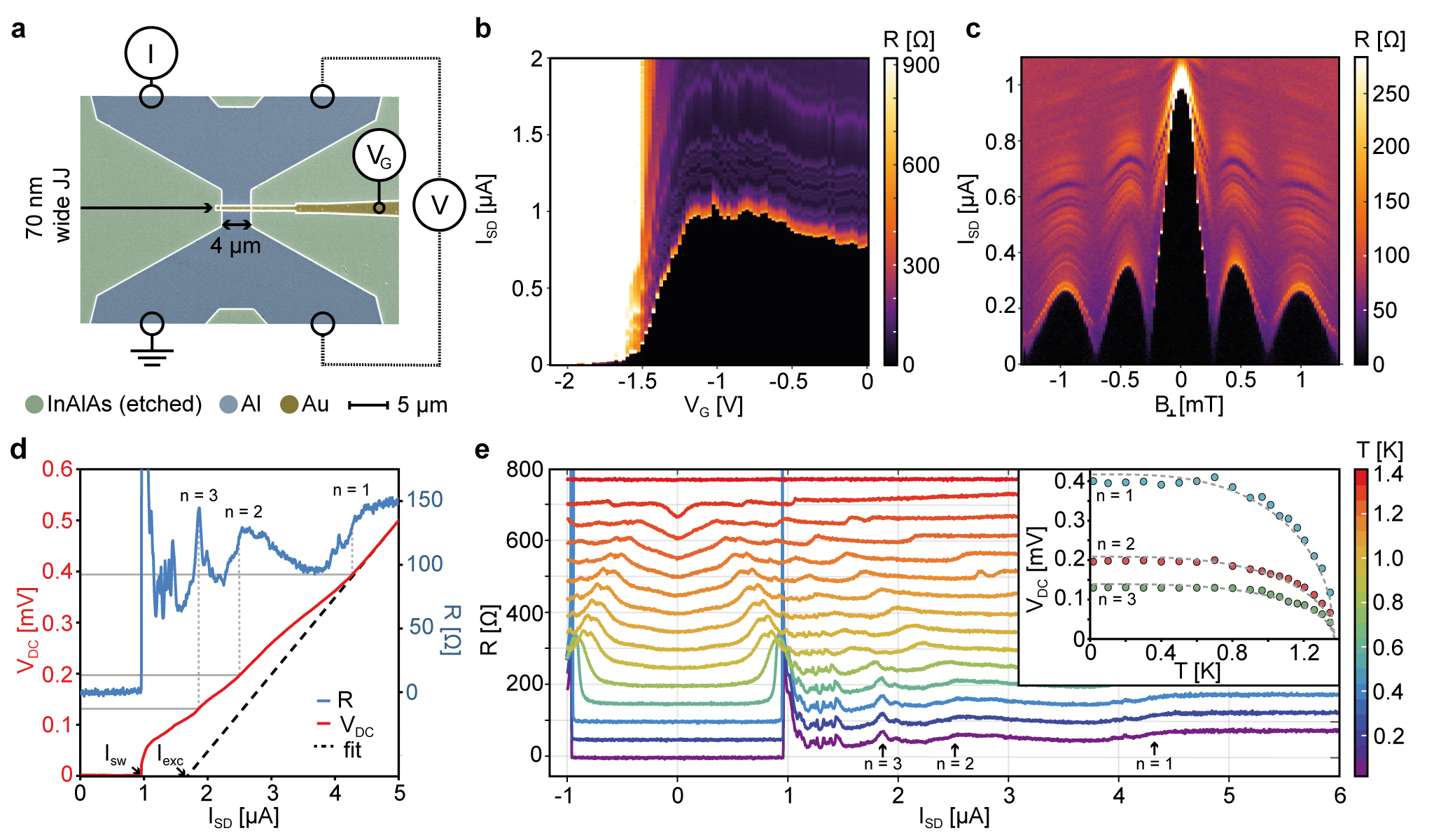
Finally, to assess the influence of the intentional roughening of the SE/SC interface on the superconducting properties of the proximitized system, we investigated the basic characteristics of a top-gated SC-normal-SC (SNS) planar Josephson junction (JJ) device, shown in Fig. 7a. The JJ device was defined by selectively etching Al (blue) to expose the III-V semiconductor below, which was controlled via an electrostatic gate (gold). The differential resistance = / as a function of bias current and top gate voltage , is shown in Fig. 7b. The transition from superconducting to the resistive state (at the switching current ) was tuned by sweeping , where full suppression of the supercurrent appeared around = -1.8 V. For all following experiments we set = -1.1 V where we expected the SE segment to be tuned to the single sub-band regime.
Next, we investigated the SC-to-normal transition as a function of the out-of-plane magnetic field . We observed a Fraunhofer pattern typical for planar JJs, shown in Fig. 7c. The suppression of the switching current occurs when the flux penetrating the junction area equals the magnetic flux quantum, as further discussed in the Supplemental Material sup . For large current bias the junction resistance attained a normal state value = 150 (the same as above the critical temperature of 1.38 K).
At zero magnetic field we found a maximum switching current 1 A, and excess current 1.7 A, as shown in Fig. 7d. Both the products and can be related to the interface transparency and the induced superconducting gap energy Flensberg et al. (1988); Kjærgaard et al. (2017). This is consistent with other reports in literature and discussed in more detail in the Supplementary Material sup .
The induced gap energy can also be extracted by analysing the modulation of the differential resistance in the resistive state. This originates from multiple Andreev reflection (MAR) and became apparent when the current bias was larger than the switching current for both the gate and magnetic field dependencies. The MAR is a signature of coherent charge transport at finite bias within the induced superconducting gap, *, i.e., at sub-gap voltages / ( = 210 eV) Flensberg et al. (1988); Kjærgaard et al. (2017). The position in of individual MAR peaks is related to the size of the induced gap, as shown in Fig. 7d-e. The induced gap * is given via = 2 , where = 1, 2, 3, … This is highlighted in Fig. 7d for a measurement at 18 mK. By averaging the value extracted for n = 1, 2 and 3, we found * = 197 2 eV which is close to the nominal . This value of * remains almost constant up to 700 mK, as apparent from the dependency of assigned to different on temperature shown 7e. Above 700 mK, * starts to change and follows the BCS relation Waldram (1996) for the Al gap energy = 2/.
To demonstrate the quality of the intentionally roughened material, we compared the measurements to a nominally identical JJ device fabricated from the standard non-roughened material (2 MLs of GaAs). The same analysis of MAR as introduced above yields *r = 197 1 eV for the roughened material and *s = 184 6 eV for the standard material, both at 500 mK. The similar values of * together with the no apparent change in electron mobility, show that the quality of the hybrid material is not significantly affected by the implemented roughening.
Furthermore, we investigated a JJ fabricated from the standard material where the top barrier thickness was increased from 13.4 nm to 20 nm (20 nm top barrier thickness and 2ML GaAs cap). In this case, we observed a reduced number of clear MAR features which complicated the correct assignment of , as shown in the Supplemental Material. The analysis yields an upper bound of *20nm = 170 eV for = 2 at 550 mK, which is lower but still comparable to the samples with a thinner barrier and unexpected in comparison to theoretical predictions Shabani et al. (2016). The possibility to increase the electron mobility (i.e. tune the top barrier thickness), while preserving the induced gap size can be advantageous in future device designs. More importantly, it was recently suggested by Awoga et al. Awoga et al. (2022), that a weaker coupling between the SE and SC can mitigate influence of local disorder, which is expected to be one of the significant factors that can impair device performance. More detailed analysis of the MAR data for all the investigate samples is given in the Supplemental Material sup . Our results show that more experimental investigations of growth series with consistent change of parameters are necessary to relate the material properties to current theoretical description of hybrid devices.
Overall, we found that all three material designs exhibited a highly transparent interface, gap size comparable to the BCS theory and other reports in literature, signatures of coherent ballistic transport through a JJ and a good performance in our other experiments focused on InAs/Al hybrids Haxell et al. (2022a, b); Hinderling et al. (2022). In addition, studying differently designed material structures implemented into hybrid devices is important for further understanding of the influence of individual material parameters on transport properties.
VI Conclusion
This work provides a full description of the growth of shallow high-quality InAs 2DEGs with epitaxial Al films by MBE. We have demonstrated that deposition of 5 MLs of GaAs on the top barrier anisotropically roughens the surface. Subsequent in-situ deposition of a thin epitaxial Al film results in the formation of an Al layer with a single crystal orientation, which remains free of grain boundaries on at least a 5 m scale. Our results also indicate that the intentional roughening can be further optimized to achieve full control over the crystallographic orientation of the Al film.
We found that the introduced roughening did not impair the electron mobility and carrier density of the shallow 2DEG. In addition, the material showed qualities comparable to state-of-the-art SE/SC hybrid JJ-based devices in transport experiments. This implies that local nanotexturing of the semiconductor surface (likely at scales below the Fermi wavelength) does not negatively impact the transport properties of the proximitized system, and provides new experimental insight into the requirements on quality of the interface in hybrid materials, which were recently subject of extensive debate Cole et al. (2016); Thomas et al. (2022).
Apart from the possibility of extending the enhanced epitaxy on roughened surfaces to other materials, control over the Al orientation has implications for interface engineering and chemical stability of the well-established hybrid InAs/Al structures. Most importantly, the removal of grain boundaries from the Al film allows for the possibility to form more complex and still fully epitaxial heterostructures on top of the Al. Finally, we hope that the extensive details of material synthesis provided in this work allows for reproducible growth of the material and make it widely accessible to the scientific community.
VII Acknowledgement
We thank Christian Reichl, Stefan Fält and Mattias Beck for technical support. We also thank Sjoerd Telkamp, Clemens Todt and Tilman Tröster for fruitful discussions. We thank the IBM Quantum Academic Network for financial support. We acknowledge the support of the Cleanroom Operations Team of the Binnig and Rohrer Nanotechnology Center (BRNC). This work was supported by the Swiss National Center of Competence in Research Quantum Science and Technology, QSIT, together with the European Union and the state of Berlin within the frame of the European Regional Development Fund (ERDF) under project number 2016011843 and by Czech Science Foundation grant number 22-22000M. F. N. acknowledges support from the European Research Council grant number 804273 and the Swiss National Science Foundation grant number 200021 201082.
References
- Hays et al. (2021) M. Hays, V. Fatemi, D. Bouman, J. Cerrillo, S. Diamond, K. Serniak, T. Connolly, P. Krogstrup, J. Nygård, A. Levy Yeyati, et al., Science 373, 430 (2021).
- Larsen et al. (2015) T. W. Larsen, K. D. Petersson, F. Kuemmeth, T. S. Jespersen, P. Krogstrup, J. Nygård, and C. M. Marcus, Physical Review Letters 115, 127001 (2015).
- Casparis et al. (2018) L. Casparis, M. R. Connolly, M. Kjaergaard, N. J. Pearson, A. Kringhøj, T. W. Larsen, F. Kuemmeth, T. Wang, C. Thomas, S. Gronin, et al., Nature nanotechnology 13, 915 (2018).
- Sarma et al. (2015) S. D. Sarma, M. Freedman, and C. Nayak, npj Quantum Information 1, 1 (2015).
- Krogstrup et al. (2015) P. Krogstrup, N. Ziino, W. Chang, S. Albrecht, M. Madsen, E. Johnson, J. Nygård, C. M. Marcus, and T. Jespersen, Nature Materials 14, 400 (2015).
- Shabani et al. (2016) J. Shabani, M. Kjærgaard, H. J. Suominen, Y. Kim, F. Nichele, K. Pakrouski, T. Stankevic, R. M. Lutchyn, P. Krogstrup, R. Feidenhans, et al., Physical Review B 93, 155402 (2016).
- Mikkelsen et al. (2018) A. E. Mikkelsen, P. Kotetes, P. Krogstrup, and K. Flensberg, Physical Review X 8, 031040 (2018).
- Chang et al. (2015) W. Chang, S. Albrecht, T. Jespersen, F. Kuemmeth, P. Krogstrup, J. Nygård, and C. M. Marcus, Nature nanotechnology 10, 232 (2015).
- Mourik et al. (2012) V. Mourik, K. Zuo, S. M. Frolov, S. Plissard, E. P. Bakkers, and L. P. Kouwenhoven, Science 336, 1003 (2012).
- Vaitiekėnas et al. (2020) S. Vaitiekėnas, G. Winkler, B. van Heck, T. Karzig, M.-T. Deng, K. Flensberg, L. Glazman, C. Nayak, P. Krogstrup, R. Lutchyn, et al., Science 367, eaav3392 (2020).
- Kurtossy et al. (2021) O. Kurtossy, Z. Scherübl, G. Fülöp, I. E. Lukács, T. Kanne, J. Nygård, P. Makk, and S. Csonka, Nano Letters 21, 7929 (2021).
- Friedl et al. (2018) M. Friedl, K. Cerveny, P. Weigele, G. Tütüncüoglu, S. Martí-Sánchez, C. Huang, T. Patlatiuk, H. Potts, Z. Sun, M. O. Hill, et al., Nano Letters 18, 2666 (2018).
- Krizek et al. (2018) F. Krizek, J. E. Sestoft, P. Aseev, S. Marti-Sanchez, S. Vaitiekėnas, L. Casparis, S. A. Khan, Y. Liu, T. Stankevič, A. M. Whiticar, et al., Physical Review Materials 2, 093401 (2018).
- Aghaee et al. (2022) M. Aghaee, A. Akkala, Z. Alam, R. Ali, A. A. Ramirez, M. Andrzejczuk, A. E. Antipov, M. Astafev, B. Bauer, J. Becker, et al., arXiv preprint arXiv:2207.02472 (2022).
- Sarney et al. (2018) W. L. Sarney, S. P. Svensson, K. S. Wickramasinghe, J. Yuan, and J. Shabani, Journal of Vacuum Science & Technology B, Nanotechnology and Microelectronics: Materials, Processing, Measurement, and Phenomena 36, 062903 (2018).
- Sarney et al. (2020) W. L. Sarney, S. P. Svensson, A. C. Leff, W. F. Schiela, J. O. Yuan, M. C. Dartiailh, W. Mayer, K. S. Wickramasinghe, and J. Shabani, Journal of Vacuum Science & Technology B, Nanotechnology and Microelectronics: Materials, Processing, Measurement, and Phenomena 38, 032212 (2020).
- Wang et al. (2020) T. Wang, C. Thomas, R. E. Diaz, S. Gronin, D. Passarello, G. C. Gardner, M. A. Capano, and M. J. Manfra, Journal of Crystal Growth 535, 125570 (2020).
- Ferguson et al. (2007) A. Ferguson, R. Clark, et al., Superconductor Science and Technology 21, 015013 (2007).
- Pracht et al. (2016) U. S. Pracht, N. Bachar, L. Benfatto, G. Deutscher, E. Farber, M. Dressel, and M. Scheffler, Physical Review B 93, 100503 (2016).
- Nguyen et al. (2018) L. Nguyen, T. Hashimoto, D. N. Zakharov, E. A. Stach, A. P. Rooney, B. Berkels, G. E. Thompson, S. J. Haigh, and T. L. Burnett, ACS Applied Materials & Interfaces 10, 2230 (2018).
- David Henry et al. (2014) M. David Henry, S. Wolfley, T. Monson, B. G. Clark, E. Shaner, and R. Jarecki, Journal of Applied Physics 115, 083903 (2014).
- Kjærgaard et al. (2016) M. Kjærgaard, F. Nichele, H. Suominen, M. Nowak, M. Wimmer, A. Akhmerov, J. Folk, K. Flensberg, J. Shabani, w. C. Palmstrøm, et al., Nature Communications 7, 1 (2016).
- Richardson et al. (2016) C. J. Richardson, N. P. Siwak, J. Hackley, Z. K. Keane, J. E. Robinson, B. Arey, I. Arslan, and B. S. Palmer, Superconductor Science and Technology 29, 064003 (2016).
- de Leon et al. (2021) N. P. de Leon, K. M. Itoh, D. Kim, K. K. Mehta, T. E. Northup, H. Paik, B. Palmer, N. Samarth, S. Sangtawesin, and D. Steuerman, Science 372, eabb2823 (2021).
- Cole et al. (2016) W. S. Cole, J. D. Sau, and S. D. Sarma, Physical Review B 94, 140505 (2016).
- Thomas et al. (2022) S. N. Thomas, S. D. Sarma, and J. D. Sau, Physical Review B 106, 174501 (2022).
- Thomas et al. (2019) C. Thomas, R. E. Diaz, J. H. Dycus, M. E. Salmon, R. E. Daniel, T. Wang, G. C. Gardner, and M. J. Manfra, Physical Review Materials 3, 124202 (2019).
- Moehle et al. (2021) C. M. Moehle, C. T. Ke, Q. Wang, C. Thomas, D. Xiao, S. Karwal, M. Lodari, V. van de Kerkhof, R. Termaat, G. C. Gardner, et al., Nano Letters 21, 9990 (2021).
- Weilmeier et al. (1991) M. Weilmeier, K. Colbow, T. Tiedje, T. v. Buuren, and L. Xu, Canadian Journal of Physics 69, 422 (1991).
- (30) See Supplemental Material at [URL will be inserted by publisher] for following details: Methods; S1: Surface of shallow InAs 2DEGs; S2: Extraction of lattice spacings; S3: Controlled oxidation of Al; S4: In-situ annealing STEM experiment; S5: Ageing of studied lamellae; S6: STEM tomography, S7: Additional analysis of the JJ measurements of the roughened sample, S8: JJ measurements of the standard non-roughened samples. .
- Haxell et al. (2022a) D. Haxell, E. Cheah, F. Křížek, R. Schott, M. Ritter, M. Hinderling, W. Belzig, C. Bruder, W. Wegscheider, H. Riel, et al., arXiv preprint arXiv:2204.05619 (2022a).
- Haxell et al. (2022b) D. Haxell, M. Coraiola, D. Sabonis, M. Hinderling, S. ten Kate, E. Cheah, F. Krizek, R. Schott, W. Wegscheider, W. Belzig, et al., arXiv preprint arXiv:2212.03554 (2022b).
- Hinderling et al. (2022) M. Hinderling, D. Sabonis, S. Paredes, D. Haxell, M. Coraiola, S. ten Kate, E. Cheah, F. Krizek, R. Schott, W. Wegscheider, et al., arXiv preprint arXiv:2212.11164 (2022).
- Nicolai et al. (2021) L. Nicolai, K. Biermann, and A. Trampert, Ultramicroscopy 224, 113261 (2021).
- Ohta et al. (1989) K. Ohta, T. Kojima, and T. Nakagawa, Journal of Crystal Growth 95, 71 (1989).
- Dieguez et al. (1997) A. Dieguez, A. Vila, A. Cornet, S. Clark, D. Westwood, and J. Morante, Journal of Vacuum Science & Technology B: Microelectronics and Nanometer Structures Processing, Measurement, and Phenomena 15, 687 (1997).
- Chen et al. (2018) Y. Chen, Z. Chen, J. Li, Y. Chen, C. Li, J. Zhan, T. Yu, X. Kang, F. Jiao, S. Li, et al., CrystEngComm 20, 6811 (2018).
- Feng et al. (2016) X. Feng, T. Yu, Y. Wei, C. Ji, Y. Cheng, H. Zong, K. Wang, Z. Yang, X. Kang, G. Zhang, et al., ACS Applied Materials & Interfaces 8, 18208 (2016).
- Pauka et al. (2020) S. Pauka, J. Witt, C. Allen, B. Harlech-Jones, A. Jouan, G. Gardner, S. Gronin, T. Wang, C. Thomas, M. Manfra, et al., Journal of Applied Physics 128, 114301 (2020).
- Hatke et al. (2017) A. Hatke, T. Wang, C. Thomas, G. Gardner, and M. Manfra, Applied Physics Letters 111, 142106 (2017).
- Flensberg et al. (1988) K. Flensberg, J. B. Hansen, and M. Octavio, Physical Review B 38, 8707 (1988).
- Kjærgaard et al. (2017) M. Kjærgaard, H. J. Suominen, M. Nowak, A. Akhmerov, J. Shabani, C. Palmstrøm, F. Nichele, and C. M. Marcus, Physical Review Applied 7, 034029 (2017).
- Waldram (1996) J. R. Waldram, Superconductivity of metals and cuprates (IOP Publishing Ltd, 1996).
- Awoga et al. (2022) O. A. Awoga, M. Leijnse, A. M. Black-Schaffer, and J. Cayao, arXiv preprint arXiv:2212.06061 (2022).