Possible realization of hyperbolic plasmons in a few-layered rhenium disulfide
Abstract
The in-plane structural anisotropy in low-symmetric layered compound rhenium disulfide () makes it a candidate to host and tune electromagnetic phenomena specific for anisotropic media. In particular, optical anisotropy may lead to the appearance of hyperbolic plasmons, a highly desired property in optoelectronics. The necessary condition is a strong anisotropy of the principal components of the dielectric function, such that at some frequency range, one component is negative and the other is positive, i.e., one component is metallic, and the other one is dielectric. Here, we study the effect of anisotropy in and show that it can be a natural material to host hyperbolic plasmons in the ultraviolet frequency range. The operating frequency range of the hyperbolic plasmons can be tuned with the number of layers.
I Introduction
The rise of hyperbolic materials in recent years promises important applications in optoelectronics and nanophotonics [1, 2, 3, 4, 5]. Light can acquire hyperbolic dispersion while passing through such materials, which occurs in some frequency range, when different principal components of the longitudinal dielectric function (dielectric permittivity) have opposite signs. For the case of isotropic medium, it behaves as a dielectric, that is, supports propagating electromagnetic waves, when the sign of the dielectric function is positive. When the latter is negative, the incident light is reflected, with only an exponentially decaying evanescent field penetrating the material, like for metals below plasma threshold.
Anisotropy in electronic, optical, vibrational, and transport behaviour can occur when structural anisotropy is present, and if it is sufficiently strong, the different components of the dielectric permittivity tensor may aquire opposite signs to turn the material hyperbolic. In two-dimensional crystals, in-plane anisotropy strong enough to make it hyperbolic is a unique situation that allows to confine short wavelengths (large wave vectors) inside a material, promising smaller sizes for optoelectronic devices. Optical anisotropy in rhenium disulfide () has been established both for bulk crystals [6, 7] and for thin layers [8]. In this work we predict that () that appears in a distorted 1T phase can realize hyperbolic plasmons depending on the number of layers.
It has been suggested that anisotropic 2D materials can be tuned to become hyperbolic via electrostatic tuning, strain or dimensionality and can host hyperbolic plasmons [9, 10]. Several studies [11, 12, 13] have investigated hyperbolic plasmons (HP) and its existence in naturally occurring materials. The strong anisotropy of hints at its potential as a natural hyperbolic material, offering possibilities for studying HP. Previous works [14, 15] have studied the band structure and anisotropic optical response of , but the study of HP remains largely unexplored. Here we use the ladder-vertex corrected and local-field corrected plasmonic response in ReS2 within a self-consistent solution of Bethe-Salpeter equation (BSE) as implemented in Questaal [16].
The rest of the paper is organized as follows. In Sec. II.1, we describe the anisotropic atomic structure of and in Sec. II.2, we briefly describe theoretical methods and provide computational details. In Secs. III.1 and III.2 we present our results on the electronic structure and optical properties of . In Sec. IV, we briefly summarize our results and conclude the paper.
II Atomic Structure and Computational Details
II.1 Atomic structure
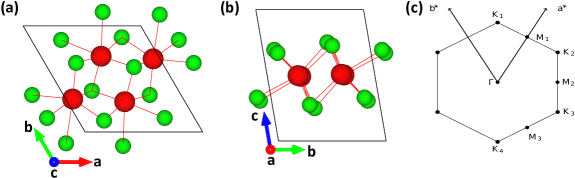
belongs to the family of two-dimensional (2D) layered transition metal dichalcogenide (TMDs) of the form where M is a transition metal atom (Mo, W, Re, …) and X is a group-16 atom (S, Se, Te). The atomic structure of layers has neither H or T character. Unlike other TMDs, which usually have 1H or 1T structure in their ground state, crystallizes in a distorted-1T structure with clustering of Re units forming parallel metal chains along the van der Waals plane (see Fig. 1).
The compound belongs to the triclinic symmetry group , resembling a distorted CdCl2 structure. It comprises three atomic layers, S-Re-S, where covalent bonds join Re and S. The adjacent layers of are coupled by weak van der Waals (vdW) forces to form bulk crystals. The unit cell is derived from hexagonal symmetry towards a distorted 1T structure, in which Re atoms group into parallelograms of four Re atoms. The formation of Re chains breaks the hexagonal symmetry and doubles the unit cell size. Hence the unit cell of single layer in the distorted-1T phase is composed of four Re and eight S atoms. In pristine , the valence band maximum is composed from 5d orbitals of Re atoms and 3p orbitals of S atoms, and the conduction band minimum is derived from 5d orbitals of Re atoms. The Brillouin zone of the is hexagonal but with unequal sides as a result of the distorted atomic structure. Energy band structures were generated along the symmetry lines shown in Fig. 1.
II.2 Computational Details
II.2.1 LDA, QSGW, and QSG self-consistency
Single-particle calculations (LDA, and the the quasi-particle self-consistent GW [18] (QSGW) self-energy ) were performed on a points (Monkhorst pack) for bulk and for ML and BL. An energy cutoff of 400 was used and Gaussian smearing with a width of 0.05 . The tolerance of and has been taken in convergence of energy and RMS density respectively. The charge density was made self-consistent for each iteration in the QSGW self-consistency cycle. The QSGW cycle was iterated until the RMS change in reached Ry. Thus the calculation was self-consistent in both and the density. Numerous checks were made to verify that the self-consistent (k) was independent of starting point. For ML-, we performed a rigorous check for vacuum correction to all band gap and dielectric screening by increasing the size from to . Since along the z-direction we have a vacuum, the dielectric constant, which is the real part of the macroscopic dielectric response at , should be close to unity.
In the present work, the electron-hole two-particle correlations are incorporated within a self-consistent ladder BSE implementation [19] with Tamn-Dancoff approximation [20]. Ladder diagrams are included in the polarizability that makes , via the solution of a Bethe-Salpeter equation (BSE); thus this form of goes beyond the RPA in constructing the self-energy . The electron-hole attraction from the ladders enhances , thus reducing , which in turn reduces the bandgap. A static vertex is used to construct . G and W are calculated self-consistently, in quasiparticlized form [18]: G and W are updated iteratively until all of them converge (QSGW). When ladders are incorporated into W, we denote the process as QS to signify was computed from the BSE. The macroscopic dielectric function we present here, , is also computed with the BSE.
The tetrahedron method is employed for integration over the Brillouin zone to calculate the optical spectrum. When calculating the dielectric response within BSE, the valence and conduction states that form the two-particle Hamiltonian are increased until the two-particle eigenvalues converge within an accuracy of 10 meV. For ReS2 the excitons are essentially Wannier-Mott [21] in nature and only the states at the valence band top and conduction band bottom contribute to their formation, so the convergence in the two-particle Hamiltonian size is much faster compared to the cases of CrX3 [22] where the excitons have Frenkel character and many valence and conductions bands over several electron volts form them. However, for the present work, our focus is the plasmonic response, while we will note the excitonic binding energies in different layered variants later.
Table (1) contains the lattice parameters for used throughout the calculations.
| Structure | a() | b() | c() | (°) | (°) | (°) |
| Bulk | 6.41695 | 6.52047 | 7.28252 | 91.8128 | 103.5630 | 118.8390 |
| ML | 6.41910 | 6.52306 | 45 | 90.7434 | 95.7909 | 118.8366 |
| BL | 6.41910 | 6.52306 | 28.66062 | 84.0127 | 89.7412 | 61.1634 |
| Band Gap() | |||
| Theory | LDA | QSGW | QSG |
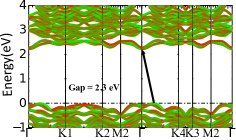
| Bulk | 1.15 | 1.75 | 1.7 |
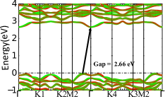
| ML | 1.29 | 2.75 | 2.66 |
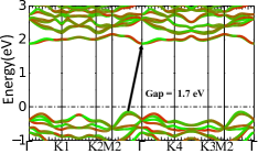
| BL | 1.23 | 2.35 | 2.3 |
III Results and Discussions
III.1 Quasiparticle Energies and Band Structure
| Dielectric Constant () | |||||
| Plasmonic frequency range () | Exciton Binding energy () | ||||
|---|---|---|---|---|---|
| Bulk | 9.67 | 9.37 | 6.21 | 6.02 - 6.78 (0.76) | - |
| BL | 6.97 | 7.09 | 2.66 | 6.65 - 7.08 (0.43) | 0.3 |
| ML | 2.97 | 3.19 | 1.42 | - | 0.74 |
The nature of the bandgap of has been widely debated in the literature. In a typical TMD family, the bandgap is direct when their thickness is reduced to the monolayer, ensuring that coupling with light is strong. One study from 2014 [23] reported direct bandgap for bulk ReS2, thus generating considerable interest in the system. However, both older studies such as [24, 25] and more recent studies such as [26, 27] report that the bulk is an indirect-bandgap semiconductor.
The electronic band structures (with spin-orbit coupling included) for bulk, BL and ML are shown in Fig. 2 and the band gaps at different levels of theory are summarized in Table 2. The free-standing ML of has been simulated for these calculations with the parameters shown in Table 1. Similar to prior work on monolayers of chromium trihalides [28], we check for convergence and scaling of band gap and the dielectric constant with vacuum size. We obtain the LDA band gap of which is significantly lower than the QSGW band gap of . LDA is known to underestimate the band gaps in semiconductors, and the enhancement in the QSGW band gap relative to LDA is standard [18]. QSGW usually overcorrects the gap because W is universally too large within the random phase approximation (RPA), and for the same reason it underestimates the dielectric constant [19]. Adding ladders largely eliminates both tendencies. In the present case extending causes only a modest reduction in the gap, to , suggesting insignificant corrections to the self-energy originating from BSE. This result is consistent with previous theoretical work [29] on ML-. The self-energy and the reduced screening increase the band gap and modify the band topology, which is observed in the ML-. The band gap at the level of LDA is direct, but the two-particle interactions lower the valence band maxima (VBM), which was at the point by about . A similar kind of change in band topology has been observed for in [29] but is absent in other some theoretical work [14].
We obtain a similar band topology in bulk and BL variants of ; however, the band gap values are and respectively. The nature of band gap in is different from more commonly studied semiconducting TMDs (e.g., MoS2, WS2, etc.), where the bulk and few-layer variants show indirect band gap and ML is direct. In this work, we observe a direct band gap at the LDA level and an indirect band gap for all the variants at the QSG level. This nature of the quasiparticle band gap does not conflict with experimental measurement because, different from our calculated free-standing cases, these measured samples are on substrates and are inevitably doped. The resulting self-energy corrections will be reduced under these conditions, resulting in a slightly indirect band gap for the measured samples. We note that the direct to indirect transition may not be sharp because the energy difference between the direct and indirect gap is small and external perturbations can affect the conclusion. However, our observations on the indirect nature of the band gap is important for many reasons. In most monolayer TMDs, the gap is direct and it makes them sufficiently bright and also the electron-hole radiative lifetimes are extremely small (often in picoseconds). While in systems with indirect band gaps, radiative and non-radiative processes compete, since the indirect states have longer lifetimes making them candidates for optoelectronics and photovoltaics [30].
III.2 Optical Absorption Spectra : Hyperbolic Plasmons
The anisotropic optical absorption has been previously studied using DFT [31]. Experimentally [26] it is demonstrated that the reduced crystal symmetry of leads to anisotropic optical properties that persist from the bulk down to the monolayer limit. The absence of excitonic correlations and underestimated band gaps in LDA studies hide several physical consequences in . Advanced theoretical studies such as [29] tackle anisotropic optical responses at the BSE level for monolayer , where ladder vertex corrected optical properties are computed on top of a single shot DFT based G0W0 one-particle description.
The large structural anisotropy in 2D materials, for example, a 4:3 anisotropy of the in-plane lattice constants in black phosphorus [9] and solid nitrogen [32, 33, 34]) makes them perfect candidates for hyperbolic materials and a natural place to look for HP. This offers new possibilities as hyperbolic materials showcase a wide variety of interesting properties, such as modes which transport heat by photon tunnelling with a high efficiency close to the theoretical limit[35], and broadband absorption [36]. We first define the condition for hyperbolicity. The hyperbolic region appears when
| (1) |
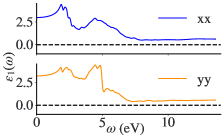
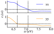
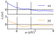
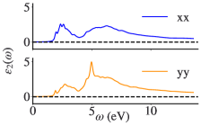
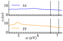
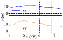
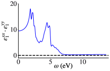
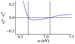
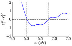
where, and are the real part of the dielectric response along the x and y direction respectively. We assume that by symmetry and, thus, and are the principal directions of the dielectric permeattivity. For different variants of , the real and imaginary part of dielectric response is plotted in Fig. 3. We observe that significant difference in optical response for incident polarized light along different directions. While ML- (Fig. 3, left panel), hosts some strongly bound anisotropic excitons deep inside the one-particle gap, HP are absent. For the BL- (Fig. 3, center panel), the Re() goes to negative at , which results in a hyperbolic region starting at that frequency with an energy window of . For bulk- this energy window increases to . The sign change is key to the appearance of the hyperbolic region and it becomes more apparent in Fig. 4 where we plot the product which becomes negative in the energy window. remains large for both bulk and BL in the hyperbolic energy window suggesting large damping of the HP. In the BL, these plasmons are less damped compared to bulk. Also, note that these HP in ReS2 are in ultraviolet range, in contrast to the infrared HP in CuS nanocrystals [13].
The inherent anisotropy in ReS2 provides an opportunity to tune its magnitude by applying strain. We apply uni-directional strains () along and respectively and explore the hyperbolic region. We apply up to 4% strain and see that the ML never hosts HP. However, in bulk on application of compressive unidirectional strain () along , the HP window increases upto 1.3 eV. This enhanced HPs also have lesser damping compared to the un-strained compound. On the other hand, reduces the HP window. In the BL, application of , almost entirely kills the HP window while enhances the HP window and also hosts less damped plasmonic modes. In short, we observe that while strain can be used to tune the hyperbolic energy window and the lifetimes of the plasmons, we could not produce HPs in the monolayer sample under any condition. However, the HPs remain pretty robust in both the bulk and BL variants, also their stability could be enhanced on selective applications of uni-directional strain.
IV Conclusion
Anisotropy is a key to tuning material properties. Discontinuities at surfaces, residual strains and metamaterials have been used as platforms for realizing anisotropic optical properties. Naturally occurring structurally anisotropic materials are not necessarily hyperbolic always.
In this work we show that the structural anisotropy in , even though much weaker compared to materials like black Phosphorus and solid Nitrogen, leads to the occurrence of hyperbolic plasmons in a narrow energy window. The plasmonic resonances can be tuned by controlling the number of layers in the far ultraviolet frequency range. The ability of such a tunability of the plasmons opens up new opportunities in regard to optoelectronic devices. We further show that the hyperbolic region and its stability can be enhanced by unidirectional strains.
V Acknowledgement
MIK and SA are supported by the ERC Synergy Grant, project 854843 FASTCORR (Ultrafast dynamics of correlated electrons in solids). MvS and DP were supported by the Computational Chemical Sciences program within the Office of Basic Energy Sciences, U.S. DOE under Contract No. DE-AC36-08GO28308. This research used resources of the National Energy Research Scientific Computing Center (NERSC), award BES-ERCAP0021783, under DOE Contract No. DE-AC02-05CH11231. We acknowledge PRACE for awarding us access to Irene-Rome hosted by TGCC, France and Juwels Booster and Cluster, Germany.
References
- Poddubny et al. [2013] A. Poddubny, I. Iorsh, P. Belov, and Y. Kivshar, Hyperbolic metamaterials, Nature photonics 7, 948 (2013).
- Cortes et al. [2012] C. Cortes, W. Newman, S. Molesky, and Z. Jacob, Quantum nanophotonics using hyperbolic metamaterials, Journal of Optics 14, 063001 (2012).
- Shekhar et al. [2014] P. Shekhar, J. Atkinson, and Z. Jacob, Hyperbolic metamaterials: fundamentals and applications, Nano convergence 1, 1 (2014).
- Ferrari et al. [2015] L. Ferrari, C. Wu, D. Lepage, X. Zhang, and Z. Liu, Hyperbolic metamaterials and their applications, Progress in Quantum Electronics 40, 1 (2015).
- Códova-Castro et al. [2019] R. M. Códova-Castro, M. Casavola, M. van Schilfgaarde, A. Krasavin, M. A. Green, D. Richards, and A. Zayats, Anisotropic Plasmonic CuS Nanocrystals as a Natural Electronic Material with Hyperbolic Optical Dispersion, ACS Nano. 13, 6550 (2019).
- Lin et al. [2011] D. Y. Lin, T. P. Huang, F. L. Wu, C. M. Lin, Y. S. Huang, and K. K. Tiong, Anisotropy of photoluminescence in layered semiconductors ReS2 and ReS2: Au, in Solid State Phenomena, Vol. 170 (Trans Tech Publ, 2011) pp. 135–138.
- Friemelt et al. [1993] K. Friemelt, M.-C. Lux-Steiner, and E. Bucher, Optical properties of the layered transition-metal-dichalcogenide ReS2: anisotropy in the van der waals plane, Journal of applied physics 74, 5266 (1993).
- Liu et al. [2015] E. Liu, Y. Fu, Y. Wang, Y. Feng, H. Liu, X. Wan, W. Zhou, B. Wang, L. Shao, C.-H. Ho, et al., Integrated digital inverters based on two-dimensional anisotropic ReS2 field-effect transistors, Nature communications 6, 1 (2015).
- Nemilentsau et al. [2016] A. Nemilentsau, T. Low, and G. Hanson, Anisotropic 2D materials for tunable hyperbolic plasmonics, Physical review letters 116, 066804 (2016).
- Van Veen et al. [2019] E. Van Veen, A. Nemilentsau, A. Kumar, R. Roldán, M. I. Katsnelson, T. Low, and S. Yuan, Tuning two-dimensional hyperbolic plasmons in black phosphorus, Physical Review Applied 12, 014011 (2019).
- Low et al. [2017] T. Low, A. Chaves, J. D. Caldwell, A. Kumar, N. X. Fang, P. Avouris, T. F. Heinz, F. Guinea, L. Martin-Moreno, and F. Koppens, Polaritons in layered two-dimensional materials, Nature materials 16, 182 (2017).
- Sun et al. [2014] J. Sun, N. M. Litchinitser, and J. Zhou, Indefinite by nature: from ultraviolet to terahertz, Acs Photonics 1, 293 (2014).
- Córdova-Castro et al. [2019] R. M. Córdova-Castro, M. Casavola, M. Van Schilfgaarde, A. V. Krasavin, M. A. Green, D. Richards, and A. V. Zayats, Anisotropic plasmonic cus nanocrystals as a natural electronic material with hyperbolic optical dispersion, ACS nano 13, 6550 (2019).
- Echeverry and Gerber [2018] J. Echeverry and I. Gerber, Theoretical investigations of the anisotropic optical properties of distorted 1T ReS2 and ReSe2 monolayers, bilayers, and in the bulk limit, Physical Review B 97, 075123 (2018).
- Zhang et al. [2015] E. Zhang, Y. Jin, X. Yuan, W. Wang, C. Zhang, L. Tang, S. Liu, P. Zhou, W. Hu, and F. Xiu, ReS2-based field-effect transistors and photodetectors, Advanced Functional Materials 25, 4076 (2015).
- Pashov et al. [2020] D. Pashov, S. Acharya, W. R. Lambrecht, J. Jackson, K. D. Belashchenko, A. Chantis, F. Jamet, and M. van Schilfgaarde, Questaal: A package of electronic structure methods based on the linear muffin-tin orbital technique, Computer Physics Communications 249, 107065 (2020).
- Momma and Izumi [2011] K. Momma and F. Izumi, Vesta 3 for three-dimensional visualization of crystal, volumetric and morphology data, Journal of applied crystallography 44, 1272 (2011).
- van Schilfgaarde et al. [2006] M. van Schilfgaarde, T. Kotani, and S. Faleev, Quasiparticle self-consistent GW theory, Physical review letters 96, 226402 (2006).
- Cunningham et al. [2018] B. Cunningham, M. Grüning, P. Azarhoosh, D. Pashov, and M. Van Schilfgaarde, Effect of ladder diagrams on optical absorption spectra in a quasiparticle self-consistent gw framework, Physical Review Materials 2, 034603 (2018).
- Hirata and Head-Gordon [1999] S. Hirata and M. Head-Gordon, Time-dependent density functional theory within the tamm–dancoff approximation, Chemical Physics Letters 314, 291 (1999).
- Qiu et al. [2013] D. Y. Qiu, H. Felipe, and S. G. Louie, Optical spectrum of mos 2: many-body effects and diversity of exciton states, Physical review letters 111, 216805 (2013).
- Acharya et al. [2022] S. Acharya, D. Pashov, A. N. Rudenko, M. Rösner, M. v. Schilfgaarde, and M. I. Katsnelson, Real-and momentum-space description of the excitons in bulk and monolayer chromium tri-halides, npj 2D Materials and Applications 6, 1 (2022).
- Tongay et al. [2014] S. Tongay, H. Sahin, C. Ko, A. Luce, W. Fan, K. Liu, J. Zhou, Y.-S. Huang, C.-H. Ho, J. Yan, et al., Monolayer behaviour in bulk ReS2 due to electronic and vibrational decoupling, Nature communications 5, 1 (2014).
- Ho et al. [1997a] C. Ho, P. Liao, Y. Huang, T.-R. Yang, and K.-K. Tiong, Optical absorption of ReS2 and ReSe2 single crystals, Journal of applied physics 81, 6380 (1997a).
- Ho et al. [1997b] C. Ho, P. Liao, Y. Huang, and K.-K. Tiong, Temperature dependence of energies and broadening parameters of the band-edge excitons of ReS2 and ReSe2, Physical Review B 55, 15608 (1997b).
- Aslan et al. [2016] O. B. Aslan, D. A. Chenet, A. M. Van Der Zande, J. C. Hone, and T. F. Heinz, Linearly polarized excitons in single-and few-layer ReS2 crystals, Acs Photonics 3, 96 (2016).
- Gutiérrez-Lezama et al. [2016] I. Gutiérrez-Lezama, B. A. Reddy, N. Ubrig, and A. F. Morpurgo, Electroluminescence from indirect band gap semiconductor ReS2, 2D Materials 3, 045016 (2016).
- Acharya et al. [2021] S. Acharya, D. Pashov, B. Cunningham, A. N. Rudenko, M. Rösner, M. Grüning, M. van Schilfgaarde, and M. I. Katsnelson, Electronic structure of chromium trihalides beyond density functional theory, Physical Review B 104, 155109 (2021).
- Zhong et al. [2015] H.-X. Zhong, S. Gao, J.-J. Shi, and L. Yang, Quasiparticle band gaps, excitonic effects, and anisotropic optical properties of the monolayer distorted 1 t diamond-chain structures ReS2 and ReSe2, Physical Review B 92, 115438 (2015).
- Grzeszczyk et al. [2022] M. Grzeszczyk, K. Novoselov, and M. Koperski, ZnPSe3 as ultrabright indirect band-gap system with microsecond excitonic lifetimes, Proceedings of the National Academy of Sciences 119, e2207074119 (2022).
- Ho and Huang [2004] C. Ho and C. Huang, Optical property of the near band-edge transitions in rhenium disulfide and diselenide, Journal of alloys and compounds 383, 74 (2004).
- Rudenko et al. [2022] A. N. Rudenko, S. Acharya, F. Tasnádi, D. Pashov, A. V. Ponomareva, M. Van Schilfgaarde, I. A. Abrikosov, and M. I. Katsnelson, Electronic and optical properties of crystalline nitrogen versus black phosphorus: A comparative first-principles study, Physical Review B 105, 205135 (2022).
- Ji et al. [2020] C. Ji, A. A. Adeleke, L. Yang, B. Wan, H. Gou, Y. Yao, B. Li, Y. Meng, J. S. Smith, V. B. Prakapenka, et al., Nitrogen in black phosphorus structure, Science advances 6, eaba9206 (2020).
- Laniel et al. [2020] D. Laniel, B. Winkler, T. Fedotenko, A. Pakhomova, S. Chariton, V. Milman, V. Prakapenka, L. Dubrovinsky, and N. Dubrovinskaia, High-pressure polymeric nitrogen allotrope with the black phosphorus structure, Phys. Rev. Lett. 124, 216001 (2020).
- Biehs et al. [2012] S.-A. Biehs, M. Tschikin, and P. Ben-Abdallah, Hyperbolic metamaterials as an analog of a blackbody in the near field, Physical review letters 109, 104301 (2012).
- Riley et al. [2017] C. T. Riley, J. S. Smalley, J. R. Brodie, Y. Fainman, D. J. Sirbuly, and Z. Liu, Near-perfect broadband absorption from hyperbolic metamaterial nanoparticles, Proceedings of the National Academy of Sciences 114, 1264 (2017).