Bismuth layer properties in the ultrathin Bi–FeNi
multilayer films
probed by spectroscopic ellipsometry
Abstract
Using wide-band (0.5–6.5 eV) spectroscopic ellipsometry we study ultrathin [Bi(0.6–2.5 nm)–FeNi(0.8,1.2 nm)]N multilayer films grown by rf sputtering deposition, where the FeNi layer has a nanoisland structure and its morphology and magnetic properties change with decreasing the nominal layer thickness. From the multilayer model simulations of the ellipsometric angles, and , the complex (pseudo)dielectric function spectra of the Bi layer were extracted. The obtained results demonstrate that the Bi layer can possess the surface metallic conductivity, which is strongly affected by the morphology and magnetic properties of the nanoisland FeNi layer in the GMR-type Bi–FeNi multilayer structures.
pacs:
Valid PACS appear hereThe spin-orbit coupling (SOC) is a relativistic effect important for the electronic structure of heavy atoms and solids formed by them. This leads to characteristic surface metallic states arising from the loss of the inversion symmetry at the surface (Rashba effect) Rashba . Bismuth (Bi) is a rather heavy element with strong SOC in the atomic 6 levels (where splitting is about 1.5 eV), which facilitates the application of quasi-two-dimensional (2D) Bi layers in spintronics as spin sources or filters, as well as in multilayer structures exhibiting the giant magnetoresistance (GMR) effect. The scaling of Bi integrated units to smaller dimensions is still going on toward the thickness of 5 nm and beyond, where 2D Bi (bismuthene) exhibits extraordinary electronic properties Liu_RSC . For implementing the full potential of GMR applications by a rational nanostructure design, the information on the electron band structure of 2D Bi layers is important.
In bulk Bi, which crystallizes in the rhombohedral symmetry (space group , unit cell parameters = = 4.547 , = 11.8616 , = = 90∘, = 120∘) with two atoms per unit cell, five bands accommodate ten valence electrons, which dictates an insulating behavior generically. However, the bands close to the Fermi level, namely, at the and points of the Brillouin zone, can be significantly affected by the strong SOC Gonze . As a consequence, three conduction minima at the points lie at about 40 meV lower than the single valence-band maximum at the point. This indirect band overlap implies the semimetallic behavior of bulk Bi with electron transport properties dictated by quite small electron effective mass along a certain axis and unusually long mean free path. Due to the crystal structure inversion symmetry, the SOC does not lead to any lifting of the spin degeneracy in the 6 bands, each having two possible spin states per point in the Brillouin zone, while the loss of symmetry at the surface or interface can transform Bi from a semimetal (SM) to a metal when the electron or hole bands cross the Fermi level.
In the thin-film limit, this effect can be at conflict with the quantum confinement effect (or size-effect), leading to complicated electronic properties. Quantum effects can be observed in thin films whose thickness is comparable to the effective wavelength of charge carriers, and their mean free path exceeds the film thickness. These conditions should transform Bi from a SM to a semiconductor (SC) at a critical film thickness of about 300 Hoffman . Due to a very low charge carrier density ranging from about 1017 cm-3 to 1018 cm-3 and small relative effective masses of the charge carriers from 0.005 to 0.1, the optical excitation of charge carriers starts to be relevant only in the far infrared (below 0.1 eV) Toudert1 , where a confinement-induced energy gap in thin Bi films could manifest itself in the optical experiments. However, the surface metallic states may hinder the SM-SC transition in ultrathin Bi films. The existence of the surface metallic states in ultrathin Bi(001) films was confirmed by the broadband terahertz time-domain spectroscopy study Yokota . It was shown that the surface charge carrier density, plasma frequency, and scattering rate dramatically increase with a decrease in the film thickness, reaching = 3.1 1019 cm-3, = 4.0 102 THz (1.65 eV), and = 4.8 102 THz (2.0 eV), respectively, in the thinnest investigated 2.8 nm Bi film Yokota , where the estimated optical conductivity limit = 2300 cm-1.
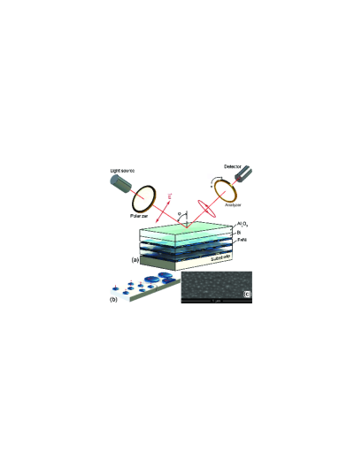
Recently, we have demonstrated that the electronic properties of the free and localized Ta charge carriers in (Ta–FeNi)N multilayer films (MLFs) can be studied by spectroscopic ellipsometry (SE) Kovaleva_APL_2 ; Kovaleva_srep . Here, we explore the elaborated SE approach to gain insights into the electron band structure and surface electronic properties of ultrathin Bi layers in real GMR-type (Bi–FeNi)N MLF structures, incorporating nanoisland FeNi layers (see the scheme of the (Bi–FeNi)N MLFs investigated in the present study by SE in Fig. 1(a)). The morphology and magnetic properties of a single-layer nanoisland FeNi film grown on the Sitall substrate were studied earlier Kovaleva_JNM ; Boltaev ; Kovaleva_JNR . Below the structural percolation transition at the nominal thickness of 1.5 – 1.8 nm Pudonin_JETP , the FeNi layer is discontinuous and consists of inhomogeneously distributed FM nanoislands having lateral sizes of 5 – 30 nm and possessing giant magnetic moments of 103–105 (where is the Bohr magneton). As an example, Fig. 1(c) shows the scanning electron microscopy (SEM) image of the nanoisland FeNi film grown on the Sitall substrate Noskova . As schematically shown in Fig. 1(b), the larger islands (which appear closer to the percolation transition) have the in-plane magnetization configuration, while the smaller islands (existing quite far from the percolation transition) have the out-of-plane one Vedmedenko ; Kovaleva_JNM . Here, collective superferromagnetic (SFM) states – FM or AFM – may develop in the self-assembled local arrangements of FM nanoislands at comparatively high temperatures Kovaleva_JNM ; Kleemann . However, small and well separated FeNi nanoislands are weakly interacting via the magnetic dipole forces and exhibit superparamagnetic (SPM) behavior at high temperatures, which is associated with strongly fluctuating giant magnetic moments Kovaleva_JNM .
The (Bi – FeNi)N MLFs were grown by rf sputtering deposition from 99.95 % pure Bi and Fe21Ni79 targets on glass Sitall (TiO2) substrates. Before the deposition, the vacuum chamber was annealed at 200∘C, so that the prepared base pressure in the chamber was below 2 10-6 Torr. During the deposition, the background Ar pressure was 610-4 Torr. The actual temperature of the substrates was about 80∘C. We used the Sitall substrates with typical sizes of 1550.6 mm3. The Bi and FeNi layer nominal thickness was controlled by the deposition time determined by the film deposition rate. For example, the determined FeNi layer deposition rate was about 0.67 per second. To protect the grown MLFs from the oxidation under ambient conditions, the as deposited MLFs were covered in situ by the 2.1 nm-thick Al2O3 layer. In the prepared (Bi–FeNi)N MLF samples, the FeNi layer nominal thickness was 0.8 and 1.2 nm, the thickness of the Bi layer was 0.6, 1.4, 2.0, and 2.5 nm, and the number of Bi/FeNi bilayers was N = 16. In our recent study, (Ta–FeNi) MLFs grown by rf sputtering deposition onto Sitall-glass substrates, including ultrathin 0.52 nm-thick FeNi layers, were characterized by scanning/transmission electron microscopy (STEM) (for details see Kovaleva_srep ). Here, the grown Bi–FeNi MLF samples were characterized by the atomic-force microscopy (AFM), X-ray diffraction, and X-ray reflectivity (see supplementary material to this article). The X-ray reflectivity measurements confirm a good periodicity and relatively small interface roughness in the grown Bi–FeNi MLF structures, as well as good agreement with the nominal thickness of the Bi and FeNi layers. The X-ray diffraction suggests orientation of the Bi layers along the (012) plane, where the interlayer distance is 3.28 . Thus, the prepared Bi–FeNi MLFs having the Bi layer thickness of 0.6, 1.4, 2.0, and 2.5 nm correspond to about 2, 4, 6, and 8 Bi(012) monolayers.
| FeNi | Bi | |||||
|---|---|---|---|---|---|---|
| (nm) | (nm) | (eV) | (eV) | (eV) | ||
| 2.5 | 254 | 1.40.1 | 9618 | 0.32 | 0.83 | |
| 1.2 | 2.0 | 233 | 2.20.1 | 979 | 0.40 | 1.08 |
| 1.4 | 640.3 | 0.750.17 | 199 | 0.81 | 1.32 | |
| 2.5 | 971 | 0.459 | 1.271 | |||
| 0.8 | 2.0 | 981 | 0.481 | 1.354 | ||
| 1.4 | 1031 | 0.429 | 1.628 |
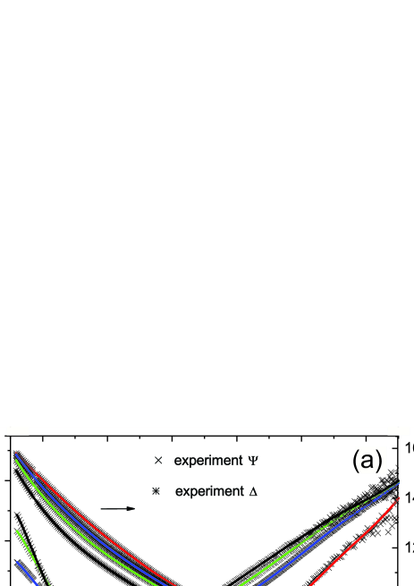
The ellipsometric angles and were measured for the prepared Al2O3/(Bi-FeNi)16/Sitall MLF samples at room temperature at three or four angles of incidence of 60∘, 65∘, 70∘, and 75∘ in a wide photon energy range of 0.5–6.5 eV with a J.A. Woollam VUV-VASE spectroscopic ellipsometer (Fig. 2(a,b) illustrates the and measured at 70∘). The complex dielectric function of each Bi or FeNi layer was modeled by the Drude term and the sum of Lorentz oscillators to account for the contributions of free charge carriers and interband optical transitions, respectively
| (1) |
where is the high frequency dielectric constant. The fitted Drude parameters were (related to the plasma frequency via ) and scattering rate . The adjustable Lorentz oscillator parameters were , , and of the peak energy, full width at half maximum, and peak height, respectively. The ellipsometric angles, and , measured at different angles of incidence were fitted simultaneously in the framework of the multilayer model Al2O3/[Bi(2.5, 2.0, 1.4, 0.6 nm)–FeNi(0.8, 1.2 nm)]16/Sitall, where, in addition, the surface roughness was taken into account by the standard effective medium approximation (EMA) based on the Bruggeman model (50% Al2O3 – 50% vacuum), using the J.A. Woollam VASE software WVASE_software . In the simulation of the ellipsometric angles, and , the Bi layers in each MLF structure were described by the dispersion models (Eq. (1)), including three Lorentz oscillators and the Drude term where necessary. The discontinuous nanoisland FeNi layers were modeled by the effective dielectric function in EMA, which describes the optical properties of a complex composite by an effective homogeneous medium. In the utilized multilayer model, the spectra of the complex dielectric function of the blank Sitall substrate obtained from our previous SE studies Kovaleva_metals ; Kovaleva_APL_1 were substituted. The Bi and FeNi layer thicknesses were fitted to their respective nominal values. The good quality of the fit obtained for the measured angle of incidence of 70∘ is demonstrated by Fig. 2(a,b), where we plot the recorded ellipsometric angles and and the fitting results. The details of the used model and the resulting Drude-Lorentz parameters along with the fit quality check are given in supplementary material to this article. The simulation in the framework of the multilayer model for the Al2O3/(Bi–FeNi)16/Sitall MLFs, where the Bi–FeNi interface roughness is explicitly included, does not essentially improve the fit (see the analysis presented in Kovaleva_APL_2 ), suggesting that the Bi–FeNi interface roughness is essentially incorporated in the EMA dielectric function of the nanoisland FeNi layers.
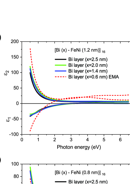
From the multilayer model simulations, the dielectric function spectra of the Bi and FeNi layers were obtained (see supplementary material for details). Here, we are particularly interested in the dielectric function spectra, and , of the Bi layer in the studied [Bi(2.5, 2.0, 1.4, 0.6 nm)–FeNi(1.2 nm)]16 and [Bi(2.5, 2.0, 1.4, 0.6 nm)–FeNi(0.8 nm)]16 MLFs, and the spectra obtained from the best-fit simulations of the and are shown in Fig. 3(a,b). One can notice different trends in the behavior of the corresponding and spectra. Thus, the spectra in Fig. 3(b) exhibit a clearly pronounced minimum at about 0.8 eV, whereas spectra in Fig. 3(a) display more negative values falling down to –50. Accordingly, the spectra in Fig. 3(a) demonstrate a steeper rise at the lowest probed photon energies. Moreover, the dielectric function spectra of the 0.6 nm-thick Bi layers in the studied [Bi(0.6 nm)–FeNi(0.8, 1.2 nm)]16 MLFs display apparent trends toward more pronounced metallic behavior at the lowest probed photon energies, the exhibits a sharp downturn to negative values, and dramatically increases (see Fig. 3(a,b) and supplementary material to this article).
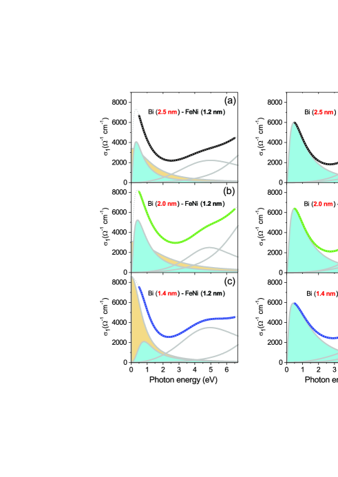
In Fig. 4(a–f) we present the Bi intralayer optical conductivity, [cm-1]/60, in the studied [Bi(2.5, 2.0, 1.4 nm)–FeNi(0.8,1.2 nm)]16 MLFs. Here, the dispersion analysis representation resulting from the multilayer model simulations using Eq. (1) is explicitly demonstrated. On one hand, the simulation results for the three [Bi(2.5, 2.0, 1.4 nm)–FeNi(0.8 nm)]16 MLF structures, including the 0.8 nm-thick nanoisland FeNi layer, indicate that the Bi layer low-energy response is dominated by a pronounced Lorentz band peaking at 0.43 – 0.48 eV having the peak height of 97 – 103 (see Table I). The low-energy interband transition with a high oscillator strength is observed in the dense Bi layers at the energy of 0.8 eV having the peak height of about 120 Hunderi ; Toudert . The low-energy peak at 0.8 eV is also seen in the averaged over anisotropy low-energy dielectric function response of single crystals Wang ; Lenham . This strong low-energy optical transition is associated with interband transitions with the onset near the point, and Golin , and with interband transitions near the T point TT Liu . Therefore, we can conclude that the low-energy optical response of the Bi layer in the [Bi(2.5, 2.0, 1.4 nm)–FeNi(0.8 nm)]16 MLFs (see Fig. 4(d–f)) is dominated by the Bi semimetallic-like electron band structure. On the other hand, our model simulations imply that the optical conductivity of the Bi layer in the [Bi(2.5, 2.0, 1.4 nm)–FeNi(1.2 nm)]16 MLFs, including the 1.2 nm-thick nanoisland FeNi layer, has competing contributions from the low-energy Lorentz band and from the Drude term (see Fig. 4(a–c) and Table I). For the 2.5 and 2.0 nm thick Bi layers, the estimated Drude parameters are similar to those characterizing the surface metallic states arising due to the Rashba effect in ultrathin Bi(001) films Yokota ( = 2300 cm-1 and =2.0 eV). However, it was shown that the surface layer in the ultrathin Bi(012) films can possess a pseudocubic Bi-oriented allotrope with the even number of layers (represented by black phosphorus-like puckered layers) NagaoPRL . We have found that with decreasing the Bi layer thickness from 2.0 to 1.4 nm (corresponding to about six and four Bi(012) monolayers, respectively), the Drude dc limit significantly increases from about 3100400 to 860040 cm-1, and the scattering rate decreases from 2.20.2 to 0.80.2 eV. At the same time, the low-energy Lorentz band becomes significantly suppressed (see Fig. 4(a–c)). The observed evolution of the competing Drude and Lorentz parts can be attributed to the progressive increase in the contribution of the Bi surface metallic states. However, note the difference from the results obtained for the 40–2.8 nm-thick Bi(001) single-layer films Yokota , where the and increase with a decrease of the film thickness. We suppose that here a GMR-like case plays an important role. Indeed, in the GMR-type MLF structures, FM coupling is found for 2.5 nm and 1.3 nm-thick spacer layers, and AFM coupling is found for a 2 nm-thick spacer layer Reiss . The existence of AFM or FM GMR-type correlations between the discontinuous nanoisland FeNi layers could occur in the SFM regime Kovaleva_JNM ; Kleemann ; Kovaleva_JNR . Therefore, in the studied GMR-type [Bi(2.5, 2.0, 1.4 nm)–FeNi(1.2 nm)]16 MLFs, the magnetic interaction between the neighboring FeNi layers, which is responsible for the spin-dependent scattering in the magnetic layer, oscillates from FM via AFM to FM ones. The spin-dependent scattering at the Bi/FeNi interface necessarily affects the scattering of the Bi surface metallic charge carriers (), which should decrease for the FM coupling and increase for the AFM coupling between the neighdoring FeNi layers. The decrease of the of the surface metallic charge carriers in the FM regime will naturally lead to the increase in the optical conductivity limit (see Fig. 4(c)). According to the results of the present multilayer model simulations for the [Bi(2.5, 2.0, 1.4 nm)–FeNi(0.8, nm)]16 MLFs, including the 0.8 nm-thick nanoisland FeNi layers, the Bi layer exhibits semimetallic bulk-like electron band structure, however, the Drude surface metallic conductivity (the Drude term) is implicit in Fig. 4(d–f). Here, with decreasing the FeNi layer thickness, strong SPM-type fluctuations of giant magnetic moments of the FeNi nanoislands become important Kovaleva_JNM ; Kovaleva_JNR . In our recent study Kovaleva_srep , we reported that this leads to localization phenomena in the GMR-type MLFs, introduced by an additional strong magnetic disorder and long-range many-body interactions between giant magnetic moments of FeNi nanoislands. Therefore, the lack of evidence on the surface metallic states for the Bi layer in the [Bi(2.5, 2.0, 1.4 nm)–FeNi(0.8, nm)]16 MLFs can be referred to strong SPM-type fluctuations of giant magnetic moments of FM FeNi nanoislands, leading to strong scattering and localization of scarce free charge carriers in the Bi surface layer. In addition, we found that the dielectric function spectra of the two Bi monolayers demonstrate pronounced metallicity properties in the [Bi(0.6 nm)–FeNi(0.8, 1.2 nm)]16 MLFs. The origin of the discovered semimetal-to-metall crossover needs to be further investigated. In particular, the impact of lattice mismatch at the interface on the electron band structure of 2D bismuthene Liu_RSC and the AFM mechanism of a giant SOC-splitting Rashba1 in the presence of AFM spin textures at the interface should be considered.
In conclusion,
using the advances of the spectroscopic ellipsometry approach,
we extracted the (pseudo)dielectric function spectra
of the ultrathin Bi layers incorporating from two to eight
Bi(012) monolayers in the
[Bi(0.6, 1.4, 2.0, 2.5, nm)–FeNi(0.8, 1.2 nm)]
multilayer structures grown by rf sputtering deposition.
We found that the Bi(012) layers inside
the studied multilayer film structures can possess
the surface metallic conductivity, which is strongly influenced
by the morphology and magnetic properties of the nanoisland
FeNi layer. The obtained results may be useful for implementing
the full potential of the GMR applications based on quasi-2D Bi
layers.
See the supplementary material for the atomic force
microscopy (AFM), X-ray reflectivity (XRR), and X-ray diffraction
(XRD) characterization of the MLFs and for details of the
spectroscopic ellipsometry study.
This work was partially supported by the Czech Science Foundation
(Project No. 20-21864S), and European Structural and Investment Funds
and the Czech Ministry of Education, Youth, and Sports
(Project No. SOLID21, CZ.02.1.01/0.0/0.0/16-019/0000760).
The theoretical analysis performed by K. Kugel was supported by
the Russian Science Foundation, project No. 21-12-0254
(https://rscf.ru/en/project/21-12-00254/).
The authors have no conflicts to disclose.
The data that support the findings of this study are available within this article (and its supplementary material).
References
- (1) Y. A. Bychkov and E. I. Rashba, JETP Lett. 39, 78 (1984).
- (2) M.-Y. Liu, Y. Huang, Q.-Y. Chen, Z.-Y. Li, C. Cao, and Y. He, RSC Adv. 7, 39546 (2017).
- (3) X. Gonze, J.-P. Michenaud, and J.-P. Vigneron, Phys. Rev. B 41, 11827 (1990).
- (4) C. A. Hoffman, J. R. Meyer, F. J. Bartoli, A. Di Venere, X. J. Yi, C. L. Hou, H. C. Wang, J. B. Ketterson, and G. K. Wong, Phys. Rev. B 48, 11431 (1993).
- (5) J. Toudert, R. Serna, I. Camps, J. Wojcik, P. Mascher, E. Rebollar, and T. A. Ezquerra, J. Phys. Chem. C 121, 3511 (2017).
- (6) K. Yokota, J. Takeda, C. Dang, G. Han, D. N. McCarthy, T. Nagao, S. Hishita, K. Kitajima, and I. Katayama, Appl. Phys. Lett. 100, 251605 (2012).
- (7) N. N. Kovaleva, D. Chvostova, O. Pacherova, L. Fekete, K. I. Kugel, F. A. Pudonin, and A. Dejneka, Appl. Phys. Lett. 111, 183104 (2017).
- (8) N. N. Kovaleva, F. V. Kusmartsev, A. B. Mekhiya, I. N. Trunkin, D. Chvostova, A. B. Davydov, L. N. Oveshnikov, O. Pacherova, I. A. Sherstnev, A. Kusmartseva, K. I. Kugel, A. Dejneka, F. A. Pudonin, Y. Luo, and B. A. Aronzon, Sci. Rep. 10, 21172 (2020).
- (9) A. Stupakov, A. V. Bagdinov, V. V. Prokhorov, A. N. Bagdinova, E. I. Demikhov, A. Dejneka, K. I. Kugel, A. A. Gorbatsevich, F. A. Pudonin, and N. N. Kovaleva, J. Nanomater., 3190260 (2016).
- (10) A. P. Boltaev, F. A. Pudonin, I. A. Sherstnev, and D. A. Egorov, J. Phys. Condens. Matter 30, 295804 (2018).
- (11) N. N. Kovaleva, A. V. Bagdinov, A. Stupakov, A. Dejneka, E. I. Demikhov, A. A. Gorbatsevich, F. A. Pudonin, K. I. Kugel, and F. V. Kusmartsev, J. Nanopart. Res. 20, 109 (2018).
- (12) A. P. Boltaev, F. A. Pudonin, I. A. Sherstnev, and D. A. Egorov, J. Exp. Theor. Phys. 125, 465 (2017).
- (13) D. D. Noskova, F. A. Pudonin, I. A. Sherstnev, G. N. Eroshenko, D. A. Egorov, and A. M. Shadrin, Phys. Lett. A 410, 127546 (2021).
- (14) E. Y. Vedmedenko, H. P. Oepen, and J. Kirschner, Phys. Rev. B 67, 012409 (2003).
- (15) W. Kleemann, O. Petracic, Ch. Binek, G. N. Kakazei, Yu. G. Pogorelov, J. B. Sousa, S. Cardoso, and P. P. Freitas, Phys. Rev. B 63, 134423 (2001).
- (16) J.A. Woollam VASE Spectroscopic Ellipsometry Data Analysis Software. (J.A. Woollam Co.: Lincoln, NE, USA, 2010).
- (17) N. Kovaleva, D. Chvostova, and A. Dejneka, Metals 7, 257 (2017).
- (18) N. N. Kovaleva, D. Chvostova, A. V. Bagdinov, M. G. Petrova, E. I. Demikhov, F. A. Pudonin, and A. Dejneka, Appl. Phys. Lett. 106, 051907 (2015).
- (19) O. Hunderi, J. Phys. F 5, 2214 (1975).
- (20) J. Toudert and R. Serna, Opt. Mater. Express 7, 2299 (2017).
- (21) P. Y. Wang and A. L. Jain, Phys. Rev. B 2, 2978 (1970).
- (22) A. P. Lenham, D. M. Treherne, and R. J. Metcalfe, J. Opt. Soc. Am. 55, 1072 (1965).
- (23) S. Golin, Phys. Rev. B 166, 643 (1968).
- (24) Y. Liu and R. Allen, Phys. Rev. B 52, 1566 (1995).
- (25) T. Nagao, J. T. Sadowski, M. Saito, S. Yaginuma, Y. Fujikawa, T. Kogure, T. Ohno, Y. Hasegawa, S. Hasegawa, and T. Sakurai, Phys. Rev. Lett. 93, 105501 (2004).
- (26) A, Hütten, S. Mrozek, S. Heitmann, T. Hempel, H. Brückl, and G. Reiss, Acta Mater. 47, 4245 (1999).
- (27) L.-D. Yuan, Z. Wang, J.-W. Luo, E. I. Rashba, and A. Zunger, Phys. Rev. B 102, 014422 (2020).