Correlative mapping of local hysteresis properties in VO2
Abstract
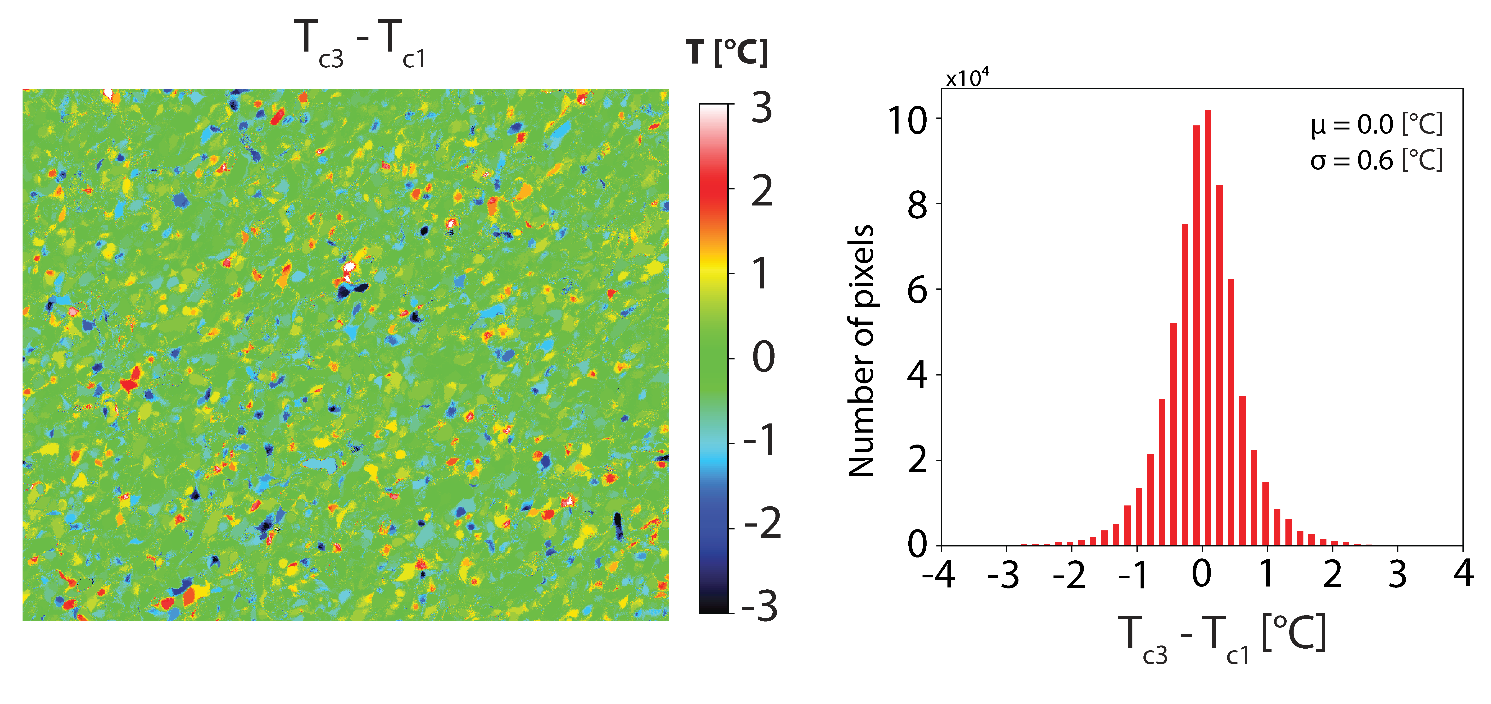
We have developed a new optical microscopy technique able to track micron-sized surface clusters as temperature is varied. Potential candidates for study include phase separated metal-insulator materials, ferroelectrics, and porous structures. Several key techniques (including autofocus, step motor/cross correlation alignments, single-pixel thresholding, pair connectivity correlation length and image convolution) were implemented in order to obtain a time series of thresholded images. Here, we apply this new method to probe the archetypal phase separated insulator-metal transition in VO2. A precise time and temperature series of the insulator-metal transition was achieved, allowing us to construct for the first time in this material spatial maps of the transition temperature Tc. These maps reveal the formation of micron-sized patterns that are reproducible through multiple temperature sweeps within 0.6°C, although a few isolated patches showed Tc deviations up to ±2°C. We also derive maps of the local hysteresis widths Tc and local transition widths Tc. The hysteresis width maps show an average width of Tc =4.3°C, consistent with macroscopic transport measurements, with, however, small regions as low as Tc[0°C-1°C], and as high as 8°C. The transition width Tc maps shows an average of 2.8°C and vary greatly (from 0°C to 8°C), confirming the strong inhomogeneities of Tc in the subpixel structure. A positive correlation between Tc value and hysteresis width Tc is observed by comparing the spatial distributions of each map. Finally, individual pixels with unique transition characteristics are identified and put forward. This unprecedented knowledge of the local properties of each spot along with the behavior of the entire network paves the way to novel electronics applications enabled by, e.g., addressing specific regions with desired memory and/or switching characteristics, as well as detailed explorations of open questions in the theory of hysteresis.
I Introduction
Electronic phase separation commonly emerges in a wide variety of quantum materials such as high-Tc superconductors McElroy et al. (2005), colossal magnetoresistance manganites Fäth et al. (1999), insulator-metal transition (IMT) materials Post et al. (2018), multilayer rhombohedral graphene Shi et al. (2020),etc. An archetypal example of a phase-separated material is vanadium dioxide, VO2, which undergoes a 1st order IMT at Tc 68°C Morin (1959) (i.e., just above room temperature) accompanied by an abrupt several-order-of-magnitude resistivity decrease and monoclinic-to-tetragonal structural change. The exact nature of the transition, whether it is a Peierls transition driven by electron-phonon interactions or a Mott-Hubbard transition driven by electron-electron interactions, is still under debate Tomczak and Biermann (2009). In the vicinity of the transition, VO2 exhibits a spatial coexistence of metal and insulator domains that form intricate patterns Qazilbash et al. (2007). Analyzing the shape, characteristic size and scaling properties of those patterns can yield valuable information about the fundamental interactions that drive the transition Liu et al. (2016a). Therefore, understanding and controlling the phase-separate state in quantum materials has become a major research field in recent years Coll et al. (2019).
Currently, phase separation imaging in quantum materials reported in the literature mostly comes from scanning probe techniques such as STM Fäth et al. (1999); McElroy et al. (2005) and s-SNIM Qazilbash et al. (2007); Liu et al. (2016a). While these methods have a very high spatial resolution, fine temporal resolution remains hard to implement since scanning probes are very time-consuming. Moreover, STM lacks resolution at room temperature and loses registry as the temperature is changed Gomes et al. (2007). To solve this we have developed a new microscopy method to map out clear and stabilized images of the IMT. This optical method allows the precise filming of the transition with hundreds or even thousands of images taken in quick succession ( seconds per final image). This allows us to not only follow fine details in the time evolution of the metal-insulating patches but also to filter out thermal noise if needed. We first describe the sample preparation and optical response. We then describe the experimental steps necessary to achieve this mapping. While most steps are straightforward, four new crucial steps were keys to this study: “Height z focusing”, “Single pixel time traces”, “Pair connectivity correlation length” and “Time domain convolution”. These technical developments allowed us to acquire accurate spatial maps of transition temperature distribution, from which the phase separation patterns can be easily obtained at any given temperature. The Tc maps reveal multiple interesting features including the presence of spots with an extremely large or nearly absent hysteresis of the IMT, a positive correlation between the Tc value and the hysteresis width, and high cycle-to-cycle reproducibility of the transition. The detailed knowledge of local properties is the necessary ingredient to develop and test basic phase separation and hysteresis theories, as well as to gain microscopic understanding of the device performance for practical applications of quantum materials.
II Methods
II.1 VO2 thin film epitaxy, resistivity, and reflectivity
Vanadium dioxide thin films were prepared by reactive RF magnetron sputtering of a V2O3 target (>99.7%, ACI Alloys, Inc.) on an r-cut sapphire substrate. Sample A is 130 thick and sample B is 300 thick. A mixture of ultrahigh purity (UHP) argon and UHP oxygen was used for sputtering. The total pressure during deposition was 4mTorr, and the oxygen partial pressure was optimized to 0.1mTorr (2.5% of the total pressure). The substrate temperature during deposition was 600oC while the RF magnetron power was kept at 100W. Grain size in these films is typically found to be 40-130 in 100-150 films Ramírez et al. (2009). Grain size is expected to typically be slightly larger in the 300 film. The sample is found to have a relative 27% optical change in the visible range when passing the IMT (see SI Sec.S1 for details). Gold electrodes were deposited on top of the film, separated by 10 (sample A) and 30 (sample B). Both samples showed a clear IMT (see Fig. S1) above 68oC as evidenced by a drop in resistivity of 4 orders of magnitude Zimmers et al. (2013).
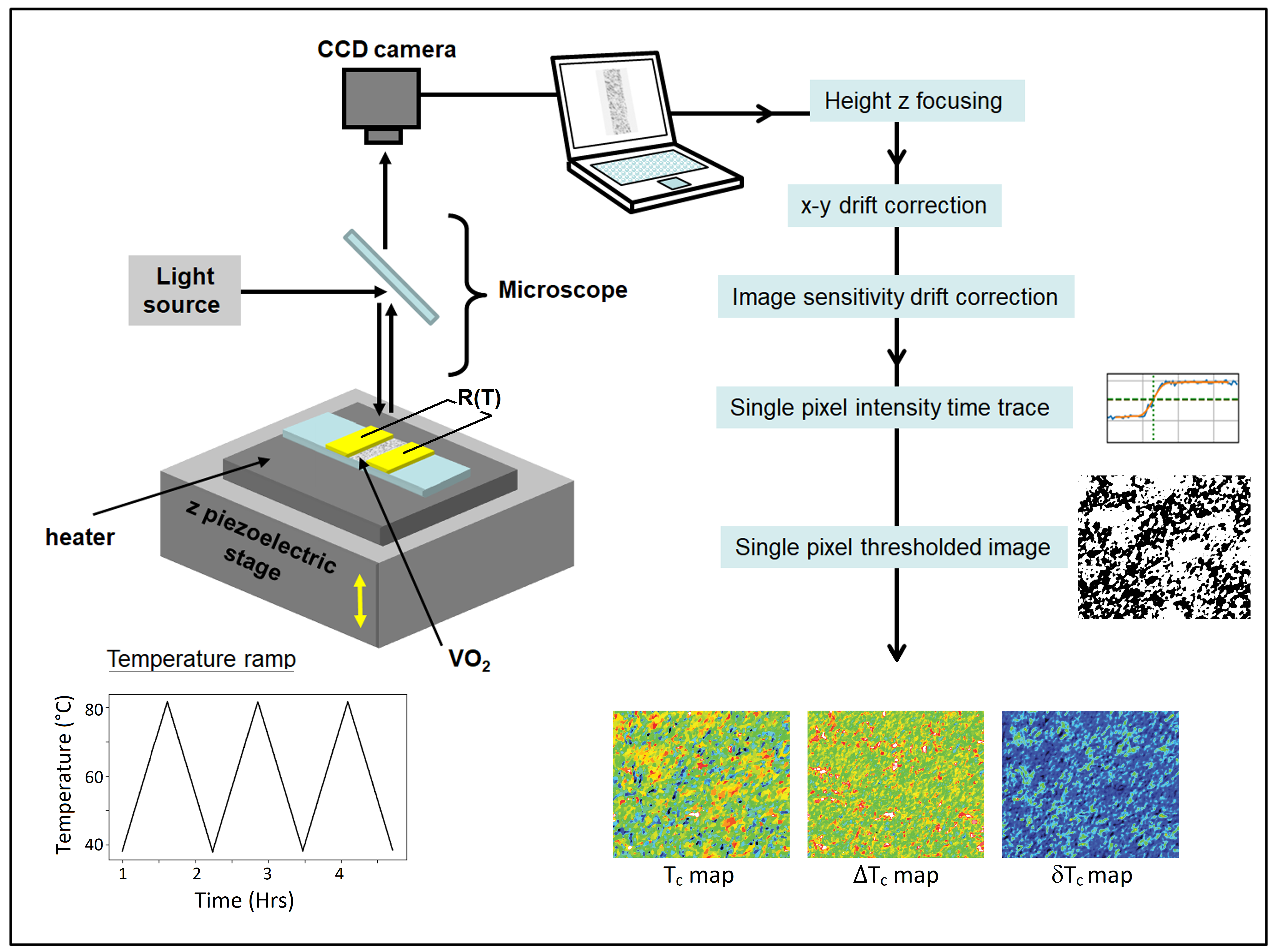
II.2 Image/temperature recording
The optical experimental setup consists of a VO2 thin film sample placed on a Peltier heater or a Linkam Thms350V temperature controller inside a Nikon optical microscope in epi configuration (both the illumination and reflection of light travel through the same objective). Illumination in the visible range was used (halogen lamp, no filters) Currie et al. (2017). Two surface sample images (sample A 1050 and sample B 3035) were measured around the focal point of 1mm in the visible range using a 150 magnification dry Olympus objective lens with an optical aperture of NA = 0.9. The theoretical lateral resolution is estimated to be r= 1.22/(2 NA) = 370 in the visible range using the Rayleigh criterion Mic . Temperature was measured using a Pt100 glued next to the sample. Temperature sweeps (35oCTc to 82oCTc and back) spanning the entire IMT were performed multiple times at a rate of 1°C/min, temperature swept linearly, with temperature and images recorded every 0.17°C.
II.3 Height z focusing and x-y drift correction
Inevitable temperature dilation of the experimental system during temperature sweeps brings the sample out of focus during temperature sweeps. In order to compensate for this z drift, we employ a “fuzzy focusing” technique as follows. During the experiment, the sample was continually moved up and down 10 every 10 seconds by a piezoelectric crystal placed under it, in order to bring the sample in and out of focus. A stack of 120 images was recorded this way for each temperature. Over the years, various metrics have been evaluated for selecting the sharpest image in such a stack Liu et al. (2007); Mir et al. (2014); Pertuz et al. (2013). Some studies focus explicitly on images that don’t have sharp contrast Liu et al. (2016b), like the raw images acquired here (see Fig. 2(m)). Most metrics reported perform well in selecting the focused image. We have first chosen one using the compression rate of the recorded images Edgett et al. (2012). This one is based on the intuitive idea that, when very out of focus, the sample surface will look homogeneously gray due to blurring. In this case, the raw recorded Bitmap (BMP) image can be highly compressed in lossless Tiff format using a standard Lempel-Ziv-Welch (LZW) compression protocol Ziv and Lempel (1978); Welch (1984), since nearly every pixel is the same. On the contrary, when the sample is in focus, the image contains much more information (since most pixels are different from their neighbors), and the raw BMP image cannot be compressed as much. Using this method, one can determine the most sharply focused image in the stack by selecting the one with the largest Tiff file size Not ; PNG . Among the 62,000 images of sample A acquired during the 14 hour experiment (consisting of 3 major temperature loops and 10 subloops Basak et al. (2023)), we retain the 894 images that are in focus within 80.
A recent update of the microscope has allowed us to select the best focused image of sample B the experiment. In the live selection process we have used a computationally faster method based on image gradient using the Tenengrad function Liu et al. (2016b). Both metrics cited above were vetted using micron-sized gold disks lithographed on a glass substrate where the sharpest image can be defined as the image with the sharpest step function (gold to substrate). Using the focusing stack technique, we have also compared the image height on the sample four corners. This allowed us to correct the tilt of the sample (due to sample positioning using thermal paste). The updated setup also uses a piezoelectric PI Pifoc PD72Z1x to move the objective up and down rather than moving the sample placed inside the Linkam stage. The current setup can thus output an image every 10s in focus on the full field of view as a function of temperature.
As the temperature is cycled repeatedly, in addition to drifts along z-axis (perpendicular to the film), there are also drifts in the plane (the plane of the film). These thermal drifts were compensated: () live within 1 using step motors below the sample and () post experiment using cross correlation to track and realign part of the gold leads which contain imperfections (spots) and rough edges with VO2 (see Fig. 5 (a)). Although the lateral image resolution is limited by diffraction and is estimated to be 370nm, the drift compensation tracks each pixel ( 37 wide) on the sample throughout the whole experiment.
The remaining spatial variations we observe in reflected intensity from the VO2 region are primarily due to changes in local reflectivity due to the IMT. However, there can be other contributions to this spatial variation, including effects such as surface height variations from sample warping, variations in film thickness, minor surface defects, and even shadows cast from the 150 thick gold leads. There can even be differences in pixel sensitivity in the camera itself. Because each of these contributions is independent of temperature (i.e. constant in time), their effects can be distinguished from that of the temperature driven IMT, as described in the next section.
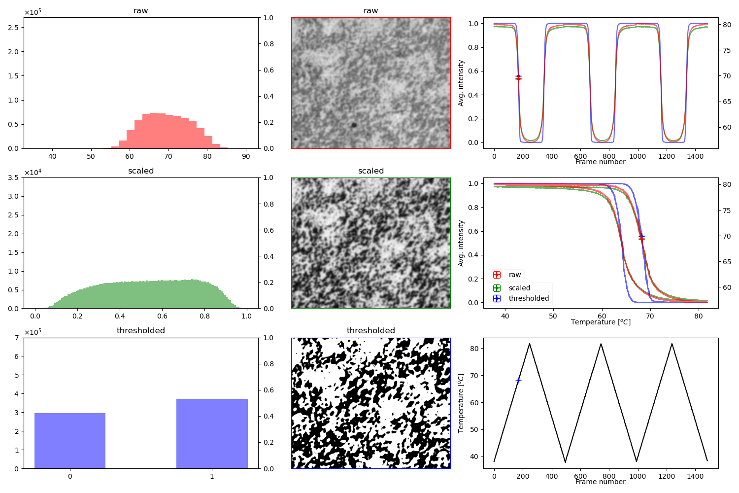
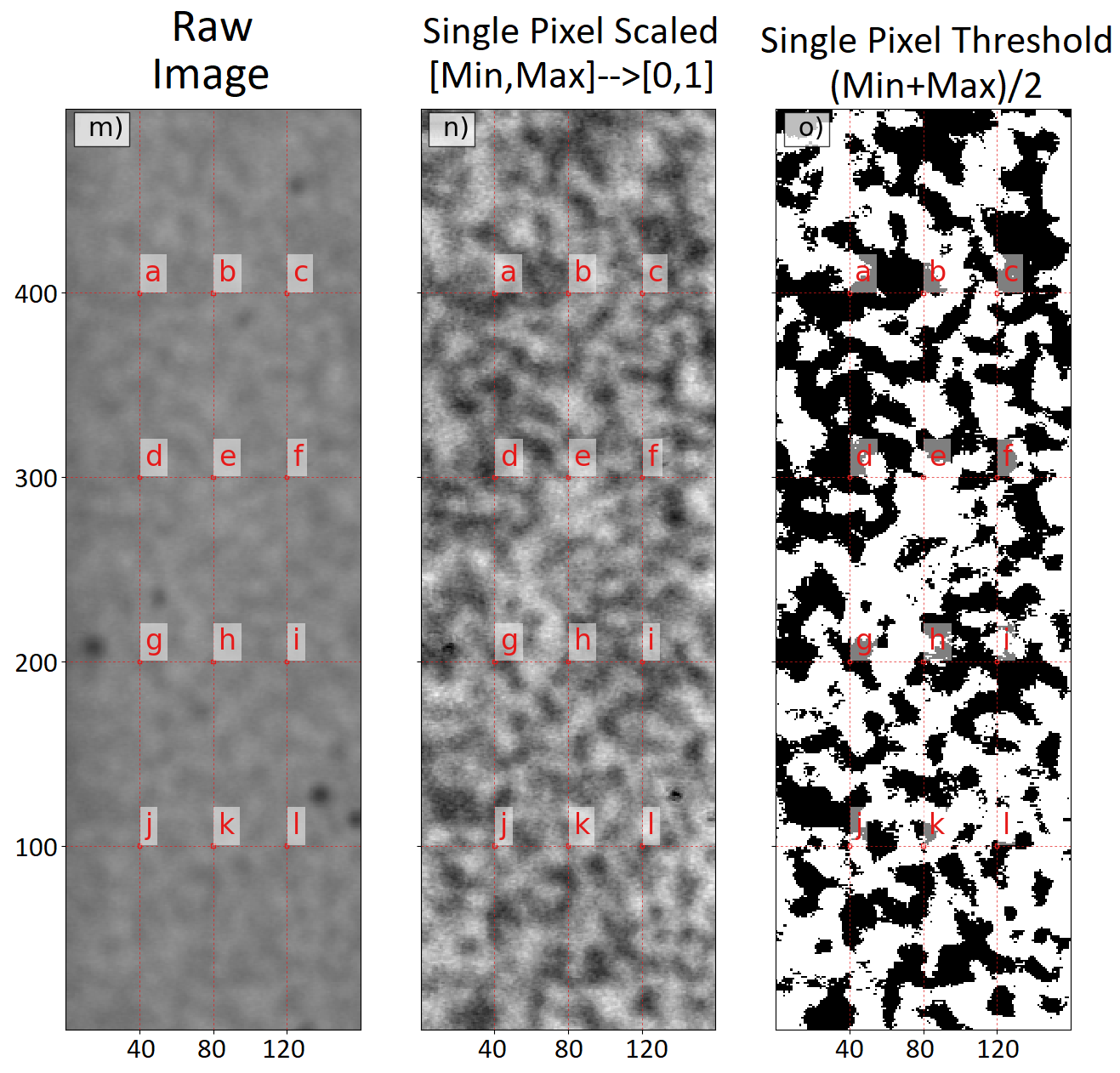
II.4 Single pixel scaled and binary thresholded images
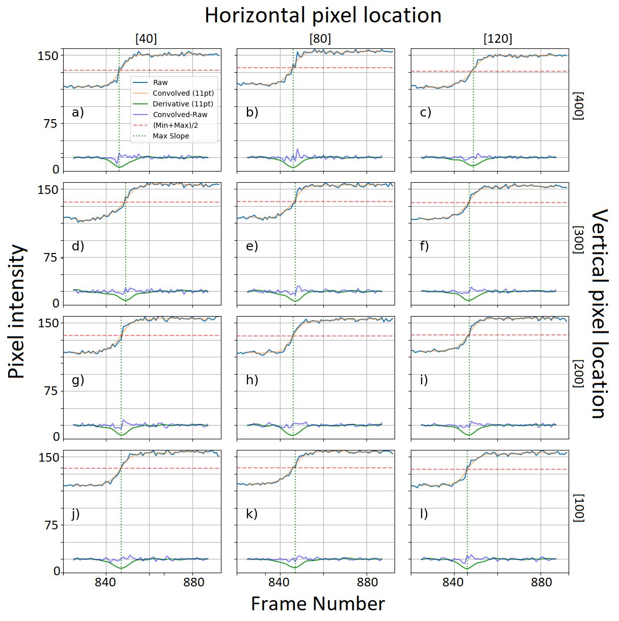
In order to isolate the changes in local reflectivity which are due to the IMT, we introduce two novel image processing techniques. We use single pixel time traces to generate single pixel scaled images (panel (n) of Fig. 2), as well as binary thresholded images (panel (o) of Fig. 2, discussed in the following subsections). Both types of images begin by considering a full warming or cooling sweep (i.e. from fully insulating to fully metallic, or vice versa) to follow the intensity and analyze each pixel individually. As an example, Fig. 2 (a-l) shows the raw optical intensity time/frame traces of 12 different pixels during a cooling sweep. See S6 for the time traces of 1600 pixels from the center of the sample. In order to construct a single pixel scaled image, we normalize each individual pixel’s 8-bit grayscale intensity time trace with respect to itself, such that its maximum intensity is scaled to 1, and its minimum intensity is scaled to 0. The resulting single pixel scaled image is shown in Fig. 2(n). This type of image is a relatively quick way to study the temperature dependent IMT, as it eliminates temperature-independent spatial variations that are not due to the IMT.
In order to construct a binary thresholded image which clearly delineates metal and insulator domains, we must define a criterion for when each pixel changes from metal to insulator or vice versa. The orange curve in each of the panels (a-l) in Fig. 2 is a Gaussian-smoothed version of the raw time trace, using an 11-point Gaussian convolution (=2.5). We use this smoothed time trace of the intensity in order to determine the midway point intensity for each individual pixel (shown by the red horizontal dotted lines). We use the pair connectivity correlation length to justify setting the threshold at midway, as described in the following subsections (Secs. II.4.1 and II.4.2). This allows us to construct binary black and white images of the metal and insulator domains at each measured temperature, as shown in Fig. 2(o). Different pixels go through the midway point at different frame numbers, and therefore at different temperatures. We use this information to construct spatial maps of the local transition temperature Tc recorded at each pixel revealing the highly spatially-textured nature of the IMT in VO2 Qazilbash et al. (2007); Liu et al. (2016a). These Tc maps, as well as hysteresis width Tc maps and transition width Tc maps, are presented in the experimental results Sec. III.
II.4.1 Pair Connectivity Correlation Length
As can be seen in the single pixel time traces shown in Fig. 2 (see SI Figures. S6 for many more examples), each pixel experiences a definite switch from metal to insulator or vice versa, consistent with the Ising-type model we have previously developed to describe the IMT in VO2 thin films Liu et al. (2016a); Basak et al. (2022). While the Ising model was originally developed to describe magnetic domains of orientation “up” or “down”, here we map “up” and “down” to metal and insulator domains. While the metal-insulator transition is first order, this transition ends in a critical point as a function of quenched disorder. The influence of that critical point is felt throughout a critical region, which includes part of the first order line in the vicinity of the critical end point.Liu et al. (2016a) We use the correlation length of the pair connectivity correlation function to determine the threshold between metal and insulator domains. During the IMT, VO2 metal-insulator domains form intricate patterns, often becoming fractal due to proximity to a critical point Liu et al. (2016a). At criticality, correlation lengths diverge. Away from criticality, the divergence is muted, although the correlation length still displays a maximum at the point of closest approach to criticality. For example, changing the interaction strength between metal and insulator domains to be farther away from criticality, or changing the strength of various types of disorder farther from criticality causes the correlation length to go down. Similarly, changing the intensity threshold by which we identify metal and insulator domains also changes this correlation length. In disordered systems, setting an unphysical threshold will not move the system toward criticality, but only away. Therefore, one way to set the proper threshold between metal and insulator domains is to maximize the correlation length.
The pair connectivity correlation function is familiar from percolation models, where the corresponding pair connectivity correlation length diverges at the critical point Stauffer and Aharony (2018). Coniglio and coworkers showed that the pair connectivity correlation length also diverges at the critical temperature in the two-dimensional Ising model Coniglio et al. (1977). We have recently shown that the pair connectivity correlation length also diverges at other Ising critical points, including that of the two-dimensional random field Ising model Song et al. (2021), as well as on slices of three dimensional models at criticality, including the clean Ising model Liu et al. (2021) and the random field Ising model Song et al. (2021). Near a critical point, the correlation function is power law at distances less than the correlation length, in this case . This pair correlation length can be calculated directly from an image via Coniglio and Fierro (2009):
| (1) |
where is the likelihood that i and j are in the same finite cluster. Another way to view this is as:
| (2) |
where is the radius of gyration of each connected cluster, and the average is taken over the finite clusters. This quantity diverges at the percolation threshold as:
| (3) |
It diverges at clean Ising transitions as:
| (4) |
and it diverges at random field Ising transitions as:
| (5) |
II.4.2 Setting Thresholds of Metal and Insulator Signal in Optical Data
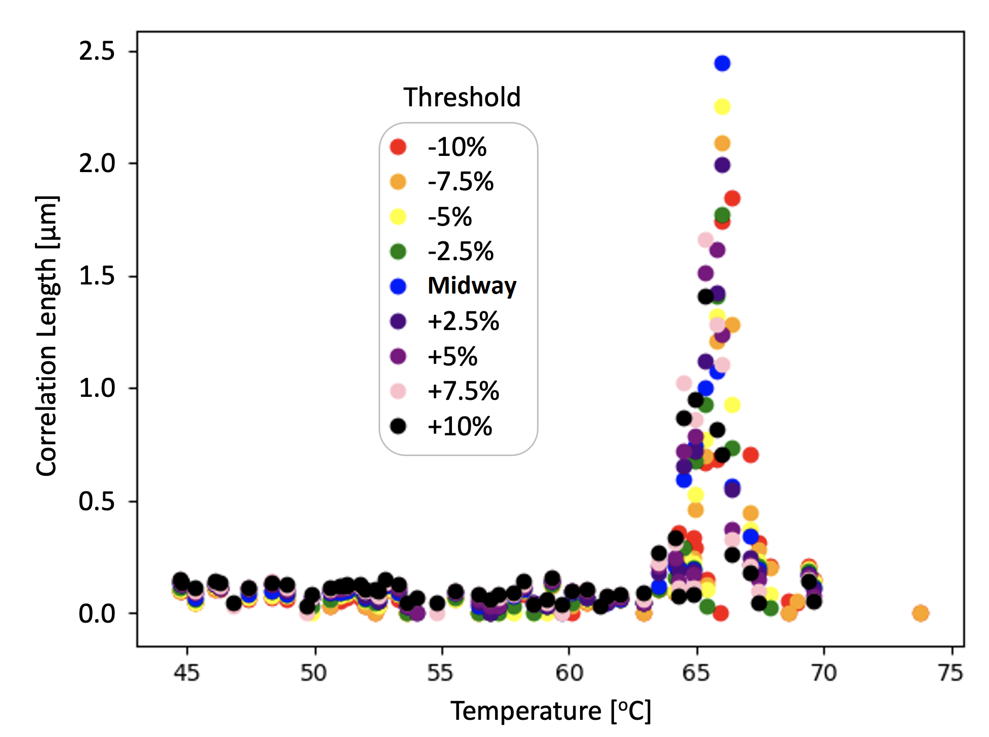
In order to know at what intensity to set the threshold between metal and insulator in each pixel, we calculate the pair connectivity correlation length in a series of images, as a function of different intensity thresholds. For this we use the single pixel scaled images as described in the previous subsection. In Fig. 3, we plot the evolution of the pair connectivity correlation length (Eqn. 1) during the warming branch of a hysteresis loop. The blue circles in Fig. 3 have each pixel’s threshold set at the midway point of that particular pixel’s intensity. The black circles have each pixel’s threshold set higher by an amount that is of the difference between the saturated metal and saturated insulator values of intensity. The pink circles have each pixel’s threshold set higher by only , and similarly for other colors as denoted in the figure legend. Similar to the way the theoretical threshold was set in Ref. Liu et al. (2016a), we set the threshold according to the longest correlation lengths. Since in Fig. 3 the longest correlation length happens for a threshold equal to the average between metal and insulator intensity (the blue circles in Fig. 3) we use this midway threshold throughout the paper.
II.5 Time domain convolution
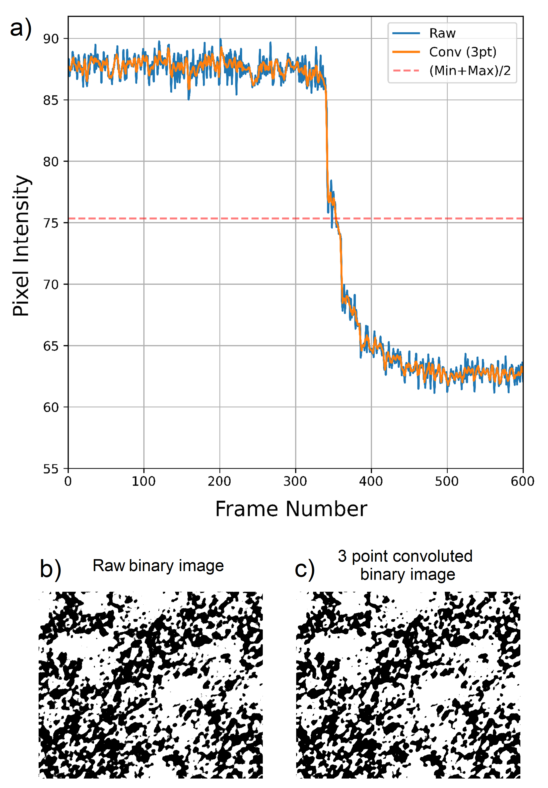
One of the strong points of obtaining a series of 100-1000 images via this autofocus optical microscope is the possibility of filtering out high frequency noise. A similar technique is used in resistivity experiments that probe samples thousands of times per second. Fig. 4 (a) compares a raw single pixel time trace to a smoothed version in which a 3-point Gaussian convolution (=2.5) has been applied in the time domain. In this example, the raw single pixel time trace crosses the midway point twice, whereas the 3-point convolved curve passes the midway point only once. Notice that this procedure of filtering high frequency noise in the time domain greatly suppresses the white noise evident in the spatial domain near the metal-insulator boundaries derived from the raw time traces (see Fig. 4 (b) and (c) for comparison). This smoothing is useful for studying spatial correlations from frame to frame. However, if filtering is not necessary, raw data is used throughout the analysis. This is the case for Tc maps in the section below and ramp reversal memory maps presented elsewhere Basak et al. (2023). High frequency noise was filtered in the temperature data taken using the Pt100 by fitting a linear slope through the large temperature sweeps. This matched the internal temperature sensor slope of the Linkam Thms350V temperature controller.
III Results
Having described the various key steps in the previous sections (including autofocusing, step motor/cross correlation aligning, single pixel scaling and thresholding, pair connectivity correlation length analysis, and time domain convolution) we now present the detailed spatially-resolved study of the IMT in VO2 films using our new optical mapping method.
Maps
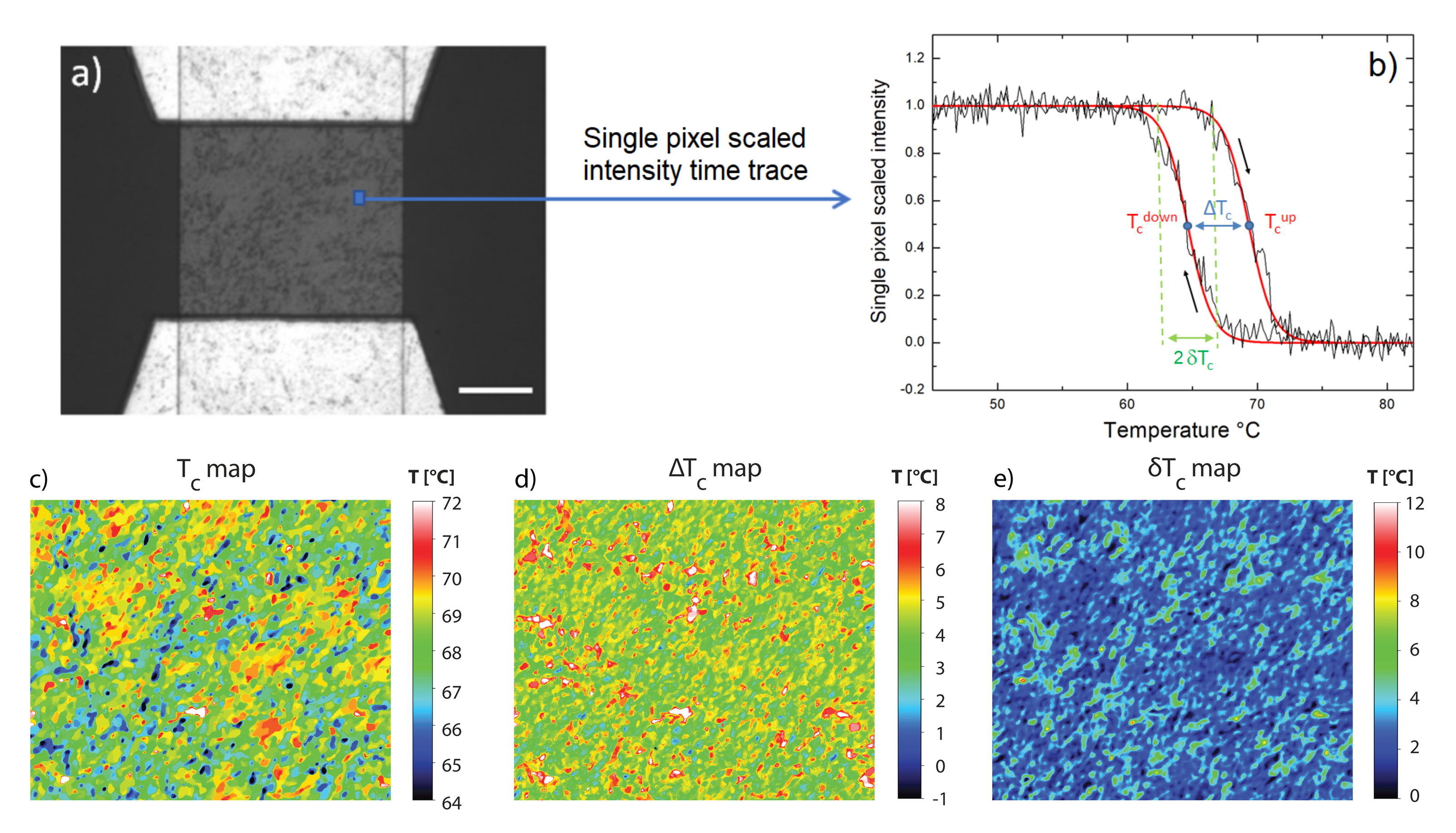
Transition Temperature Tc maps: Fig. 5 (c) reports the local critical temperature Tc map in VO2 sample B. These maps show a large spatial variation in Tc, with rich pattern formation over tens of microns, similar to s-SNIM sub-micron measurements Qazilbash et al. (2007), but acquired with a much faster procedure that allows for much finer time and temperature resolution. This large scale spatial variation, along with detailed spatial knowledge of the location of these variations, can potentially be exploited to optimize memory elements by addressing specific regions of the sample.
Reproducibility of Tc maps: Previous reports on avalanches in this material showed jumps in resistivity randomly appearing during the transition in macroscopic transport measurements Sharoni et al. (2008). This suggested that the metal-insulator patterns could be appearing randomly during each temperature sweep. At first glance, this appears to be at odds with the optical data reported in this study, where we find that the metal and insulator patterns are highly repeatable globally (occurring at the same location and with the same shape) during successive temperature sweeps (see Fig 6). The repeatability suggests that the patterns are strongly influenced by an underlying random field present in the thin film or its substrate Liu et al. (2016a); Burzawa et al. (2019); Basak et al. (2022). The observed stochasticity of resistance jumps in transport measurements Sharoni et al. (2008) could arise from small variations in the exact time at which avalanches are triggered. In addition, small changes in optical maps can potentially create large changes in resistance, when tiny “shorts” connect pre-existing larger metallic clusters.
Transition Width Tc maps: The transition width Tc of each pixel can be accessed by fitting single pixel scaled intensity time traces to a hyperbolic tangent: ()-1). Because Tc is known from our time trace analysis, there is only one fitting parameter. The map of Tc distribution is shown in Fig. 5 (e). The average transition width of the pixels as measured in optics is °C with extremes from 0°C to 8°C. Moreover, a small number of pixels show more than one step during a transition (see for example first pixel (305,300) in Fig. S6). These cases could arise from an overlap between multiple metal or insulator domains affecting a single pixel. This could be due to information from surrounding pixels affecting the signal at one pixel, since the pixel size is 10 times smaller than the resolution. Or, it could arise from structures that are smaller than the pixel size. Indeed, s-SNIM has clearly observed inhomogeneities on smaller length scales than the optical maps presented here Qazilbash et al. (2007); Liu et al. (2016a). Interestingly, the standard deviation of local Tc’s across the sample, (1.2°C), is smaller than the average transition width of pixels Tc(2.8°C). It remains an open question whether the self-similar metal-insulator domain patterns discussed in Ref. Liu et al. (2016a) could be the source of this difference.
Hysteresis Width Tc maps: By subtracting Tcup-Tcdown (see the caption of Fig.5 (b) for the definition) one can construct a hysteresis width Tc map. The hysteresis width Tc map is shown in Fig. 5 (d) for sample B. The average width is found to be °C as seen in macroscopic transport measurements. However, certain small regions have small Tc, in the range [0°C - 1°C] (small blue clusters in Fig. 5 (d)). Probing these region with other local probes could shed light on whether this is an intrinsic property of these regions. These hysteresis-free patches could be very useful in multiple switching applications such as optical electronic devices. Indeed it has been shown that the presence of a large hysteresis in VO2 greatly complicates using it as an optical sensor Gurvitch et al. (2009).
Correlations between maps
With all of the maps above, one can check for correlations between these quantities. Fig. 8 plots Tc vs. , vs. and Tc vs. for each pixel. A few horizontal and diagonal lines appear in these plots. The horizontal lines come from multiple pixels (spatially close by) switching at the same temperature (upon warming). The diagonal lines come from multiple pixels (spatially close by) switching at the same temperature (upon cooling). Although this is typically what one would expect from avalanches, further analysis is needed to extract the full dynamics occurring. In the three correlation maps, no trend is seen in the last two, but Tc vs. shows a slight positive correlation. This means that pixels with low Tc tend to have low (i.e. close to zero) and vice versa. The positive correlation in Fig. 8(a) is not to be confused with the few diagonal lines present in this panel explained just above.
Hand picking specific hysteric properties
The wide range of behaviors contained in the three maps presented in the section above (Fig. 5 c, d and e), gives us the unprecedented opportunity to find individual pixels with desired properties. Fig. 9 shows the Tc map of the sample with six different types of pixels selected. The pixel labeled “std” for standard has a rounded transition with values of Tc, Tc and Tc which are close to the average values found in the distribution of these three quantities (see Fig. 7 a, b and c).
Pixels A and B show the most common type of local characteristics found in the maps: when Tc is high, Tc is high; when Tc is low, Tc is low. This positive correlation is evident at a global level in Fig. 8 (a). However, on a local level, individual pixels can have a large deviation from the global average behavior. Indeed pixel E shows a possibility of finding Tc very low (0.3°C) with a Tc (66.3°C) low but closer to the mean value of the map.
Pixels C and D illustrate the case where the width Tc of the transition is very sharp (0.5°C) or very wide (5°C). Pixel C shows a representative sharp pixel, where within the temperature steps of 0.17°C, the transition occurs in a sharp, avalanche mode. Further analysis to see where and how these avalanches occur will be pursued in future work.
Finally pixel E shows a case where Tc is within the lower values [0°C-1°C]. As mentioned previously, small hysteresis could be useful in opto-electronic devices or neuromorphic devices. In the first case, small hysteresis avoids optical detectors getting stuck in subloops Gurvitch et al. (2009); in the second case, small hysteresis allows lowering the voltage threshold needed for spiking Maffezzoni et al. (2015).
General remarks on the pixel selection procedure: () as mentioned previously in the section above, some pixels in the map clearly present two steps during the IMT. These two-step pixels can potentially be detected in an automated way from their anomalously high error on the fit to the hyperbolic tangent function; () the features put forward in these 6 pixels above are not unique to the 37 square pixel location. These features usually also hold for many pixels around the coordinates reported.
IV Conclusions
We have reported the first Tc maps derived from single pixel optical imaging on VO2. Multiple new experimental steps were needed to align, focus and calibrate the raw grayscale images recorded. These experimental achievements allowed us to accurately track the spatial distribution of metal and insulator clusters. Binary black and white images, time traces, Tc maps, Tc maps, and Tc maps were plotted and discussed. The sample shows micron-sized patterns that are found to be mostly reproducible through multiple temperature sweeps. The hysteresis width map exhibits, on average, the same average hysteresis width of 4.3°C as macroscopic resistivity hysteresis, but exhibits strong variation on a local scale, down to [0°C-1°C] in certain small regions and as large as 8°C in other regions. These findings open an exciting opportunity to access local properties of VO2 by, e.g., contacting specific parts of the sample electrically in order to select unique parameter combinations for specific applications in electrical and optoelectronic devices. The observation of a positive correlation between Tc value and hysteresis width could enable a new approach for tailoring the material’s response to external drives, in addition to providing a new perspective in studying open questions in the theory of hysteresis.
Acknowledgements
We thank M. J. Carlson for technical assistance with image stabilization, and acknowledge helpful conversations with K. A. Dahmen. S.B., F.S., and E.W.C. acknowledge support from NSF Grant No. DMR-2006192 and the Research Corporation for Science Advancement Cottrell SEED Award. S.B. acknowledges support from a Bilsland Dissertation Fellowship. E.W.C. acknowledges support from a Fulbright Fellowship, and thanks the Laboratoire de Physique et d’Étude des Matériaux (LPEM) at École Supérieure de Physique et de Chimie Industrielles de la Ville de Paris (ESPCI) for hospitality. This research was supported in part through computational resources provided by Research Computing at Purdue, West Lafayette, Indiana rca . The work at UCSD (PS, IKS) was supported by the Air Force Office of Scientific Research under award number FA9550-20-1-0242. The work at ESPCI (M.A.B., L.A., and A.Z.) was supported by Cofund AI4theSciences hosted by PSL University, through the European Union’s Horizon 2020 Research and Innovation Programme under the Marie Skłodowska-Curie Grant No. 945304.
References
- McElroy et al. (2005) K. McElroy, J. Lee, J. A. Slezak, D.-H. Lee, H. Eisaki, S. Uchida, and J. C. Davis, Science 309, 1048 (2005).
- Fäth et al. (1999) M. Fäth, S. Freisem, A. A. Menovsky, Y. Tomioka, J. Aarts, and J. A. Mydosh, Science 285, 1540 (1999).
- Post et al. (2018) K. W. Post, A. S. McLeod, M. Hepting, M. Bluschke, Y. Wang, G. Cristiani, G. Logvenov, A. Charnukha, G. X. Ni, P. Radhakrishnan, M. Minola, A. Pasupathy, A. V. Boris, E. Benckiser, K. A. Dahmen, E. W. Carlson, B. Keimer, and D. N. Basov, Nature Physics 14, 1056 (2018).
- Shi et al. (2020) Y. Shi, S. Xu, Y. Yang, S. Slizovskiy, S. V. Morozov, S.-K. Son, S. Ozdemir, C. Mullan, J. Barrier, J. Yin, A. I. Berdyugin, B. A. Piot, T. Taniguchi, K. Watanabe, V. I. Fal’ko, K. S. Novoselov, A. K. Geim, and A. Mishchenko, Nature 584, 210 (2020).
- Morin (1959) F. J. Morin, Physical Review Letters 3, 34 (1959).
- Tomczak and Biermann (2009) J. M. Tomczak and S. Biermann, Physical Review B 80 (2009).
- Qazilbash et al. (2007) M. M. Qazilbash, M. Brehm, B.-G. Chae, P.-C. Ho, G. O. Andreev, B.-J. Kim, S. J. Yun, A. V. Balatsky, M. B. Maple, F. Keilmann, H.-T. Kim, and D. N. Basov, Science 318, 1750 (2007).
- Liu et al. (2016a) S. Liu, B. Phillabaum, E. W. Carlson, K. A. Dahmen, N. S. Vidhyadhiraja, M. M. Qazilbash, and D. N. Basov, Phys. Rev. Lett. 116, 036401 (2016a).
- Coll et al. (2019) M. Coll, J. Fontcuberta, M. Althammer, M. Bibes, H. Boschker, A. Calleja, G. Cheng, M. Cuoco, R. Dittmann, B. Dkhil, I. E. Baggari, M. Fanciulli, I. Fina, E. Fortunato, C. Frontera, S. Fujita, V. Garcia, S. Goennenwein, C.-G. Granqvist, J. Grollier, R. Gross, A. Hagfeldt, G. Herranz, K. Hono, E. Houwman, M. Huijben, A. Kalaboukhov, D. Keeble, G. Koster, L. Kourkoutis, J. Levy, M. Lira-Cantu, J. MacManus-Driscoll, J. Mannhart, R. Martins, S. Menzel, T. Mikolajick, M. Napari, M. Nguyen, G. Niklasson, C. Paillard, S. Panigrahi, G. Rijnders, F. Sánchez, P. Sanchis, S. Sanna, D. Schlom, U. Schroeder, K. Shen, A. Siemon, M. Spreitzer, H. Sukegawa, R. Tamayo, J. van den Brink, N. Pryds, and F. M. Granozio, Applied Surface Science 482, 1 (2019).
- Gomes et al. (2007) K. K. Gomes, A. N. Pasupathy, A. Pushp, S. Ono, Y. Ando, and A. Yazdani, Nature 447, 569 (2007).
- Ramírez et al. (2009) J.-G. Ramírez, A. Sharoni, Y. Dubi, M. E. Gómez, and I. K. Schuller, Physical Review B 79, 235110 (2009).
- Zimmers et al. (2013) A. Zimmers, L. Aigouy, M. Mortier, A. Sharoni, S. Wang, K. G. West, J. G. Ramirez, and I. K. Schuller, Physical Review Letters 110, 056601 (2013).
- Currie et al. (2017) M. Currie, M. A. Mastro, and V. D. Wheeler, Optical Materials Express 7, 1697 (2017).
- (14) Wikipedia on microscope resolution; https://en.wikipedia.org/wiki/Angular_resolution.
- (15) C. R. Taylor, Finite Difference Coefficients Calculator, https://web.media.mit.edu/~crtaylor/calculator.html.
- Liu et al. (2007) X. Y. Liu, W. H. Wang, and Y. Sun, Journal of Microscopy 227, 15 (2007).
- Mir et al. (2014) H. Mir, P. Xu, and P. van Beek, in Proc. SPIE, Vol. 9023, edited by N. Sampat, R. Tezaur, S. Battiato, and B. A. Fowler (SPIE, 2014) p. 90230I.
- Pertuz et al. (2013) S. Pertuz, D. Puig, and M. A. Garcia, Pattern Recognition 46, 1415 (2013).
- Liu et al. (2016b) S. Liu, M. Liu, and Z. Yang, EURASIP Journal on Advances in Signal Processing 2016, 70 (2016b).
- Edgett et al. (2012) K. S. Edgett, R. A. Yingst, M. A. Ravine, M. A. Caplinger, J. N. Maki, F. T. Ghaemi, J. A. Schaffner, J. F. Bell, L. J. Edwards, K. E. Herkenhoff, E. Heydari, L. C. Kah, M. T. Lemmon, M. E. Minitti, T. S. Olson, T. J. Parker, S. K. Rowland, J. Schieber, R. J. Sullivan, D. Y. Sumner, P. C. Thomas, E. H. Jensen, J. J. Simmonds, A. J. Sengstacken, R. G. Willson, and W. Goetz, Space Science Reviews 170, 259 (2012).
- Ziv and Lempel (1978) J. Ziv and A. Lempel, IEEE Transactions on Information Theory 24, 530 (1978).
- Welch (1984) T. A. Welch, Computer 17, 8 (1984).
- (23) One should note that using lossless PNG format as the final compressed format generates issues as it has a black and white filter.PNG This generates the unfortunate consequence of creating an unequal file size for simple white vs. a simple black image of the same number of pixels.
- (24) Compression algorithms comparison, https://cloudinary.com/blog/a_one_color_image_is_worth_ two_thousand_words.
- Basak et al. (2023) S. Basak, Y. Sun, M. Alzate Banguero, F. Simmons, P. Salev, I. K. Schuller, L. Aigouy, E. W. Carlson, and A. Zimmers, submitted (2023).
- Basak et al. (2022) S. Basak, M. Alzate Banguero, L. Burzawa, F. Simmons, P. Salev, L. Aigouy, M. M. Qazilbash, I. K. Schuller, D. N. Basov, A. Zimmers, and Carlson, arXiv (2022), 2211.01490 .
- Stauffer and Aharony (2018) D. Stauffer and A. Aharony, Introduction To Percolation Theory (Taylor & Francis, 2018).
- Coniglio et al. (1977) A. Coniglio, C. R. Nappi, F. Peruggi, and L. Russo, Journal of Physics A: Mathematical and General 10, 205 (1977).
- Song et al. (2021) C.-L. Song, E. J. Main, F. Simmons, S. Liu, B. Phillabaum, K. A. Dahmen, E. W. Hudson, J. E. Hoffman, and E. W. Carlson, arXiv (2021), 2111.05389 .
- Liu et al. (2021) S. Liu, E. W. Carlson, and K. A. Dahmen, Condensed Matter 6, 39 (2021).
- Coniglio and Fierro (2009) A. Coniglio and A. Fierro, Encyclopedia of Complexity and Systems Science , p.1596 (2009).
- (32) Online movie: MIT in VO2; www.youtube.com/watch?v=XoXQKpnjn7o.
- Sharoni et al. (2008) A. Sharoni, J. G. Ramirez, and I. K. Schuller, Physical Review Letters 101, 026404 (2008).
- Burzawa et al. (2019) L. Burzawa, S. Liu, and E. W. Carlson, Phys. Rev. Materials 3, 033805 (2019).
- Gurvitch et al. (2009) M. Gurvitch, S. Luryi, A. Polyakov, and A. Shabalov, Journal of Applied Physics 106, 104504 (2009).
- Maffezzoni et al. (2015) P. Maffezzoni, L. Daniel, N. Shukla, S. Datta, and A. Raychowdhury, IEEE Transactions on Circuits and Systems I: Regular Papers 62, 2207 (2015).
-
(37)
G. McCartney, T. Hacker and B. Yang,
Educause Review, 2014; https://er.educause.edu/articles/2014/7/
empowering-faculty-a-campus-cyberinfrastructure-strategy-for-research-communities. - Qazilbash et al. (2008) M. M. Qazilbash, A. A. Schafgans, K. S. Burch, S. J. Yun, B. G. Chae, B. J. Kim, H. T. Kim, and D. N. Basov, Physical Review B 77, 115121 (2008).
- Zimmers et al. (2005) A. Zimmers, J. M. Tomczak, R. P. S. M. Lobo, N. Bontemps, C. P. Hill, M. C. Barr, Y. Dagan, R. L. Greene, A. J. Millis, and C. C. Homes, Europhysics Letters (EPL) 70, 225 (2005).
Supporting Information: Correlative mapping of local hysteresis properties in VO2
S1 VO2 Reflectivity
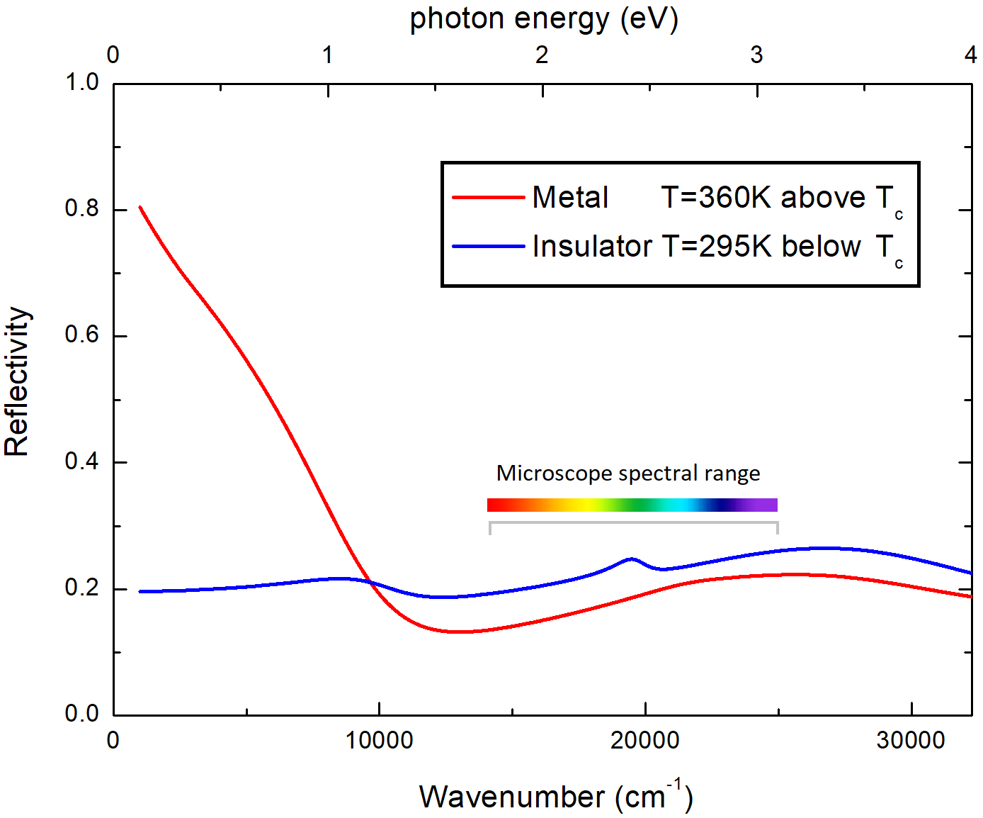
The fact that the metallic reflectivity of VO2 is lower than that of the insulating phase in the visible range is counterintuitive.
This is due to a subtle combination of a Drude response as well as intraband and interband transitions and thin film interferences in this material.
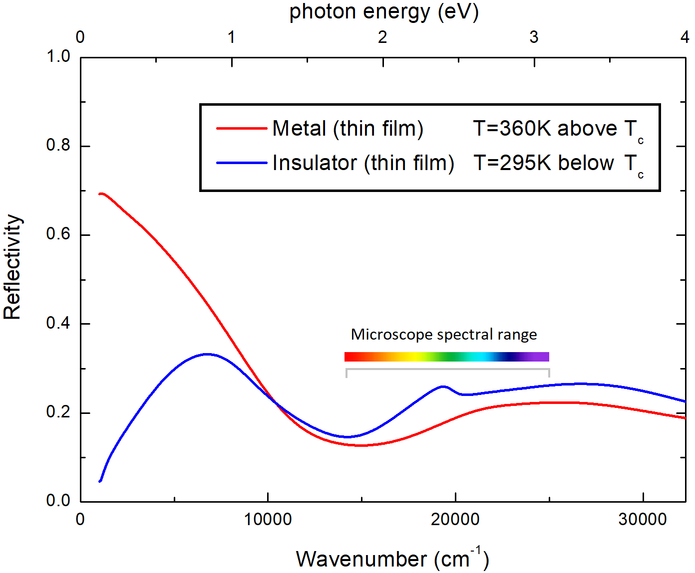
The largest reported spectra in VO2 was measured by ellipsometry Qazilbash et al. (2008). Using the reported real part of the optical conductivity , we have calculated the reflectivity of the insulator and metallic states (see Fig. S2 and S3). This clearly shows that, as one would expect in the infrared, the sample becomes highly reflective when metallic. Above the plasma frequency (12000), interband transitions and spectral weight conservation make the reflectivity curves cross, leading to the metallic state having a lower reflectivity than the insulating state in this range. The relative optical contrast in the visible range (27%), is still more than sufficient in our setup to identify both states clearly (as seen in a raw image Fig. S1 (a)).
S2 Key steps making this study possible
The key step that have allowed us completing this study comes from the unique qualities of the VO2 material :
- The IMT is above room temperature, which allows close optical microscopy (strong objective 150 with a high numerical aperture 0.9 brought to 1 focus above the sample surface). This setup would be much harder to achieve if cryogenic cooling (i.e. a cryostat with a window between the sample and objective) was needed.
- Phase separation was observed by s-SNIM at sub-micron scales in this material Qazilbash et al. (2007); Liu et al. (2016a). The fact that this phase separation is still found up to 30 makes these optical microscopy surface maps possible.
- In the visible range, a relative 27% drop in the thin film reflectivity is found in the metallic state Measuring in the visible range gave us results with a 400 resolution. In the infrared, the contrast between metal and insulator is much larger, as expected, but only allows optical resolution up to the IR wavelength, i.e. 1-10.
S3 Image sensitivity drift correction
Whereas the relative average intensity of VO2 increases almost 30% in changing from metal to insulator, the change in sapphire reflectance in this temperature range is negligible. We have used this fact to correct for any changes in incident light or CCD detector sensitivity throughout the experiment by dividing the average intensity in the VO2 region by the intensity in the sapphire region of the sample.
Details: We assume that the input intensity is a function of time but spatially uniform. The reflected intensity from any region is . Since the Sapphire’s reflectance does not vary significantly over the range of temperature the sample went through, it is assumed to be a constant. Let the spatially averaged sapphire reflectivity be . Then, the spatial average reflected intensity from the sapphire region is: Any region of VO2 has a reflected intensity: . Therefore, the ratio of reflected intensities from Sapphire and VO2 is independent of input intensity: . We will use as a reference to correct for any variation due to fluctuation of ambient light. The quantity independent of input intensity: , Hence, setting the reference input intensity , the corrected reflected intensity from VO2 would be:
S4 Single pixel thresholded images: inflection point
In the main text, we have set the threshold between metal and insulator domains at the midway point of the intensity, based on the pair connectivity correlation length criterion described in Sec. II.4.
We also tested another method of setting the threshold based on
the inflection point of the single pixel time traces.
The green curves in panels (a-l) of Fig. 2 show a smoothed derivative of the raw time traces, achieved by using a finite difference with a 11-point Gaussian convolution (=2.5) fin . The vertical dotted green line shows the extremum of this derivative, which locates the inflection point of the orange curves. Since the pixel switching curves (orange and blue traces) exhibit a relatively rapid change from metal to insulator, this inflection point at which the pixel brightness is changing most rapidly is the most natural place to assign a change from insulator to metal and vice versa. Because we have used a stencil with even number of 10, the inflection point happens between frames, and allows us to clearly identify frames which precede the inflection point (which are metallic) from frames which come after the inflection point (which are insulating).
Notice that the frame number at which the solid orange curves cross the dotted orange lines coincides with the inflection point for each pixel. This means that both methods are equivalent for determining the frame number at which a pixel switches from metal to insulator or vice versa.