External screening and lifetime of exciton population in single-layer ReSe2 probed by time- and angle-resolved photoemission spectroscopy
Abstract
The semiconductor ReSe2 is characterized by a strongly anisotropic optical absorption and is therefore promising as an optically active component in two-dimensional heterostructures. However, the underlying femtosecond dynamics of photoinduced excitations in such materials has not been sufficiently explored. Here, we apply an infrared optical excitation to single-layer ReSe2 grown on a bilayer graphene substrate and monitor the temporal evolution of the excited state signal using time- and angle-resolved photoemission spectroscopy. We measure an optical gap of eV, consistent with resonant excitation of the lowest exciton state. The exciton distribution is tunable via the linear polarization of the pump pulse and exhibits a biexponential decay with time constants given by fs and fs, facilitated by recombination via an in-gap state that is pinned at the Fermi level. By extracting the momentum-resolved exciton distribution we estimate its real-space radial extent to be greater than 17.1 Å, implying significant exciton delocalization due to screening from the bilayer graphene substrate.
Among the semiconducting transition metal dichalcogenides (TMDCs), rhenium-based compounds such as ReSe2 are distinctive due to their anisotropic 1T′ structure, resulting from an in-plane Jahn-Teller-like distortion Kertesz and Hoffmann (1984). The lattice structure can be thought of as one-dimensional chains of Re atoms, reducing the three-fold symmetry of a common equilateral hexagonal lattice that describes most other semiconducting TMDCs Manzeli et al. (2017). The reduced symmetry introduces a linear anisotropy for optical absorption Zhong et al. (2015). Consequently, ReSe2 stands out as a potential candidate material for multifunctional two-dimensional optoelectronic devices, such as photodetectors Zhang et al. (2016); Afzal et al. (2021); Li et al. (2022) and field effect transistors Yang et al. (2014); Corbet et al. (2016); Pradhan et al. (2018); Rehman et al. (2021).
The electronic structure of ReSe2 exhibits a direct quasiparticle gap at the -point of the Brillouin zone (BZ), which has been calculated to be 1.49 eV in the bulk and 2.44 eV in a free-standing single layer (SL) Arora et al. (2017). Scanning tunneling spectroscopy (STS) measurements of SL ReSe2 have shown a gap of 1.7 eV when the material is supported on bilayer graphene on silicon carbide Choi et al. (2020); Thi Ly et al. (2022) and 2.0 eV when supported on graphene on hexagonal boron nitride Qiu et al. (2019). This variation in gap sizes underscores the important role of substrate screening. Photoluminescence measurements have revealed an optical gap of 1.39 eV in thick films that increases to 1.51 eV in SL ReSe2, corresponding to the lowest exciton transition in the system Arora et al. (2017); Kipczak et al. (2020); Wolverson et al. (2014); Zhao et al. (2015).
The dynamics of photoinduced carriers has been investigated in multilayer and bulk ReSe2 via pump-probe measurements of the differential transmissivity at pump wavelengths of 400 and 800 nm, revealing biexponential decay dynamics on timescales of 10 ps and 80 ps caused by the interplay of exciton formation and decay with hot carrier generation and relaxation Liu et al. (2019); He et al. (2018). In exfoliated SL ReSe2 on insulating subtrates the differential transmittivity exhibits dynamics on the order of 10 ps He et al. (2018). Integration of SL ReSe2 with SL MoS2 in a vertical heterostructure enables further tuning of photoinduced carrier lifetimes via the formation of interlayer excitons with relaxation time constants exceeding 300 ps Yang et al. (2021).
Further insights to the light-matter interaction in SL ReSe2 are required in order to design optoelectronic devices. Indeed, the ultrafast dynamics and excitonic properties of SL ReSe2 in the presence of conductive graphene layers has not been studied.
Here, we use time- and angle-resolved photoemission spectroscopy (TR-ARPES) in order to determine the ultrafast dynamics of excitons in SL ReSe2 epitaxially grown on electron-doped bilayer graphene. By applying an 800 nm optical excitation, we observe a significant population of both exciton and in-gap states, with a strong dependence of the exciton signal on the polarisation of the pump pulse. The exciton population exhibits an ultrafast biexponential decay with time constants of fs and fs. Our momentum-resolved measurements of the exciton distribution lead to a lower estimate of the exciton radius of 17.1 Å on bilayer graphene, indicating that the substrate screening causes a relatively high degree of exciton delocalization compared to bulk ReSe2, where the radius is 9.6 Å Arora et al. (2017).
SL ReSe2 is grown using molecular beam expitaxy on a 6H-SiC substrate, which is annealed at 1573 K to form a bilayer of graphene via thermal decomposition of SiC. Re and Se atoms are co-evaporated from an e-beam evaporator and an effusion cell, respectively, at a sample temperature of 523 K for 10 min. Following annealing at 693 K for 30 min, a 0.8 ML ReSe2 layer is formed with three-fold rotated domains, as described in detail in Ref. Choi et al. (2020). The bilayer graphene is substantially electron-doped with a carrier concentration of 1.6 1013 cm-2 Choi et al. (2020). The sample is encapsulated in a thick layer of Se to avoid contamination during transfer through air to the photoemission experiment.
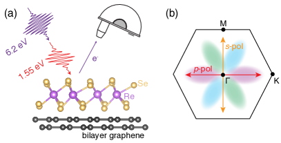
The TR-ARPES measurements are performed at the T-ReX facility in Trieste, Italy. Equilibrium ARPES measurements of the valence band (VB) are performed using the ninth harmonic at 10.8 eV of a Yb fiber laser Peli et al. (2020). For time-resolved measurements, a 250 kHz Ti:sapphire laser with a fundamental energy of 1.55 eV is split in two time-delayed pulses with the fundamental beam applied as a pump pulse and the other part used as a probe pulse at 6.2 eV via generation of the fourth harmonic. The probe pulses are always -polarized. Photoemitted electrons are detected using a SPECS Phoibos 225 analyser. An overview of the experiment is presented schematically in Fig. 1(a). The time, energy and angular resolution are set to 150 fs, 50 meV and 0.2∘, respectively. The Se capping layer on the ReSe2 sample is removed via one hour of annealing to a sample temperature of 473 K prior to TR-ARPES measurements. The sample is kept at 120 K throughout the measurements unless stated otherwise.
The linear polarisation of the pump pulse is varied between and via a half-wave plate. ReSe2 has largest optical oscillator strength along the direction for the exciton at , corresponding to a -polarized pump pulse in our geometry as shown in Fig. 1(b) Zhong et al. (2015); Zhao et al. (2015). In a single-orientation crystal, the oscillator strength is expected to be suppressed for an -polarised pump pulse, which is oriented along for our geometry. However, our SL ReSe2 grows in 120∘-rotated domains such that the difference between the three non-equivalent high symmetry points at the BZ corners of the native 1T′ structure is lost and a peak in oscillator strength occurs along each direction, as shown in Fig. 1(b) via pink, blue and green ovals.
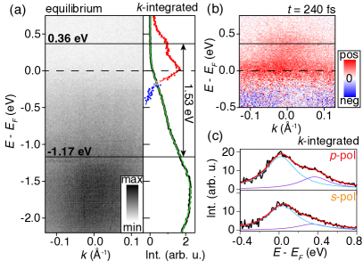
An equilibrium ARPES spectrum of SL ReSe2 around the VB maximum at , acquired with the 10.8 eV probe pulse, is shown in Fig. 2(a). The left panel presents the -dependent ARPES intensity while the right panel shows the corresponding energy distribution curve (EDC) integrated over from -0.05 to 0.05 Å-1. From the Fermi level (see dashed horizontal line) and towards lower energies the intensity of the background increases monotonically until a broad peak of intensity is reached. The onset of this broad peak is determined by fitting the -integrated EDC with a double exponential rise function, allowing to discriminate between the rise in background intensity and the rise in intensity caused by the ReSe2 VB. The VB offset determined via this method is eV, which is in good agreement with the value of -1.1 eV obtained for a similar sample measured in a synchrotron-based ARPES experiment Choi et al. (2020). The broad and relatively featureless VB dispersion within the narrow -window we can access with a 10.8 eV probe pulse is consistent with previous experiments and emerges from a manifold of states with a high photoemission cross section in our measurement geometry Choi et al. (2020). The background intensity is attributed to in-gap states, which have been observed in STS measurements on SL ReSe2 supported on bilayer graphene, and are caused by a distribution of trapped charge impurities at the van der Waals interface between ReSe2 and bilayer graphene Thi Ly et al. (2022).
The response of SL ReSe2 to optical excitation with a 1.55 eV -polarised pump pulse is presented in Fig. 2(b) via the -dependent intensity difference determined by subtracting a spectrum acquired before optical excitation () from a spectrum measured around the peak of the optical excitation at fs. The excited state is probed using a photon energy of 6.2 eV, precluding access to excited holes in the VB due to the low photoelectron kinetic energies that can be reached. An increase of photoemission intensity due to excitation (red contrast in Fig 2(b)) is observed across the full -range around and in a region centred at higher energy and localized in around . Extracting an EDC of the intensity difference integrated over from -0.05 to 0.05 Å-1 and fitting with two Lorentzian peaks on a linear background reveals the lower excitation is centred at (0.02 0.01) eV and the higher at (0.36 0.01) eV, as shown in Fig. 2(a). The lower excitation is consistent with a charge impurity-induced in-gap state pinned at due to the lack of dispersion and complete delocalization in Ulstrup et al. (2016); Majchrzak et al. (2021).
A gap of eV is determined between the VB offset and the higher excitation, as seen via double-headed arrows in Fig. 2(a). This value is substantially lower than the quasiparticle bandgap of 1.7 eV measured by STS on SL ReSe2 on bilayer graphene Choi et al. (2020); Thi Ly et al. (2022). Strikingly, the energy coincides with the lower exciton line in SL ReSe2 supported on insulating substrates measured by photoluminescence Arora et al. (2017); Kipczak et al. (2020), leading to the conclusion that we observe the optical gap and that the exciton is resonantly excited by the infrared pump pulse in our experiment. The exciton binding energy and quasiparticle gap may vary depending on how the Coulomb interaction is screened by the substrate and by excited charge carriers but the optical gap remains fixed Qiu et al. (2019).
Changing the pump pulse polarisation from to causes a notable decrease of intensity from the exciton state relative to the in-gap state as shown via the -integrated EDCs around the peak of excitation obtained with the two polarisations in Fig. 2(c). The spectral weight is extracted as the area of Lorentzian profiles fitted to the EDCs (see blue and purple curves in Fig. 2(c)), revealing a 34 % reduction of the exciton intensity relative to the in-gap state intensity in the case of -polarisation. This reduction is consistent with the expected anisotropy of the exciton Zhong et al. (2015), as indicated by the pink ovals in Fig. 1(b).
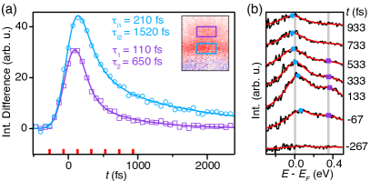
The temporal evolution of the exciton and in-gap state is extracted by integrating the intensity difference over corresponding -regions, as shown in the inset in Fig. 3(a). The resulting traces are shown as purple squares and blue circles in Fig. 3(a), respectively, together with fits to a biexponential decay multiplied by a step function and convoluted with a Gaussian that accounts for the time-resolution. These fits provide time constants for the decay of the exciton state given by fs and fs and for the in-gap state given by fs and fs. The timescales of the exciton signal are significantly shorter than 10 ps and 80 ps reported for SL ReSe2 on an insulating substrate and bulk ReSe2 Liu et al. (2019); He et al. (2018). Here, the similar decay constants for the exciton and in-gap states suggests a strong interplay between ultrafast exciton decay and electron-hole recombination via the in-gap state, possibly also involving the bilayer graphene substrate where similar dynamics may be expected Ulstrup et al. (2014). The slower compared to is indicative of re-filling of the in-gap state via decay of the exciton, underscoring the important role of impurity-induced in-gap states for exciton dynamics Wang et al. (2015a, b).
We inspect how the EDC peak positions of the signals evolve with time in Fig. 3(b). The exciton peak remains fixed for all time-delays where we could reliably fit a Lorentzian function, which further supports our assignment of this feature in terms of the optical gap and not the quasiparticle gap. The latter would be expected to renormalize as a function of time due to the decaying photoinduced carrier density Chernikov et al. (2015); Ulstrup et al. (2016), thereby leading to a time-dependent peak position. The in-gap state exhibits a peak shift towards due to the decrease in Fermi level broadening as the excited carriers cool down.
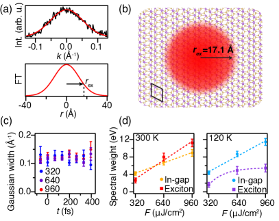
The momentum distribution of the exciton signal measured by TR-ARPES can be related to the spatial distribution of the exciton wavefunction Dong et al. (2021); Man et al. (2021). It is thereby possible to determine how localized or delocalized the exciton is in our SL ReSe2/bilayer graphene heterostructure. The photoemission intensity is proportional to the square of the transition matrix element given by , where is the vector potential, is the momentum operator and () is the final (initial) state of the photoelectron. The final state can be approximated as a plane wave such that the matrix element becomes proportional to the Fourier transform of the initial state wavefunction, , where is the wave vector and signifies a plane wave final state Moser (2017); Dong et al. (2021).
We utilize this relation by integrating the momentum distribution curve (MDC) of the photoemission intensity over an energy range from 0.19 eV to 0.53 eV, which contains the exciton signal. Fitting the MDC to a Gaussian function with a width of 0.07 Å-1 provides the momentum distribution of the exciton. This is Fourier transformed to yield the real-space distribution with a half-width at half maximum (radius) given by Å, as shown in Fig. 4(a). This should be considered a lower estimate due to momentum-broadening factors such as the finite experimental resolution. The size of the exciton is compared with the SL ReSe2 lattice in Fig. 4(b) and is substantially larger than 9.6 Å determined for bulk ReSe2 Arora et al. (2017). External screening caused by the bilayer graphene substrate leads to delocalization of the exciton in real space and thereby the larger radius for our SL ReSe2 Stier et al. (2016). Additionally, by measuring the MDC width for different exciton densities, achieved by varying the pump fluence and time delay, we find the width is insensitive to the density within the error bars of our analysis, as shown in Fig. 4(c). The external screening thereby fully specifies the size of the exciton in our sample.
The spectral weight of the exciton and in-gap states provides a direct measure of their density following optical excitation with different fluence. In Fig. 4(d) we have extracted the spectral weight as the area of Lorentzian fits to EDCs at the peak of excitation, following the approach presented in Fig. 2(c). The analysis is performed for three different settings of fluence and at sample temperatures of 120 K and 300 K. The spectral weight increases linearly with fluence for the in-gap states at both temperatures, as expected from the increasing number of photoexcited carriers. In case of the exciton state, the spectral weight saturates with increasing fluence at 120 K but not at 300 K. The exciton absorption strength is known to reach a saturation level due to Pauli exclusion, which limits phase filling and short range screening Schmitt-Rink et al. (1985). At higher temperatures the phase space available to the exciton is greater such that saturation is not reached in our conditions.
In conclusion, we have applied time- and angle-resolved photoemission spectroscopy to measure exciton population dynamics in SL ReSe2 on bilayer graphene. The excited state signal around following infrared optical excitation is dominated by an in-gap state pinned at and an exciton state at (0.36 0.01) eV, leading to an optical gap of eV. A reduction of the exciton spectral weight is observed when the polarisation of the optical excitation is changed from to , demonstrating a significant optical anisotropy in our sample. The exciton population exhibits a biexponential decay with time constants of fs and fs, which is facilitated by the in-gap state that displays time constants of fs and fs. Such drastically improved charge transfer interactions suggest that interlayer interactions make SL ReSe2/graphene heterostructures very attracting for realizing efficient photodetector and field effect transistor applications Yuan et al. (2018); Park et al. (2021). Finally, we estimate the radial extent of the exciton real space distribution to be greater than 17.1 Å, demonstrating significant exciton delocalization due to external screening from the bilayer graphene substrate. Our observations underpin the significant impact on the optical properties of SL ReSe2 from the adjacent bilayer graphene in a van der Waals heterostructure.
We gratefully acknowledge funding from VILLUM FONDEN through the Young Investigator Program (Grant. No. 15375), the Centre of Excellence for Dirac Materials (Grant. No. 11744), the Danish Council for Independent Research, Natural Sciences under the Sapere Aude program (Grant No. DFF-9064-00057B) and NRF-2019K1A3A7A09033389, 2020R1A2C200373211, 2021R1A6A3A14040322. [Innovative Talent Education Program for Smart City] by MOLIT.
References
- Kertesz and Hoffmann (1984) M. Kertesz and R. Hoffmann, Journal of the American Chemical Society 106, 3453 (1984).
- Manzeli et al. (2017) S. Manzeli, D. Ovchinnikov, D. Pasquier, O. V. Yazyev, and A. Kis, Nature Reviews Materials 2, 1 (2017).
- Zhong et al. (2015) H.-X. Zhong, S. Gao, J.-J. Shi, and L. Yang, Phys. Rev. B 92, 115438 (2015).
- Zhang et al. (2016) E. Zhang, P. Wang, Z. Li, H. Wang, C. Song, C. Huang, Z.-G. Chen, L. Yang, K. Zhang, S. Lu, W. Wang, S. Liu, H. Fang, X. Zhou, H. Yan, J. Zou, X. Wan, P. Zhou, W. Hu, and F. Xiu, ACS Nano 10, 8067 (2016), pMID: 27472807, https://doi.org/10.1021/acsnano.6b04165 .
- Afzal et al. (2021) A. M. Afzal, M. Z. Iqbal, G. Dastgeer, G. Nazir, and J. Eom, ACS Applied Materials & Interfaces, ACS Applied Materials & Interfaces 13, 47882 (2021).
- Li et al. (2022) K. Li, C. Du, H. Gao, T. Yin, L. Zheng, J. Leng, and W. Wang, ACS Applied Materials & Interfaces, ACS Applied Materials & Interfaces 14, 33589 (2022).
- Yang et al. (2014) S. Yang, S. Tongay, Y. Li, Q. Yue, J.-B. Xia, S.-S. Li, J. Li, and S.-H. Wei, Nanoscale 6, 7226 (2014).
- Corbet et al. (2016) C. M. Corbet, S. S. Sonde, E. Tutuc, and S. K. Banerjee, Applied Physics Letters 108, 162104 (2016), https://doi.org/10.1063/1.4947468 .
- Pradhan et al. (2018) N. R. Pradhan, C. Garcia, B. Isenberg, D. Rhodes, S. Feng, S. Memaran, Y. Xin, A. McCreary, A. R. H. Walker, A. Raeliarijaona, H. Terrones, M. Terrones, S. McGill, and L. Balicas, Scientific Reports 8, 12745 (2018).
- Rehman et al. (2021) S. Rehman, H. Kim, M. F. Khan, J.-H. Hur, J. Eom, and D. kee Kim, Journal of Alloys and Compounds 855, 157310 (2021).
- Arora et al. (2017) A. Arora, J. Noky, M. Drüppel, B. Jariwala, T. Deilmann, R. Schneider, R. Schmidt, O. Del Pozo-Zamudio, T. Stiehm, A. Bhattacharya, P. KrÃŒger, S. Michaelis de Vasconcellos, M. Rohlfing, and R. Bratschitsch, Nano Letters 17, 3202 (2017), pMID: 28414459, https://doi.org/10.1021/acs.nanolett.7b00765 .
- Choi et al. (2020) B. K. Choi, S. Ulstrup, S. M. Gunasekera, J. Kim, S. Y. Lim, L. Moreschini, J. S. Oh, S.-H. Chun, C. Jozwiak, A. Bostwick, E. Rotenberg, H. Cheong, I.-W. Lyo, M. Mucha-Kruczynski, and Y. J. Chang, ACS Nano 14, 7880 (2020), pMID: 32463224, https://doi.org/10.1021/acsnano.0c01054 .
- Thi Ly et al. (2022) T. Thi Ly, Y.-J. Lee, B. Ki Choi, H. Lee, H. Jin Kim, G. Duvjir, N. Huu Lam, K. Jang, K. Palotás, Y. Jun Chang, A. Soon, and J. Kim, Applied Surface Science 579, 152187 (2022).
- Qiu et al. (2019) Z. Qiu, M. Trushin, H. Fang, I. Verzhbitskiy, S. Gao, E. Laksono, M. Yang, P. Lyu, J. Li, J. Su, M. Telychko, K. Watanabe, T. Taniguchi, J. Wu, A. H. C. Neto, L. Yang, G. Eda, S. Adam, and J. Lu, Science Advances 5, eaaw2347 (2019).
- Kipczak et al. (2020) L. Kipczak, M. Grzeszczyk, K. Olkowska-Pucko, A. Babiński, and M. R. Molas, Journal of Applied Physics 128, 044302 (2020).
- Wolverson et al. (2014) D. Wolverson, S. Crampin, A. S. Kazemi, A. Ilie, and S. J. Bending, ACS Nano, ACS Nano 8, 11154 (2014).
- Zhao et al. (2015) H. Zhao, J. Wu, H. Zhong, Q. Guo, X. Wang, F. Xia, L. Yang, P. Tan, and H. Wang, Nano Research 8, 3651 (2015).
- Liu et al. (2019) F. Liu, X. Zhao, X.-Q. Yan, J. Xie, W. Hui, X. Xin, Z.-B. Liu, and J.-G. Tian, Journal of Applied Physics 125, 173105 (2019).
- He et al. (2018) J. He, L. Zhang, D. He, Y. Wang, Z. He, and H. Zhao, Opt. Express 26, 21501 (2018).
- Yang et al. (2021) J. Yang, S. Jiang, J. Xie, H. Jiang, S. Xu, K. Zhang, Y. Shi, Y. Zhang, Z. Zeng, G. Fang, T. Wang, and F. Su, ACS Nano, ACS Nano 15, 16760 (2021).
- Peli et al. (2020) S. Peli, D. Puntel, D. Kopic, B. Sockol, F. Parmigiani, and F. Cilento, Journal of Electron Spectroscopy and Related Phenomena 243, 146978 (2020).
- Ulstrup et al. (2016) S. Ulstrup, A. G. Cabo, J. A. Miwa, J. M. Riley, S. S. Groenborg, J. C. Johannsen, C. Cacho, O. Alexander, R. T. Chapman, E. Springate, M. Bianchi, M. Dendzik, J. V. Lauritsen, P. D. C. King, and P. Hofmann, ACS Nano 10, 6315 (2016), pMID: 27267820, https://doi.org/10.1021/acsnano.6b02622 .
- Majchrzak et al. (2021) P. Majchrzak, K. Volckaert, A. G. Čabo, D. Biswas, M. Bianchi, S. K. Mahatha, M. Dendzik, F. Andreatta, S. S. Grønborg, I. Marković, J. M. Riley, J. C. Johannsen, D. Lizzit, L. Bignardi, S. Lizzit, C. Cacho, O. Alexander, D. Matselyukh, A. S. Wyatt, R. T. Chapman, E. Springate, J. V. Lauritsen, P. D. King, C. E. Sanders, J. A. Miwa, P. Hofmann, and S. Ulstrup, Journal of Electron Spectroscopy and Related Phenomena 250, 147093 (2021).
- Ulstrup et al. (2014) S. Ulstrup, J. C. Johannsen, F. Cilento, J. A. Miwa, A. Crepaldi, M. Zacchigna, C. Cacho, R. Chapman, E. Springate, S. Mammadov, F. Fromm, C. Raidel, T. Seyller, F. Parmigiani, M. Grioni, P. D. C. King, and P. Hofmann, Phys. Rev. Lett. 112, 257401 (2014).
- Wang et al. (2015a) H. Wang, C. Zhang, and F. Rana, Nano Letters, Nano Letters 15, 339 (2015a).
- Wang et al. (2015b) H. Wang, J. H. Strait, C. Zhang, W. Chan, C. Manolatou, S. Tiwari, and F. Rana, Phys. Rev. B 91, 165411 (2015b).
- Chernikov et al. (2015) A. Chernikov, C. Ruppert, H. M. Hill, A. F. Rigosi, and T. F. Heinz, Nature Photonics 9, 466 (2015).
- Dong et al. (2021) S. Dong, M. Puppin, T. Pincelli, S. Beaulieu, D. Christiansen, H. Hübener, C. W. Nicholson, R. P. Xian, M. Dendzik, Y. Deng, Y. W. Windsor, M. Selig, E. Malic, A. Rubio, A. Knorr, M. Wolf, L. Rettig, and R. Ernstorfer, Natural Sciences 1, e10010 (2021), https://onlinelibrary.wiley.com/doi/pdf/10.1002/ntls.10010 .
- Man et al. (2021) M. K. L. Man, J. Madéo, C. Sahoo, K. Xie, M. Campbell, V. Pareek, A. Karmakar, E. L. Wong, A. Al-Mahboob, N. S. Chan, D. R. Bacon, X. Zhu, M. M. M. Abdelrasoul, X. Li, T. F. Heinz, F. H. da Jornada, T. Cao, and K. M. Dani, Science Advances 7, eabg0192 (2021).
- Moser (2017) S. Moser, Journal of Electron Spectroscopy and Related Phenomena 214, 29 (2017).
- Stier et al. (2016) A. V. Stier, N. P. Wilson, G. Clark, X. Xu, and S. A. Crooker, Nano Letters 16, 7054 (2016), pMID: 27718588, https://doi.org/10.1021/acs.nanolett.6b03276 .
- Schmitt-Rink et al. (1985) S. Schmitt-Rink, D. S. Chemla, and D. A. B. Miller, Phys. Rev. B 32, 6601 (1985).
- Yuan et al. (2018) L. Yuan, T.-F. Chung, A. Kuc, Y. Wan, Y. Xu, Y. P. Chen, T. Heine, and L. Huang, Science Advances 4, e1700324 (2018), https://www.science.org/doi/pdf/10.1126/sciadv.1700324 .
- Park et al. (2021) T. G. Park, B. K. Choi, J. Park, J. Kim, Y. J. Chang, and F. Rotermund, ACS Nano, ACS Nano 15, 7756 (2021).