Modular chip-integrated photonic control of artificial atoms in diamond nanostructures
Abstract
A central goal in creating long-distance quantum networks and distributed quantum computing is the development of interconnected and individually controlled qubit nodes. Atom-like emitters in diamond have emerged as a leading system for optically networked quantum memories, motivating the development of visible-spectrum, multi-channel photonic integrated circuit (PIC) systems for scalable atom control. However, it has remained an open challenge to realize optical programmability with a qubit layer that can achieve high optical detection probability over many optical channels. Here, we address this problem by introducing a modular architecture of piezoelectrically-actuated atom-control PICs (APICs) and artificial atoms embedded in diamond nanostructures designed for high-efficiency free-space collection. The high-speed 4-channel APIC is based on a splitting tree mesh with triple-phase shifter Mach-Zehnder interferometers. This design simultaneously achieves optically broadband operation at visible wavelengths, high-fidelity switching ( dB) at low voltages, sub-s modulation timescales ( MHz), and minimal channel-to-channel crosstalk for repeatable optical pulse carving. Via a reconfigurable free-space interconnect, we use the APIC to address single silicon vacancy color centers in individual diamond waveguides with inverse tapered couplers, achieving efficient single photon detection probabilities (15) and second-order autocorrelation measurements for all channels. The modularity of this distributed APIC - quantum memory system simplifies the quantum control problem, potentially enabling further scaling to 1000s of channels.
Approved for Public Release; Distribution Unlimited. Public Release Case Number 22-4195
2022 The MITRE Corporation. All rights reserved.
I Introduction
Solid-state artificial atoms [1], many of which have long-lived quantum memories [2, 3, 4, 5], can achieve photon-mediated remote-entanglement [6, 7], and can be heterogeneously integrated with photonics [8, 9], are a promising platform for the construction of large-scale quantum networks [10, 11, 12]. The networking of these atom-like emitters requires an efficient and high-fidelity optical interface for both reconfigurable optical addressing and collection of photoluminescence (PL) at visible wavelengths. The optical control layer thus presents two challenges: i) scalable high-fidelity manipulation of optical fields at high speeds, which necessitates high-quality optical switches in atom-control photonic integrated circuit (APIC) [13] platforms and ii) scalable high-efficiency photon collection from remotely addressable single emitters. While previously demonstrated visible-wavelength APIC platforms such as thin-film lithium niobate [14, 15, 16], thermally-tuned silicon nitride [17, 18, 19], and piezoelectrically-actuated silicon nitride [20, 21, 22, 23] all have promise for scalability, none currently combine optically broadband operation, high switching contrast ( dB) at nanosecond time scales, and low voltage operation. On the photon collection side, efficient collection has been demonstrated using standard confocal microscopy [24, 25, 26], by leveraging photonic nanostructures such as immersion lenses [27, 28, 29] and cavities [8, 30, 31, 32, 33], or single-channel fiber collection from tapered waveguides [8, 34, 35]. Collection through a heterogeneously-integrated photonic chip [9, 36, 37] at the cost of some optical loss due to the diamond-chip interface has also been reported. To date, these past works treated each side of the optical control layer separately, but there remains an open question of how to combine the requirements of i) and ii) into a single scalable system.
Here we introduce an architecture for the optical control layer consisting of modular piezoelectrically-actuated APICs and diamond microchiplets with implanted single emitters. In this configuration, the excitation and collection optical paths are perpendicular, enabling the inverse tapered diamond waveguides to take advantage of free-space modal conversion for efficient collection through the optical path parallel to the waveguides while maintaining the ability to selectively address a large area of distinct emitters through the perpendicular path. We demonstrate our control scheme by first satisfying requirement i) through our APIC switch, implemented as a 4-channel binary tree mesh [13] with visible-wavelength switching and power routing capabilities. The APIC’s switching circuit uses an optically-broadband triple-phase shifter design that takes advantage of hardware error correction [38, 39] and a stronger strain-optic response than previous designs, enabling low switching voltages while maintaining high-contrast ( dB) and high-speed ( MHz) switching performance. The switch shows negligible cross-talk between channels and enables repeatable arbitrary pulse carving on all four outputs, combined with MHz power balancing between ports. We further demonstrate requirement ii) by applying the APIC to a local group of quantum emitters by projecting the optical output channels onto ion-implanted silicon vacancy color centers (SiVs) [28, 40] in diamond microchiplets [9] mounted in a 5K cryostat. Through PL excitation (PLE) and second-order autocorrelation measurements, we demonstrate optical addressing with independent temporal control of four spatially distinct color centers and achieve high (15) collection efficiency, single emitter linewidths of 152 MHz - 287 MHz, and (0) of 0.06 - 0.14. The modularity of this architecture allows for easy switching between different sets of quantum emitters by adding different sets of diamond microchiplets into the cryostat setup. Our APIC excitation and diamond collection techniques should enable scalable quantum control of emitters as part of a larger network of quantum nodes.
II Photonic integrated switch design and operation
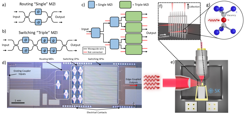
The schematic of our APIC-to-diamond control architecture is as follows. The APIC design consists of a “single” routing Mach-Zender Interferometer (MZI) (Fig. 1a) and a “triple” switching MZI (Fig. 1b) arranged in a binary tree architecture (Fig. 1c). A single cantilever phase shifter (CPS) [22] in the routing MZIs directs the desired amount of light to the appropriate outputs. The switching MZI uses three phase shifters: two CPSs that enable optically broadband and high-fidelity routing ( dB) for cross and bar ports using hardware error correction robust to fabrication imperfections [39] and a third, strain-optic phase shifter (SPS) [41, 21], that enables a fast phase response for on-off switching of the output channel. During operation, a CPU controller programs the two CPSs to route the light to a dump port while the SPS is held at 0 V. We then can send an arbitrary pulse sequence to the SPS to switch the light to the output port without having to change the applied DC voltages to the CPSs.
A microscope image of the APIC is shown in Fig. 1d, with the different phase shifters and electrical contacts labeled. We input light into the chip with an optical fiber array through a single grating leading to the routing MZIs, while other inputs are only used for device calibration. We then collect the edge-coupled light from each output with a high-NA objective, enabling imaging of the outputs into any system for optical control experiments. Figure 1e shows the optical imaging schematic where the output channels are projected into a cryostat to use for optical control of quantum emitters in diamond waveguides (Fig. 1f), such as SiVs (Fig. 1g). This configuration enables perpendicular excitation of the diamond waveguides, with the single photon fluorescence from the emitters coupling to the diamond waveguide mode and emitting vertically for collection through inverse tapered couplers, as shown in Figure 1f. This free-space collection allows for efficient and scalable detection due to low-loss collection optics that are robust to misalignment when compared with fiber coupling or PIC integration. Electrical control of the integrated optical components is made through a custom printed circuit board (PCB) with wire bonds to the APIC. Commercial arbitrary waveform generator boards, embedded in a National Instruments PXIe system, control the CPSs and SPSs. A single board with 22 active channels controls the CPSs, providing 25 V, and two boards with four channels of arbitrary waveform generation each control the SPSs, providing 2.5 V. High-speed amplifiers on the PCB amplify the signals to the SPSs to 12.5 V. See Supplementary Sections 1 and 2 for more details on the optical and electrical components of the system.
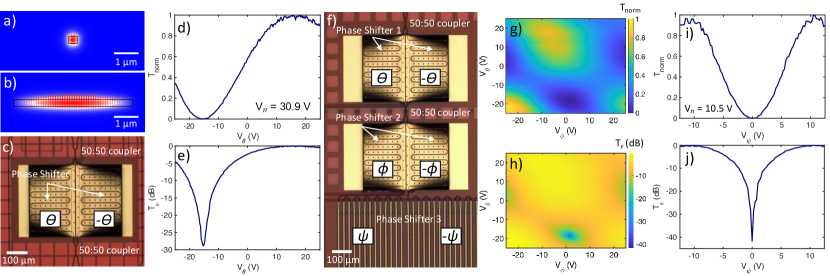
Figure 2 summarizes the APIC characterization and calibration by monitoring the transmission of each edge-coupled optical output. For all optical tests, we use 737 nm wavelength laser light coupled into the TM mode of the on-chip 400 nm wide by 300 nm thick silicon nitride waveguides (modal shape simulated in Fig. 2a), which adiabatically expand to 5 m wide in the SPS (Fig. 2b) to increase strain-optic sensitivity [41, 21]. The less-confined TM mode takes advantage of a higher photoelastic responsivity when compared to the TE mode [42], resulting in a lower of the phase shifter than previously reported [21]. Our DC calibration results for the routing MZIs (Fig. 2c) are shown in Fig. 2d-e and for the switching MZIs (Fig. 2f) are shown in Fig. 2g-j, highlighting the low-voltage operation of the SPS for switching and high on-off extinction ratios. These high extinction ratios for the triple-phase shifter are enabled by the second CPS accounting for fabrication imperfections in the 50:50 directional couplers. For calibration data for each of the output ports, see Supplementary Section 3.
III Pulse Characterization and Stability
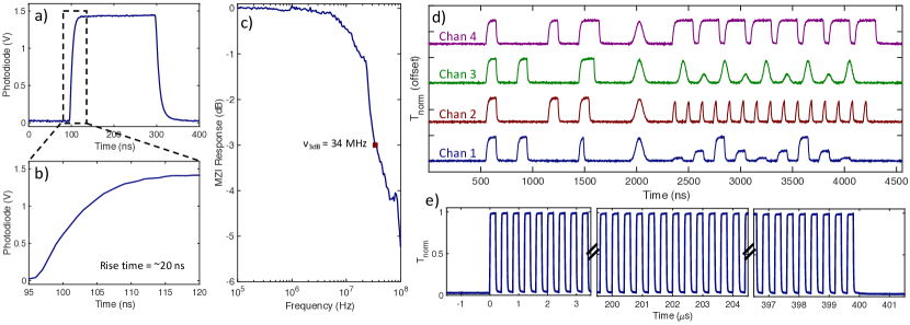
We tested the optical pulse carving of our switch by applying representative pulse sequences to each of the SPSs in the switching MZIs. The “off” state of the output is defined to be 0 V due to the calibration procedure, and the full “on” state is achieved by applying the experimentally determined cross-state voltage. Pulses of varying amplitudes below the maximum are created by setting the applied voltage between these cross and bar states. Using time-resolved measurements on a 125 MHz photodiode, we found rise and fall times of 20 ns when programming a 200 ns pulse (Fig. 3a,b) for all channels. The small-signal frequency-resolved modular response (Fig. 3c) indicates a -3 dB cutoff at = 34 MHz, allowing for MHz optical control of each channel. The device can also be run at higher modulation speeds ( MHz) with a trade-off of lower responsivity ( dB).
To explore the optical control programmability, we tested various pulse sequences. Figure 3d shows the resulting measurement of each of the outputs and shows four different capabilities of this system: i) Any set of outputs can be pulsed simultaneously, ii) each pulse width can be independently manipulated, iii) the waveform can be temporally amplitude modulated into different shapes, such as square or Gaussian, and iv) the pulse height can be independently set. With these criteria met, our chip has the ability to create a full set of quantum rotations [43]. Furthermore, we measured the consistency of the pulsing of our device by applying repeated 200 ns pulses with 200 ns intervals and measuring the deviations in each pulse. We find a pulse area consistency (1 standard deviation) of for 1000 pulses, showing robust pulse uniformity. Examples of these pulses from the beginning, middle, and end of this pulse sequence are shown in Fig. 3e. Lastly, we did not observe crosstalk from either thermal, electrical, or piezo effects between the different phase shifters (details in Supplementary Section 4).
IV Independent addressing of multiple single SiVs
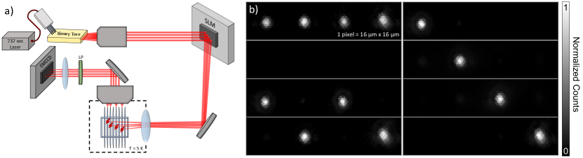
To demonstrate the applicability of the APIC, we used it to resonantly drive individual emitters within an ensemble of SiVs. As shown in Fig. 4a, the APIC projects each port perpendicularly onto separate diamond waveguides in a cryostat. The diamond waveguides are fabricated with inverse tapered end couplers oriented towards the collection path, allowing for a high collection efficiency of 15 (see Methods for full diamond fabrication information and Suplementary Section 5 for collection efficiency calculation). The inverse tapers confine the emitted PL to an NA much smaller than that of the collection optics, allowing for scalable collection. In the excitation path, we include a spatial light modulator (SLM) for small spatial adjustments to each projected beam. This allows us to independently steer each excitation spot to specific SiVs in the diamond waveguides. We note that once the SLM is initially programmed, it is kept static over the course of the experiment, making its slow reconfiguration time (100 Hz) inconsequential for the excitation experiments. We resonantly excite each of the SiVs while collecting the phonon sideband (PSB) emission using a 750 nm long pass filter to remove excess pump light. We projected this fluorescence onto an electron-multiplying charge-coupled device (EMCCD). Figure 4b shows acquisitions of 30 seconds of the collected fluorescence normalized to the brightest point of each image, with no further image processing. This sequence shows independent and simultaneous optical control of SiVs in four different diamond waveguides. Due to variations in the local strain throughout the diamond, the zero-phonon lines (ZPLs) have an inhomogeneous distribution that exceeds the excitation laser linewidth. To collect SiV emission from multiple waveguides simultaneously, we increased the temperature of the diamond samples to broaden the ZPL linewidths so that they are spectrally overlapping. Thus, for these images, we likely addressed multiple emitters in each diamond waveguide due to the high density of SiVs in our sample ( emitters per waveguide).
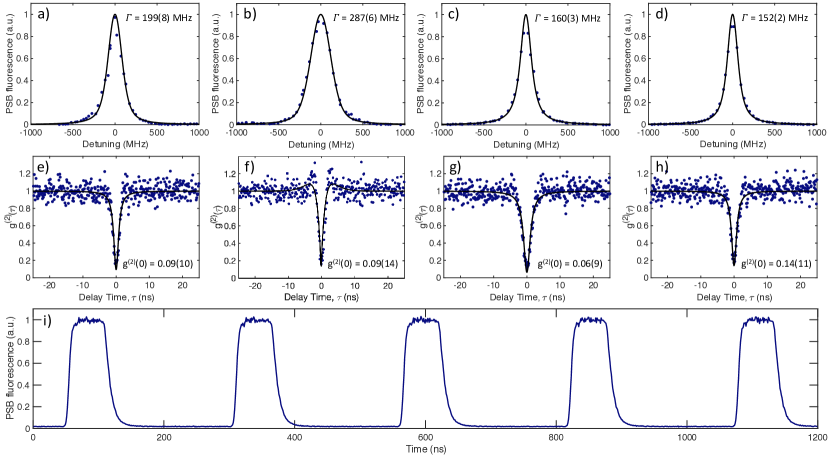
However, to show the applicability of this scheme for controlling individual single emitters, we cooled the diamond sample to a base temperature of 5 K and repeated the excitation scheme with each channel projected onto a spectrally resolved SiV. Figure 5a-d shows the PLE frequency scans for SiVs in four different waveguides, demonstrating linewidths MHz. Second-order correlation measurements indicate strong antibunching, with a normalized (0) ranging from 0.06 0.09 to 0.14 0.11, well below the 0.5 threshold for single photon emission (Fig. 5e-h). We find an average emitter lifetime of 1.76(1) ns (see Supplementary Section 5), consistent with other measurements on ion-implanted SiVs [44]. With the outputs of the MZI tree projected on these emitters simultaneously, we send pulse sequences to temporally control the SiV emission. An example pulse train is shown in Fig. 5i, where we repeatedly pulse one of the channels (Channel 3, Fig. 5c,g) with 100 ns pulses and a period of 250 ns and collect the fluorescence on a time-resolved avalanche photodiode, demonstrating temporal control of a single photon source.
V Discussion
We introduced and demonstrated a scalable optical control system for individual addressing of quantum atom-like emitters. The modularity of the APICs and diamond microchiplets is scalable to 1000s of ports and can be integrated with CMOS control electronics for VSLI devices. Operating voltages can be further reduced by allowing for a trade off of extinction and applied voltage, i.e. if only 30 dB extinction is required then the SPS can be pulsed with V applied signal. The diamond collection architecture is also readily scalable, with high efficiency collection of many waveguides enabled by the modal conversion of the waveguides to a 0.26 NA (See Supplementary Section 6). With the collection optics used in this setup, this allows for the scaling to 2975 waveguides with 3 m spacing between waveguides in a linear array without a loss of collection efficiency. The losses on the chip currently limit the scalability of the platform, with a total measured insertion loss of -19.2 dB. This loss is dominated by a low grating coupler efficiency of , which can be improved with design and fabrication iterations (See Supplementary Section 7 for improved grating coupler results ).
Future work will use this platform for running independent optical control schemes of quantum emitters. Using already demonstrated strain tuning [45, 46], we envision a second chip built from the same APIC platform that allows for spectral matching of quantum emitters, a necessary functionality for quantum computation. More broadly, the broadband [21, 22] APIC technology can be applied to other optically trapped atomic systems [47, 48, 49, 50, 51, 52, 53] and will enable near-future experiments in the area of optical quantum control.
VI Methods
VI.1 PIC Calibration
To begin a calibration, the light from the first output channel is focused onto a photodiode. An iris is used to ensure that only the light from the active output is being measured. A single laptop controls all of the equipment in the experiment and is able to set the applied voltages and query the measured values from the powermeter. We first calibrate the routing MZIs. The applied voltage is swept from -25 V to 25 V in increments of 0.1 V with a power reading at each interval. The voltage is applied differentially to the CPS, with +V being applied to one cantilever and -V applied to the other, nominally giving a and phase shift for each path respectively. During the calibration, all other phase shifters’ voltages are held constant. To find the cross and bar states, we fit an offset sine curve to the data and take the maximum and minimum values.
Next, we calibrate the triple-phase shifter switching MZIs. We begin by setting the voltage of the SPS to 0 V, and then calibrate the CPSs. Since the total extinction of this MZI is dependent on the relationship between and , we do a nested two dimensional sweep of the applied voltages from -25 V to 25 V in increments of 0.25 V. The cross and bar states are found by fitting a two dimensional sinusoid to the data and taking the maximum and minimum values respectively. We then set the two CPSs to their bar state (minimum transmission) and calibrate the SPS by sweeping the voltage from -25 V to 25 V in increments of 0.1 V. The SPSs are also operated differentially in a push-pull configuration. We fit an offset sine curve to this data to find its cross and bar states. With how we set up this calibration, the bar state is defined to be 0 V due to the CPSs being set to their bar state. Full calibration results are shown in the Supporting Information Section 3.
VI.2 Diamond Chiplet Fabrication
For the generation of negatively charged SiV in the diamond, we relieved the strained surface of the diamond plate by removing the top 7 m using Ar/Cl2 plasma etching followed by O2 etching. The sample was subsequently implanted with Si29 at 190 keV with a dose of ions/cm2 (Innovion Inc.). It was then annealed in an ultra-high vacuum furnace ( mbar) at 1200 C and cleaned in a boiling tri-acid mixture (1:1:1 nitric acid, sulfuric acid, and perchloric acid at 345 C). A 180 nm silicon nitride (Si3N4) was chemical vapor deposited on the diamond, and patterned using electron-beam lithography and CF4 reactive-ion etching (RIE). We isotropically undercut the diamond quantum microchiplet (QMC) using an oxygen inductively coupled plasma (ICP) RIE. Lastly, we submerged the sample in hydrofluoric acid to remove the Si3N4 hard mask and alumina [54].
VI.3 SiV Linewidth and Autocorrelation Measurements
The diamond sample used in these experiments was fabricated into a QMC [9] as described above. We then broke the QMC into individual waveguides and placed them overhanging the edge of a cleaved Si chip using tungsten tips. We mounted the Si chip vertically in the Montana cryostat to enable perpendicular excitation and collection.
When measuring the individual SiV emitters, we coupled a single waveguide mode at a time to a multimode fiber for high-efficiency collection. We fit the emitter’s PLE linewidth scans with a Voigt profile using the Nelder-Mead simplex algorithm for the fit optimization. For the autocorrelation measurements, we used a 50:50 fiber splitter to send the light to two APDs in a Hanbury-Brown-Twiss setup. During these measurements, we input pulsed 532 nm light into the waveguide through the collection objective. We input the minimum amount of repump needed to obtain the maximum count rate, providing maximum charge state initialization. We gated the detectors to only collect data when the repump beam is off.
To fit the values, we used a Lorentzian fit to the data.
| (1) |
where is the delay time between coincident counts, and are the offset and scaling factors respectively, is the full-width half-max of the emitter spectrum. For the one emitter that showed pronounced bunching behavior, we fit the data to a three level system and added in an overall offset and scaling factor to account for the non-ideality of the data due to dark counts and jitter from the APD.
| (2) |
where is the delay time between coincident counts, and are the offset and scaling factors respectively, a is the scaling factor determining the strength of the photon bunching, is the antibunching time constant, and is the bunching time constant. When compared to the standard Lorentzian fit, we obtained similar values for (0) (0.09 vs 0.07). The error bars reported in the manuscript correspond to one standard deviation in the fit parameters.
Acknowledgements.
Major funding for this work is provided by MITRE for the Quantum Moonshot Program. D.E. acknowledges partial support from Brookhaven National Laboratory, which is supported by the U.S. Department of Energy, Office of Basic Energy Sciences, under Contract No. DE-SC0012704 and the NSF RAISE TAQS program. M.E. performed this work, in part, with funding from the Center for Integrated Nanotechnologies, an Office of Science User Facility operated for the U.S. Department of Energy Office of Science. M.D. and M.Z. thank MITRE engineers L. Chan, K. Dauphinais, and S. Vergados for their support in building mechanical and electronic components. K.P. and M.D. thank S. Trajtenberg and Y. S. Duan for additional experimental support and C. Li and Y. Hu for helpful conversations and comments.Author Contributions
K.J.P. built the experimental setup and performed the device characterization and calibration experiments. K.J.P. and D.A.G., with assistance from G.C. and M.D., built and performed the SiV direct excitation experiments. K.J.P. performed the data analysis. M.Z. designed the electronic control system. M.D., with assistance from A.M., designed the APIC. M.E. and A.J.L., with assistance from D.D., supervised the APIC fabrication. K.C.C. and L.L. fabricated the diamond microchiplets. K.C.C. performed the diamond waveguide simulations. M.D. and D.E. conceived the experiment and device architecture. M.D., G.G., M.E., and D.E. supervised the project. K.J.P. and M.D. wrote the manuscript with input from all authors.
Additional Information
Supplementary information is available for experimental methods related to programming and calibrating the photonic integrated circuit and collection apparatus.
Competing Interests
D.E. is a scientific advisor to and holds shares in QuEra Computing.
Data Availability
The data that support the plots within this paper are available from the corresponding authors upon reasonable request.
References
- Atatüre et al. [2018] M. Atatüre, D. Englund, N. Vamivakas, S.-Y. Lee, and J. Wrachtrup, Material platforms for spin-based photonic quantum technologies, Nature Reviews Materials 3, 38 (2018).
- Bar-Gill et al. [2013] N. Bar-Gill, L. M. Pham, A. Jarmola, D. Budker, and R. L. Walsworth, Solid-state electronic spin coherence time approaching one second, Nat. Commun. 4, 1743 (2013).
- Bradley et al. [2019] C. E. Bradley, J. Randall, M. H. Abobeih, R. C. Berrevoets, M. J. Degen, M. A. Bakker, M. Markham, D. J. Twitchen, and T. H. Taminiau, A Ten-Qubit Solid-State spin register with quantum memory up to one minute, Phys. Rev. X 9, 031045 (2019).
- Dutt et al. [2007] M. V. G. Dutt, M. V. Gurudev Dutt, L. Childress, L. Jiang, E. Togan, J. Maze, F. Jelezko, A. S. Zibrov, P. R. Hemmer, and M. D. Lukin, Quantum register based on individual electronic and nuclear spin qubits in diamond (2007).
- Stas et al. [2022] P.-J. Stas, Y. Q. Huan, B. Machielse, E. N. Knall, A. Suleymanzade, B. Pingault, M. Sutula, S. W. Ding, C. M. Knaut, D. R. Assumpcao, Y.-C. Wei, M. K. Bhaskar, R. Riedinger, D. D. Sukachev, H. Park, M. Lončar, D. S. Levonian, and M. D. Lukin, Robust multi-qubit quantum network node with integrated error detection, Science 378, 557 (2022).
- Humphreys et al. [2018] P. C. Humphreys, N. Kalb, J. P. J. Morits, R. N. Schouten, R. F. L. Vermeulen, D. J. Twitchen, M. Markham, and R. Hanson, Deterministic delivery of remote entanglement on a quantum network, Nature 558, 268 (2018).
- Hensen et al. [2015] B. Hensen, H. Bernien, A. E. Dréau, A. Reiserer, N. Kalb, M. S. Blok, J. Ruitenberg, R. F. L. Vermeulen, R. N. Schouten, C. Abellán, W. Amaya, V. Pruneri, M. W. Mitchell, M. Markham, D. J. Twitchen, D. Elkouss, S. Wehner, T. H. Taminiau, and R. Hanson, Loophole-free bell inequality violation using electron spins separated by 1.3 kilometres, Nature 526, 682 (2015).
- Sipahigil et al. [2016] A. Sipahigil, R. E. Evans, D. D. Sukachev, M. J. Burek, J. Borregaard, M. K. Bhaskar, C. T. Nguyen, J. L. Pacheco, H. A. Atikian, C. Meuwly, R. M. Camacho, F. Jelezko, E. Bielejec, H. Park, M. Lončar, and M. D. Lukin, An integrated diamond nanophotonics platform for quantum-optical networks, Science 354, 847 (2016).
- Wan et al. [2020] N. H. Wan, T.-J. Lu, K. C. Chen, M. P. Walsh, M. E. Trusheim, L. De Santis, E. A. Bersin, I. B. Harris, S. L. Mouradian, I. R. Christen, E. S. Bielejec, and D. Englund, Large-scale integration of artificial atoms in hybrid photonic circuits, Nature 583, 226 (2020).
- Nielsen and Chuang [2010] M. A. Nielsen and I. L. Chuang, Quantum Computation and Quantum Information: 10th Anniversary Edition (Cambridge University Press, 2010).
- Wehner et al. [2018] S. Wehner, D. Elkouss, and R. Hanson, Quantum internet: A vision for the road ahead, Science 362 (2018).
- Kimble [2008] H. J. Kimble, The quantum internet, Nature 453, 1023 (2008).
- Bogaerts et al. [2020] W. Bogaerts, D. Pérez, J. Capmany, D. A. B. Miller, J. Poon, D. Englund, F. Morichetti, and A. Melloni, Programmable photonic circuits, Nature 586, 207 (2020).
- Christen et al. [2022] I. Christen, M. Sutula, T. Propson, H. Sattari, G. Choong, C. Panuski, A. Melville, J. Mallek, S. Hamilton, P. Benjamin Dixon, A. J. Menssen, D. Braje, A. H. Ghadimi, and D. Englund, An integrated photonic engine for programmable atomic control, arXiv (2022), arXiv:2208.06732 [quant-ph] .
- Desiatov et al. [2019] B. Desiatov, A. Shams-Ansari, M. Zhang, C. Wang, and M. Lončar, Ultra-low-loss integrated visible photonics using thin-film lithium niobate, Optica, OPTICA 6, 380 (2019).
- Li et al. [2022] C. Li, B. Chen, Z. Ruan, H. Wu, Y. Zhou, J. Liu, P. Chen, K. Chen, C. Guo, and L. Liu, High modulation efficiency and large bandwidth thin-film lithium niobate modulator for visible light, Opt. Express 30, 36394 (2022).
- Liang et al. [2021] G. Liang, H. Huang, A. Mohanty, M. C. Shin, X. Ji, M. J. Carter, S. Shrestha, M. Lipson, and N. Yu, Robust, efficient, micrometre-scale phase modulators at visible wavelengths, Nat. Photonics 15, 908 (2021).
- Mohanty et al. [2020] A. Mohanty, Q. Li, M. A. Tadayon, S. P. Roberts, G. R. Bhatt, E. Shim, X. Ji, J. Cardenas, S. A. Miller, A. Kepecs, and M. Lipson, Reconfigurable nanophotonic silicon probes for sub-millisecond deep-brain optical stimulation, Nat Biomed Eng 4, 223 (2020).
- Yong et al. [2022] Z. Yong, H. Chen, X. Luo, A. Govdeli, H. Chua, S. S. Azadeh, A. Stalmashonak, G.-Q. Lo, J. K. S. Poon, and W. D. Sacher, Power-efficient silicon nitride thermo-optic phase shifters for visible light, Opt. Express 30, 7225 (2022).
- Menssen et al. [2022] A. J. Menssen, A. Hermans, I. Christen, T. Propson, C. Li, A. J. Leenheer, M. Zimmermann, M. Dong, H. Larocque, H. Raniwala, G. Gilbert, M. Eichenfield, and D. R. Englund, Scalable photonic integrated circuits for programmable control of atomic systems, arXiv (2022), arXiv:2210.03100 [physics.optics] .
- Dong et al. [2021] M. Dong, G. Clark, A. J. Leenheer, M. Zimmermann, D. Dominguez, A. J. Menssen, D. Heim, G. Gilbert, D. Englund, and M. Eichenfield, High-speed programmable photonic circuits in a cryogenically compatible, visible–near-infrared 200 mm CMOS architecture, Nat. Photonics 16, 59 (2021).
- Dong et al. [2022] M. Dong, D. Heim, A. Witte, G. Clark, A. J. Leenheer, D. Dominguez, M. Zimmermann, Y. H. Wen, G. Gilbert, D. Englund, and M. Eichenfield, Piezo-optomechanical cantilever modulators for VLSI visible photonics, APL Photonics 7, 051304 (2022).
- Wang et al. [2022] J. Wang, K. Liu, M. W. Harrington, R. Q. Rudy, and D. J. Blumenthal, Silicon nitride stress-optic microresonator modulator for optical control applications, Opt. Express 30, 31816 (2022).
- Becker et al. [2018] J. N. Becker, B. Pingault, D. Groß, M. Gündoğan, N. Kukharchyk, M. Markham, A. Edmonds, M. Atatüre, P. Bushev, and C. Becher, All-Optical control of the Silicon-Vacancy spin in diamond at millikelvin temperatures, Phys. Rev. Lett. 120, 053603 (2018).
- Becker et al. [2016] J. N. Becker, J. Görlitz, C. Arend, M. Markham, and C. Becher, Ultrafast all-optical coherent control of single silicon vacancy colour centres in diamond, Nat. Commun. 7, 13512 (2016).
- Neu et al. [2012] E. Neu, M. Agio, and C. Becher, Photophysics of single silicon vacancy centers in diamond: implications for single photon emission, Opt. Express 20, 19956 (2012).
- Robledo et al. [2011] L. Robledo, L. Childress, H. Bernien, B. Hensen, P. F. A. Alkemade, and R. Hanson, High-fidelity projective read-out of a solid-state spin quantum register (2011).
- Hepp et al. [2014] C. Hepp, T. Müller, V. Waselowski, J. N. Becker, B. Pingault, H. Sternschulte, D. Steinmüller-Nethl, A. Gali, J. R. Maze, M. Atatüre, and C. Becher, Electronic structure of the silicon vacancy color center in diamond, Phys. Rev. Lett. 112, 036405 (2014).
- Schröder et al. [2011] T. Schröder, F. Gädeke, M. J. Banholzer, and O. Benson, Ultrabright and efficient single-photon generation based on nitrogen-vacancy centres in nanodiamonds on a solid immersion lens, New J. Phys. 13, 055017 (2011).
- Riedrich-Möller et al. [2014] J. Riedrich-Möller, C. Arend, C. Pauly, F. Mücklich, M. Fischer, S. Gsell, M. Schreck, and C. Becher, Deterministic coupling of a single silicon-vacancy color center to a photonic crystal cavity in diamond, Nano Lett. 14, 5281 (2014).
- Benedikter et al. [2017] J. Benedikter, H. Kaupp, T. Hümmer, Y. Liang, A. Bommer, C. Becher, A. Krueger, J. M. Smith, T. W. Hänsch, and D. Hunger, Cavity-Enhanced Single-Photon source based on the Silicon-Vacancy center in diamond, Phys. Rev. Applied 7, 024031 (2017).
- Lee et al. [2012] J. C. Lee, I. Aharonovich, A. P. Magyar, F. Rol, and E. L. Hu, Coupling of silicon-vacancy centers to a single crystal diamond cavity, Opt. Express 20, 8891 (2012).
- Zhang et al. [2018] J. L. Zhang, S. Sun, M. J. Burek, C. Dory, Y.-K. Tzeng, K. A. Fischer, Y. Kelaita, K. G. Lagoudakis, M. Radulaski, Z.-X. Shen, N. A. Melosh, S. Chu, M. Lončar, and J. Vučković, Strongly Cavity-Enhanced spontaneous emission from Silicon-Vacancy centers in diamond, Nano Lett. 18, 1360 (2018).
- Arjona Martínez et al. [2022] J. Arjona Martínez, R. A. Parker, K. C. Chen, C. M. Purser, L. Li, C. P. Michaels, A. M. Stramma, R. Debroux, I. B. Harris, M. Hayhurst Appel, E. C. Nichols, M. E. Trusheim, D. A. Gangloff, D. Englund, and M. Atatüre, Photonic indistinguishability of the Tin-Vacancy center in nanostructured diamond, Phys. Rev. Lett. 129, 173603 (2022).
- Bhaskar et al. [2017] M. K. Bhaskar, D. D. Sukachev, A. Sipahigil, R. E. Evans, M. J. Burek, C. T. Nguyen, L. J. Rogers, P. Siyushev, M. H. Metsch, H. Park, F. Jelezko, M. Lončar, and M. D. Lukin, Quantum nonlinear optics with a Germanium-Vacancy color center in a nanoscale diamond waveguide, Phys. Rev. Lett. 118, 223603 (2017).
- Andrew Golter et al. [2022] D. Andrew Golter, G. Clark, T. El Dandachi, S. Krastanov, A. J. Leenheer, N. H. Wan, H. Raniwala, M. Zimmermann, M. Dong, K. C. Chen, L. Li, M. Eichenfield, G. Gilbert, and D. Englund, Multiplexed control of spin quantum memories in a photonic circuit, arXiv (2022), arXiv:2209.11853 [quant-ph] .
- Mouradian et al. [2015] S. L. Mouradian, T. Schröder, C. B. Poitras, L. Li, J. Goldstein, E. H. Chen, M. Walsh, J. Cardenas, M. L. Markham, D. J. Twitchen, M. Lipson, and D. Englund, Scalable integration of Long-Lived quantum memories into a photonic circuit, Phys. Rev. X 5, 031009 (2015).
- Miller [2015] D. A. B. Miller, Perfect optics with imperfect components, Optica 2, 747 (2015).
- Wang et al. [2020] M. Wang, A. Ribero, Y. Xing, and W. Bogaerts, Tolerant, broadband tunable 2 2 coupler circuit, Opt. Express 28, 5555 (2020).
- Sukachev et al. [2017] D. D. Sukachev, A. Sipahigil, C. T. Nguyen, M. K. Bhaskar, R. E. Evans, F. Jelezko, and M. D. Lukin, Silicon-Vacancy spin qubit in diamond: A quantum memory exceeding 10 ms with Single-Shot state readout, Phys. Rev. Lett. 119, 223602 (2017).
- Stanfield et al. [2019] P. R. Stanfield, A. J. Leenheer, C. P. Michael, R. Sims, and M. Eichenfield, CMOS-compatible, piezo-optomechanically tunable photonics for visible wavelengths and cryogenic temperatures, Opt. Express 27, 28588 (2019).
- Gyger et al. [2020] F. Gyger, J. Liu, F. Yang, J. He, A. S. Raja, R. N. Wang, S. A. Bhave, T. J. Kippenberg, and L. Thévenaz, Observation of stimulated brillouin scattering in silicon nitride integrated waveguides, Phys. Rev. Lett. 124, 013902 (2020).
- Li et al. [2011] J.-S. Li, J. Ruths, T.-Y. Yu, H. Arthanari, and G. Wagner, Optimal pulse design in quantum control: a unified computational method, Proc. Natl. Acad. Sci. U. S. A. 108, 1879 (2011).
- Wang et al. [2005] C. Wang, C. Kurtsiefer, H. Weinfurter, and B. Burchard, Single photon emission from SiV centres in diamond produced by ion implantation, J. Phys. B At. Mol. Opt. Phys. 39, 37 (2005).
- Meesala et al. [2018] S. Meesala, Y.-I. Sohn, B. Pingault, L. Shao, H. A. Atikian, J. Holzgrafe, M. Gündoğan, C. Stavrakas, A. Sipahigil, C. Chia, R. Evans, M. J. Burek, M. Zhang, L. Wu, J. L. Pacheco, J. Abraham, E. Bielejec, M. D. Lukin, M. Atatüre, and M. Lončar, Strain engineering of the silicon-vacancy center in diamond, Phys. Rev. B Condens. Matter 97, 205444 (2018).
- Clark et al. [2022] G. Clark, M. Koppa, K. Chen, A. Leenheer, L. Li, D. Dominguez, M. Dong, M. Saha, D. A. Golter, G. Gilbert, M. Eichenfield, and D. Englund, Piezoelectric control of spin quantum memories in a cryogenic programmable photonic circuit platform, in 2022 Conference on Lasers and Electro-Optics (CLEO) (2022) pp. 1–2.
- Debnath et al. [2016] S. Debnath, N. M. Linke, C. Figgatt, K. A. Landsman, K. Wright, and C. Monroe, Demonstration of a small programmable quantum computer with atomic qubits, Nature 536, 63 (2016).
- Niffenegger et al. [2020] R. J. Niffenegger, J. Stuart, C. Sorace-Agaskar, D. Kharas, S. Bramhavar, C. D. Bruzewicz, W. Loh, R. T. Maxson, R. McConnell, D. Reens, G. N. West, J. M. Sage, and J. Chiaverini, Integrated multi-wavelength control of an ion qubit, Nature 586, 538 (2020).
- Ebadi et al. [2021] S. Ebadi, T. T. Wang, H. Levine, A. Keesling, G. Semeghini, A. Omran, D. Bluvstein, R. Samajdar, H. Pichler, W. W. Ho, S. Choi, S. Sachdev, M. Greiner, V. Vuletić, and M. D. Lukin, Quantum phases of matter on a 256-atom programmable quantum simulator, Nature 595, 227 (2021).
- Pino et al. [2021] J. M. Pino, J. M. Dreiling, C. Figgatt, J. P. Gaebler, S. A. Moses, M. S. Allman, C. H. Baldwin, M. Foss-Feig, D. Hayes, K. Mayer, C. Ryan-Anderson, and B. Neyenhuis, Demonstration of the trapped-ion quantum CCD computer architecture, Nature 592, 209 (2021).
- Lambrecht et al. [2017] A. Lambrecht, J. Schmidt, P. Weckesser, M. Debatin, L. Karpa, and T. Schaetz, Long lifetimes and effective isolation of ions in optical and electrostatic traps, Nat. Photonics 11, 704 (2017).
- Levine et al. [2019] H. Levine, A. Keesling, G. Semeghini, A. Omran, T. T. Wang, S. Ebadi, H. Bernien, M. Greiner, V. Vuletić, H. Pichler, and M. D. Lukin, Parallel implementation of High-Fidelity multiqubit gates with neutral atoms, Phys. Rev. Lett. 123, 170503 (2019).
- Graham et al. [2022] T. M. Graham, Y. Song, J. Scott, C. Poole, L. Phuttitarn, K. Jooya, P. Eichler, X. Jiang, A. Marra, B. Grinkemeyer, M. Kwon, M. Ebert, J. Cherek, M. T. Lichtman, M. Gillette, J. Gilbert, D. Bowman, T. Ballance, C. Campbell, E. D. Dahl, O. Crawford, N. S. Blunt, B. Rogers, T. Noel, and M. Saffman, Multi-qubit entanglement and algorithms on a neutral-atom quantum computer, Nature 604, 457 (2022).
- Mouradian et al. [2017] S. Mouradian, N. H. Wan, T. Schröder, and D. Englund, Rectangular photonic crystal nanobeam cavities in bulk diamond, Appl. Phys. Lett. 111, 021103 (2017).