Efficient Intra-Rack Resource Disaggregation for HPC Using Co-Packaged DWDM Photonics
Abstract
The diversity of workload requirements and increasing hardware heterogeneity in emerging high performance computing (HPC) systems motivate resource disaggregation. Resource disaggregation allows compute and memory resources to be allocated individually as required to each workload. However, it is unclear how to efficiently realize this capability and cost-effectively meet the stringent bandwidth and latency requirements of HPC applications. To that end, we describe how modern photonics can be co-designed with modern HPC racks to implement flexible intra-rack resource disaggregation and fully meet the bit error rate (BER) and high escape bandwidth of all chip types in modern HPC racks. Our photonic-based disaggregated rack provides an average application speedup of 11% (46% maximum) for 25 CPU and 61% for 24 GPU benchmarks compared to a similar system that instead uses modern electronic switches for disaggregation. Using observed resource usage from a production system, we estimate that an iso-performance intra-rack disaggregated HPC system using photonics would require 4 fewer memory modules and 2 fewer NICs than a non-disaggregated baseline.
I Introduction
Leading HPC systems are steadily embracing heterogeneity of compute and memory resources to preserve performance scaling and reduce system power [1, 2, 3]. This trend is already apparent with the integration of GPUs [4, 5, 6] and is expected to continue with fixed-function or reconfigurable accelerators such as field programmable gate arrays [7, 8, 9, 10, 11, 12, 13], and heterogeneous memory [14]. Also, key HPC workloads show considerable diversity in computational and memory access patterns [15, 16].
This expectation of resource heterogeneity, workload diversity, and today’s method of allocating resources to applications in units of statically-configured nodes where every node is identical and unused resources are left to idle (referred to as “marooned resources”), raises the concern of resource underutilization. Marooned resources increase capital and operational costs without improving performance. This has motivated resource disaggregation. Disaggregation refers to decomposing servers into their constituent compute and memory resources so that these can be allocated as required according to the needs of each workload. Hyperscale datacenters have embraced resource disaggregation and showed that it significantly improves utilization of GPUs and memory [17, 18, 19, 20, 21, 22, 23, 24, 25, 26, 27, 28].
Although file storage is routinely disaggregated in modern systems [29, 15, 30], HPC has been slow to embrace disaggregation of compute and memory resources [31, 32] due to the sensitivity of HPC workloads to bandwidth and latency that cannot be met by current PCIe/CXL or Ethernet link technologies used in contemporary disaggregated architectures. Studies showed that disaggregation only among resources in the same rack (i.e., intra-rack resource disaggregation) in HPC could reduce resources by 5.36% to 69.01% while avoiding the overhead of full-system disaggregation [15]. However, the impact of increased memory latency and specific architectural trade-offs have not been explored. Thus, although disaggregation using electronic networks has been demonstrated in hyperscale datacenters [33, 22, 34, 26], minimizing adverse effects to and addressing the stringent bandwidth density and latency demands of HPC workloads requires a thorough investigation.
Our contributions are as follows. Firstly, we describe how to use emerging photonic links and switches to design modern and practical resource-disaggregated HPC racks based on an existing GPU-accelerated HPE/Cray EX supercomputer [29]. Secondly, we show how state-of-the-art commercially available photonic components and advanced packaging multi chip modules meet BER requirements, impose only a 5% power overhead, and deliver sufficient bandwidth to satisfy the escape bandwidth of all chips in modern HPC racks. Thirdly, we show how to use distributed indirect routing and arrayed waveguide grating routers [35, 36] to satisfy all bandwidth requirements without the overhead and latency for reconfiguration that spatial [37, 38] and wave-selective [39] switches require. Furthermore, we show that intra-rack disaggregation using emerging photonics provides an average application speedup of 11% (46% maximum) for 25 CPU and 61% for 24 GPU benchmarks compared to a similar system that instead uses state-of-the-art electronic switches. Finally, based on observed resource usage, we estimate that a system based on state-of-the-art photonics for resource disaggregation can have 4 fewer memory modules and 2 fewer NICs, thus 44% fewer overall chips compared to a non-disaggregated system with the same computational throughput.
II Related Work
Hyperscale datacenters predominantly focus on full-system resource disaggregation where applications can allocate fine-grain resources of different types, today typically graphical processing units [17] and memory [18, 40, 21, 23, 26, 28]. In such a system, resources of the same type are typically placed in the same rack [33, 22, 34].
However, full-system, flexible, and fine-grain resource disaggregation introduces significant overhead because of the higher latency and lower bandwidth density of contemporary hardware used to implement resource disaggregation – typically PCIe, 100Gig Ethernet, and eventually compute express link (CXL) [41] over electronic links. This overhead does not simply increase power and procurement costs. Instead, it adds potentially substantial latency between key resources such as central processing units and memory traditionally exhibit latency-sensitive communication. The aforementioned studies quote several orders of magnitude increase in network and memory latency due to full-system resource disaggregation to improve resource utilization by 35% at most [42]. Another study found that application performance degradation depends on both network bandwidth and latency, but can still reach 40% even with high bandwidth, low-latency networks [43]. Work on SPEC and commercial benchmarks also found an up to 27% application slowdown due to the additional memory latency [44]. A study on Microsoft’s Azure found a range of performance slowdowns up to 30% from an extra 65 ns to access main memory [20]; a later study reported a range of slowdowns with a mean of 10%, a higher average, and a maximum of about 100% from an additional 142 ns. \AcpSDN based on electrical networks fare no better in terms of overhead [43, 45, 34].
Hybrid full-system photonic–electronic approaches have also been proposed that rely on circuit switching [42]. A few studies argue that intra-rack disaggregation [19, 40, 25] or disaggregation among small groups of CPUs [26, 28] suffice to recover most gains. Even the low latency and high bandwidth density of modern photonics can only partially satisfy the bandwidth, energy, and latency requirements of full system disaggregation. This makes system-wide disaggregation impractical in many cases [33, 42, 24, 46].
Recent full system approaches in HPC rely on optics to connect CPUs and memory, and electronic switches for hard disk drives to increase resource CPU utilization by 36.6% and memory 21.5% [32]. Another study argues that HPC systems can reduce resources from 5.36% to 69.01% with intra-rack disaggregation and still satisfy the worst-case average rack utilization [15]. Similar to datacenters, intra-rack disaggregation in HPC promises the lowest overhead and impact to applications [31, 19, 25].
Related work has researched other aspects necessary to make resource disaggregation practical in a system, such as job scheduling [47, 48, 49, 50], how the operating system (OS) and runtime should adapt [51, 52, 53], page migration policies and temporal imbalance [27, 28], programming and code portability in heterogeneous systems [54, 48], partitioning of application data [55], fault tolerance [56], how to fairly compare the performance of different heterogeneous systems [57], and the impact of heterogeneous resources to application performance [58, 59, 14]. These are important but out of scope topics for our study.
II-A Under-utilization in Production Systems
We use NERSC’s Cori as an exemplar production HPC system due to its diverse and open-science workload, while recognizing workload requirements on other systems may differ. In NERSC’s Cori, at a time before Perlmutter became available and thus Cori was serving the full NERSC workload, three quarters of the time, Haswell nodes use less than 17.4% of memory capacity (50.1% for KNL nodes) and less than 0.46 GB/s of memory bandwidth [15]. These observations are similar to observations made on LANL clusters [18] and Alibaba machines that execute batch jobs. Likewise, half of the time, Cori nodes use no more than half of their compute cores and three quarters of the time 1.25% of available network interface controller (NIC) bandwidth. Similarly, in Lawrence Livermore National Laboratory clusters, approximately 75% of the time, no more than 20% of memory capacity is used [18]. Alibaba’s published data [60] show that memory is underutilized similar to Cori, for machines that execute batch jobs. Data from Google systems shows that task memory and disk capacity is spread over three orders of magnitude and typically underutilized [45]. Azure reports approximately 25% of memory under-utilization [20, 26]. Datacenters have also reported 28% to 55% CPU idle in the case of Google trace data [61] and 20%–50% usually in Alibaba [60]. Early studies also suggest GPU under-utilization [62, 63, 64].
III Photonics for Resource Disaggregation
Here we show that photonic links and switches today meet the strict performance and error rate requirements to efficiently implement intra-rack resource disaggregation in HPC.
III-A Memory Technologies and Requirements
IO systems in HPC are already largely disaggregated over conventional system-scale interconnects since the underlying technologies (disk or SSD) are relatively high latency and lower bandwidth [15, 65]. In contrast, memory technologies, particularly high bandwidth memory (HBM) needed by GPUs, are much higher bandwidth and much less tolerant of latency and require much lower BERs. Given that memory disaggregation imposes the most challenging constraints among other resources in today’s compute nodes, we will use DDR and HBM memory technology to set our performance target. A typical DDR4 memory has a response latency of approximately 90 ns, and for HBM, the average response latency is 90-140 ns [66]. Still, any added latency between the CPU and memory from resource disaggregation may penalize application performance, as we quantify later. Server-class memories typically require BERs of less than to achieve tolerable failures in time (FIT) rates with conventional single-error-correct/double-error-detect (SEC-DED) protection [67, 68]. \AcFEC can reduce the BER, but with additional latency [69].
III-B Optical Link Technologies
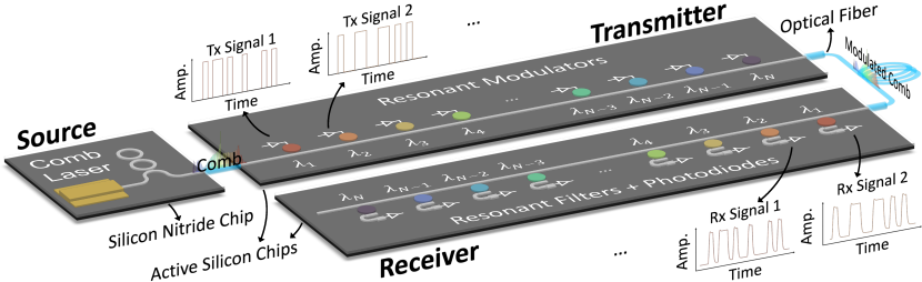
We consider a range of photonic link technologies that include conventional 100 Gbps Ethernet physical interfaces that represent the current baseline link technology for memory disaggregation. We also introduce a range of cutting-edge dense wavelength division multiplexing (DWDM) link technologies that are either demonstrated as research prototypes or are commercially available. All photonic components come from existing commercial technologies (100 Gbps, 400 Gbps, Ayar TeraPhy) and some research prototypes from DARPA PIPES (the 1-2 Tbps link technologies). These higher performance link technologies must be co-packaged to achieve their bandwidth density. These link technologies are summarized in Table I. The technology for the optical links is depicted in Figure 1. Delivering multiple channels of laser light to the package has been challenging to scale cost-effectively if each “color” of light were to require a separate laser source. This concern was alleviated by the emergence of quantum dot and soliton comb laser sources that can produce hundreds of usable light frequencies with wall-plug efficiencies of up to 41% [70].
III-C Active Photonic MCMs
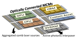
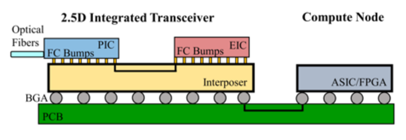
Many CPUs and GPUs do not have the necessary off-chip bandwidth for full utilization of their compute resources because operating their I/O pins at a higher bandwidth incurs a power cost [71, 72]. Using emerging high-speed optical links directly to the MCM, illustrated in Figure 3, provides to the order of gains in escape bandwidth [31, 73, 74, 75]. This is a necessary property to enable efficient resource disaggregation as well as handle changing bandwidth requirements of key applications such as machine learning that drastically shifts bandwidth between inter-GPUs and off-chip from inference to training.
MCMs with integrated photonics have been demonstrated in both 2.5D and 3D interposer platforms [31, 76, 77, 78]. They can use different die-to-die link standards, such as UCIe. Active interposer platforms combine the photonic integrated circuit (PIC) and interposer into a single integrated substrate. The active interposer allows photonic components to be fabricated and directly integrated with through silicon vias and additional metal redistribution layers. Electronic circuits are flip-chipped on top of active interposers using copper pillars [79]. Further work has embedded photonic switch fabrics within MCM platforms with a crosstalk suppression and extinction ratio of 50dB and on-chip loss as low 1.8dB [31]. This was further scaled up to support more than 100 ports with microring resonators using a scalable switch fabric that combined switching in the space domain with wavelength-selectivity to implement fine-grain connectivity for node disaggregation [39, 31].
| BW (Gbps) | Energy (pJ/bit) | Link Gbps Channels | #Links (2 TB/s escape) | Agg. Ws (2 TB/s escape) | Ref. |
| 100 | 30 | 160 | 480 | [80, 81] | |
| 400 | 30 | 40 | 197 | [82] | |
| 768 | 1 | 21 | 14.4 | [73] | |
| 1,024 | 0.45 | 16 | 7.2 | [83] | |
| 2,048 | 0.3 | 8 | 4.8 | [83] |
III-C1 Link Protocol
We adopt CXL as our link protocol [41]. CXL is an overlay on the PCIe-Gen6 physical layer; it includes guaranteed ordering of events and is a broadly adopted industry standard with published specifications. However, we do not rely on any features of any particular protocol. Thus, alternatives such as UCIe also apply.
III-C2 Link Propagation and Encoding/Decoding Latency
The target reach for an intra-rack disaggregation solution is approximately 1-4 meters. Given the speed of light and light propagating through optical material with an index of refraction near r1.5, the effective latency of propagating through an optical fiber at nominally 0.75 is approximately 5 ns per meter. Therefore, rack-scale resource disaggregation adds 5-20 ns of latency, approximately less than 20% of the typical DRAM latency. The link latency for SERDES and photonic ring modulation is negligible. Intra-rack fiber lengths up to 4 meters require no intervening optical electrical optical (OEO) conversions.
III-C3 Bit Error Rates and FEC
To achieve BER required for memory technologies, forward error correction (FEC) [69] will likely be required. Using the lightweight FEC scheme that is proposed for CXL [41] and PCIe Gen6 [84] as an example, the all-inclusive latency for FEC can be as low as 2 ns. Therefore, for 200 Gbps, the serialization delay is 10 ns and the FEC calculations add 2-3 ns. At 400 Gbps and above, the net latency for FEC would be 5 ns plus 2-3 ns. Notably, this approach to achieving these BER targets is achievable with less than a 0.1% bandwidth loss.
In terms of impact on BER, this PCIe/CXL-like correction scheme corrects all single bursts of up to 16 bits. Double bursts will likely be mis-corrected, but the chance of a bad flit decreases quadratically (e.g., a flit BER of becomes as you need two error bursts per flit to fail). Each flit is protected with a strong 64-flit CRC such that the flit FIT rate (CRC escapes) is significantly less than one part per billion. Lastly, FEC escapes become link retransmissions and the ASIC-to-ASIC connection sees close to zero errors. As a result, emerging memory fabric protocols such as CXL, which could be run over our evaluated physical links, are capable of achieving a BER rate that meets the stringent memory system requirements and minimizes performance loss due to retransmission.
III-D Optical Switch Technologies
Motivated by minimizing latency, our vision for a disaggregated rack is to have photonically-enabled MCMs that are connected via an optical circuit switch, as shown in Figure 2. Compute and memory chips would be in the center of the MCM and the edge of the MCM would contain co-packaged optical silicon in-package photonics. Switches with all-optical paths include spatial- and wave-selective approaches, shown in Table II.
| Switch Type | Radix | Wave-lengths per port | B/W per channel (wavelength) | Insertion Loss | Crosstalk |
|---|---|---|---|---|---|
| Mach-Zehnder based [85] | 1 | 439 Gbps | 12.8 dB | -26.6 dB | |
| MEMS-actuated [86] | 1 | – | 9.8 dB | -70 dB | |
| Microring resonator [87, 88] | () | 8 (128) | 100 Gbps (42 Gbps) | 5dB (10dB) | (-35 dB) |
| Casc. AWGRs [89] | 370 | 25 Gbps | 15 dB | -35 dB |
III-D1 Spatial Optical Switches
In recent years, the primary switching cells investigated are microelectromechanical systems (MEMS) actuated couplers, Mach-Zehnder interferometers, and microring resonators. Taking after their free-space counterpart, photonic MEMS-actuated switches are broadband spatial switches that have demonstrated radix scaling up to [86]. Although they typically offer low inter-channel crosstalk and low optical losses, MEMS switching cells generally require high driving voltages (greater than 20 V), making them less attractive for co-integration with electronic drivers. Spatial switches can also use mirrors [90], photonic integrated circuits [38], or tiled planar silicon photonics [37]. MZI switches are more friendly to co-integration compared to MEMS but have only been shown to scale up to [85]. This limit can be seen as a consequence of the higher insertion-loss scaling resulting from cascaded MZI cells and the susceptibility of popular MZI topologies to first-order crosstalk.
The challenge for scaling up the spatial approach is the quantization of package and MCM escape bandwidth and reduced configuration options. For example, at 768 Gbps (the Ayar TeraPhy [73]), the number of fibers escaping the package is 21, meaning the package can be connected only up to 21 different potential destinations using a spatial switch.
III-D2 Wavelength Selective Optical Switches and AWGRs
The inherent wavelength-selectivity of MRR switching cells allows for the straightforward implementation of wavelength-selective switching (WSS) topologies. This enables one to establish all-to-all networks by leveraging wavelength-division multiplexing (WDM). Currently, MRR-based switches with the largest radix include the crossbar [87] and switch-and-select [91], but have been experimentally emulated to include a Clos [92]. The metrics in [92] can be seen to correlate very closely with the scaling proposed in [88], making a practical case for the shown in Table II.
All-to-all networks via WDM signals can also be achieved by AWGRs [35, 36, 93, 94, 65]. As AWGRs are passive optical elements, no reconfiguration is possible within the routing fabric itself. Instead, fast wavelength-tunable lasers must be leveraged at the transmitter of every node if it wishes to address a different destination since AWGRs shuffle the light frequencies such that one lambda goes to each endpoint from each source. AWGRs enable us to implement an all-to-all topology using just fibers (each carrying frequencies of light). In contrast, an implementation using copper would require wires. Although the cost of fast wavelength-tunable lasers is still an ongoing research topic [95], AWGRs are mature, commercially available, and well established in literature [96].
In AWGRs, only a limited number of ports can be practically supported due to the walk-off of passband center frequencies from the carrier wavelength grid and the worse crosstalk associated with a larger number of ports (). A feasible implementation of AWGR-based optical switches with a large has been demonstrated utilizing cascaded small-size AWGRs [89]. Specifically, AWGRs (front-AWGRs) are interconnected with AWGRs (rear-AWGRs) to effectively act as an AWGR. Each output port of a front-AWGR is connected to an input port of a rear-AWGR, where the interconnection pattern can be optimized with knowledge of port-specific insertion losses to minimize the worst-case end-to-end insertion loss. Further up-scaling of the switch radix can be achieved by interconnecting small delivery-coupling switchs with multiple copies of the AWGRs, yielding a switching capability. This architecture has been verified by hardware prototypes of and [97, 98], showing 15 dB insertion loss and below dB crosstalk suppression. In order to accommodate the 350 MCMs of our rack, a reasonable configuration is . This results in 370 ports and 370 wavelengths per port (Table II). Since AWGRs typically have a 25 GHz optical bandwidth if the wavelength grid is 50 GHz, with PAM4, we assume 25 Gbps per wavelength [92, 99].
Wave-selective switches [39, 100] can steer any subset of wavelengths to a given destination, not just all (spatial) or one (AWGR). Dynamic programming methods can avoid sending the same frequency of light from two different sources to the same destination. Since this is a relatively new technology, we constructed a model shown in Table II that projects the performance of a larger radix switch comprised of smaller demonstrated building blocks.
III-D3 Reconfiguration Time
Spatial and wave-selective switches typically require centralized scheduling [101] to reach a steady globally optimal solution. The reconfiguration time can range from tens of nanoseconds to tens of milliseconds. In production HPC systems, multi-node jobs start every few seconds and last from minutes to hours [102, 15]. Also, job resource usage and communication become predictable early, do not change fast, and typically remain predictable throughout a job’s execution time [15, 102, 103, 104]. Therefore, even milliseconds of reconfiguration time is ample.
IV Control Logic
Here we describe how we can perform indirect routing to increase point-to-point bandwidth using only per-source logic.
IV-A Indirect routing in AWGRs
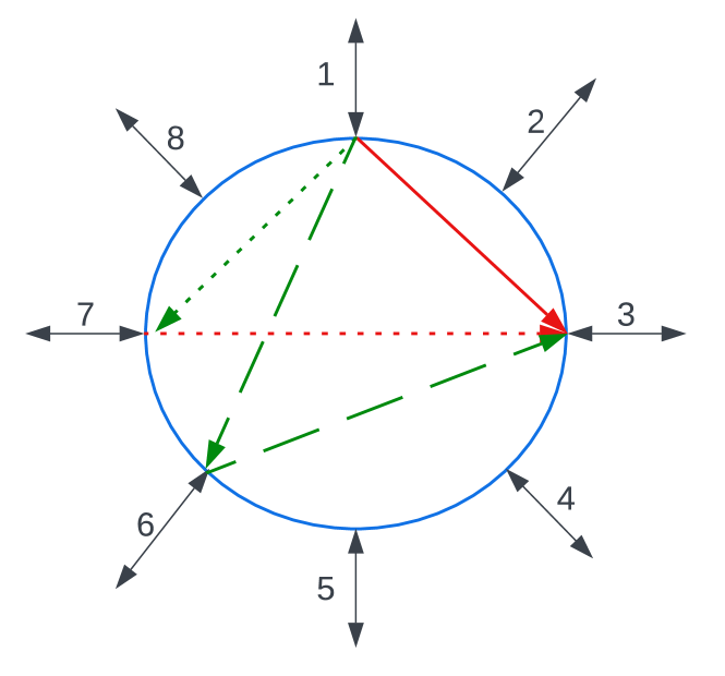
AWGRs dedicate exactly one wavelength between any source–destination pair. If a source–destination pair requires more bandwidth than what a single wavelength can satisfy, sources can use indirect routing, an example of which is shown in Figure 4. Sources can split traffic to intermediate destinations in parallel in order to use the bandwidth of wavelengths. This does not consume additional power in the photonic components assuming lasers are constantly powered. Sources consider indirect paths only if the direct (single-hop) bandwidth to their desired destination does not suffice. A source considers indirect destinations for which the direct bandwidth from the source is available and whose wavelength from the intermediate hop to the desired final destination is also available. Among potentially multiple candidates, sources can choose one in a Valiant fashion [35, 101, 105]. This is done on a per-flow basis in order to avoid out of order packet delivery. This routing can be modeled as a well-established allocation problem and implemented with a low latency and area penalty [106, 107].
Indirect routing relies on sources knowing which other sources attached to the same AWGR are utilizing their local wavelengths in order to identify a productive intermediate destination. For instance, in Figure 4, source 1 should know whether the wavelengths from 7 to 3 and 6 to 3 are occupied. For that, we rely on piggybacking, where traffic between a source–destination pair periodically includes the state of the sources’ wavelengths as a way to broadcast the local state to the rest of the sources attached to the same AWGR [108]. In the case of an AWGR, each source uses bits to encode which of its local wavelengths are occupied with one-hot encoding; Even if we piggyback this information multiple times a second, the bandwidth impact is negligible. For instance, if we multiplex multiple flows into a wavelength and therefore denote 8 bits per wavelength, the status vector per source becomes just . If, due to stale information, sources pick an intermediate destination whose direct wavelength to the final destination is not available, the intermediate destination performs indirect routing through a second intermediate destination. If no messages would otherwise be exchanged between a pair, thus presenting no opportunity for piggybacking, that pair can exchange a separate control message.
IV-B Spatial and Wave-Selective Switches
Spatial and wave-selective switches can use indirect routing in tandem with reconfiguration. Indirect routing reduces the need for reconfiguration, but intermediate destinations should be chosen among destinations that already have a direct connection with the final destination; otherwise, the intermediate destination itself may trigger a reconfiguration. The synergy between indirect routing and switch reconfiguration was explored in [101]. Our proposed design based on AWGRs avoids reconfiguration entirely (Section VI-A1).
V Disaggregated Rack Design
For the rest of our study, we will model an HPC rack based on a GPU-accelerated HPE/Cray EX Supercomputer [29] where a rack contains 128 GPU-accelerated nodes. Each node of our model system contains an AMD Milan CPU with eight memory controllers, each supporting a 3200MHz DDR4 module. Therefore, each CPU has 256 GB of memory with a maximum bandwidth of 204.8 GBps. A compute node also has four NVIDIA Ampere A100 GPUs. Each GPU supports 12 third generation NVLink links, each supporting 25 GBps per direction. Each GPU also has 40 GB of co-located HBM with a bandwidth of 1555.2 GBps. Each node also has four 31.5 GBps PCI Gen4 links to connect each GPU to the CPU. The CPU also connects to four Slingshot 11 NICs with 200 Gbps per direction [109].
V-A MCMs and Escape Bandwidth
We organize chips within each rack into an MCMs package. For simplicity, we restrict all MCMs to have the same escape bandwidth and we place chips of only the same type in MCMs. We then make conservative assumptions for next generation photonics that are entering the market today based on our analysis of Section III. In particular, each MCM has 32 optical fibers attached to it, a conservative assumption compared to the five arrays of 24 fibers demonstrated in [110]. Each fiber supports 64 wavelengths (channels) of 25 Gbps each for a 6400 GBps escape bandwidth per MCM. We vary the number of chips per MCM such that each chip enjoys the same escape bandwidth as in our baseline rack [29]. Therefore, our photonic architecture does not restrict chip escape bandwidth. Table III shows the number of chips per MCM and the total number of MCMs containing chips of that type to satisfy chip escape bandwidth. Each MCM contains a controller chip that interfaces the native protocol of the disaggregated resource to the CXL protocol over the photonic links. CXL’s overhead and its associated FEC is included in our architecture model.
| Chip type | Chips per MCM | MCMs per rack |
|---|---|---|
| CPU | 14 | 10 |
| GPU | 3 | 171 |
| NIC | 203 | 3 |
| HBM | 4 | 128 |
| DDR4 | 27 | 38 |
| Total | 350 |
V-B Optical Switches
The radix and wavelengths per port of optical switches dictate the number of MCMs we can fully connect optically with a single photonic switch as well as the amount of direct (single-hop) bandwidth. From Section III-D, we pick state-of-the-art representatives of wave-selective, cascaded AWGRs, and spatial optical switches. Their parameters are shown in Table IV. Even though spatial [86] and wave-selective switches [39] are capable of 100 Gbps per wavelength, most links available widely today do not support that (Table I). In addition, we show that we can still satisfy bandwidth demands with the conservative assumption of 25 Gbps per wavelength.
| Switch type | State of the art | |
|---|---|---|
| Switch radix | Cascaded AWGRs [89] | 370 |
| Spatial [86] | 240 | |
| Wave-Selective [39] | 256 | |
| Gbps per wavelength | All switches | 25 |
| Wavelengths per port | Cascaded AWGRs [89] | 370 |
| Spatial [86] | 240 | |
| Wave-Selective [39] | 256 |
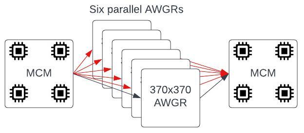
To connect our 350 MCMs using AWGRs, we can combine MCM fibers in five groups of six and connect each group to one port of five parallel AWGRs. However, each AWGR port would be required to handle 384 wavelengths. To respect the per port 370 wavelength limitation of our AWGR configuration but still satisfy the full escape bandwidth of MCMs, we combine the remaining 14 wavelengths along with the remaining two fibers per MCM ( wavelengths total) that were left unconnected into an extra parallel AWGR, for a total of six parallel AWGRs. We then connect MCM fibers to AWGRs in a staggered manner such that each MCM connects to each other MCM using at least five 25 Gbps direct-path wavelengths, for a direct MCM–MCM bandwidth of Gbps. This is illustrated in Figure 5.
For simplicity, because of their relative small difference and because wave-selective switches can also achieve configurations that spatial switches can, we treat both wave-selective and spatial switches as 256 ports with 256 wavelengths per port. Each MCM can connect to parallel switches. However, because the radix of optical switches is lower than the number of MCMs, we instantiate 11 optical switches and connect MCMs in a staggered manner such that an optical switch with an index connects to MCMs that have an index starting from until . This way, a small number of optical switch ports are left unconnected to not exceed the 32 fibers per MCM. These ports can support larger racks in the future. If the switches configure appropriately, each MCM has at least three direct paths to any other MCM. Each path has 256 wavelengths, thus, the direct MCM bandwidth is Gbps.
VI Evaluation
Having evaluated in Section III-C3 that photonic switches satisfy BER requirements, we now analyze the impact of photonic-based intra-rack resource disaggregation on bandwidth, latency, and power.
VI-A Bandwidth Evaluation
We distinguish two cases based on Section V-B: (A) Six parallel AWGRs and (B) 11 parallel wave-selective switches.
VI-A1 Available Bandwidth
Using either or both indirect routing and switch reconfiguration, any one particular MCM can use its full escape bandwidth to reach a single destination MCM. In case (A), all wavelengths escaping an MCM can reach the same destination MCM using only indirect routing (since AWGRs do not reconfigure). In case (B), the photonic switch itself can reconfigure to route wavelengths directly to a destination MCM; the other wavelengths can be configured to route indirectly through intermediate MCMs. Therefore, while both cases (A) and (B) can provide the same source–destination bandwidth assuming no contention, spatial and wave-selective switches have to use a centralized scheduler that is prone to making imperfect decisions and imposes power and latency overheads [111]. In contrast, case (A) only uses distributed indirect routing that avoids much of those overheads.
Based on profiling data of a production open-science HPC system [15], the 125 Gbps direct bandwidth between MCMs in case (A) suffices over 99.5% of the time between CPUs and main memory (DDR4) and virtually all the time between memory and NICs. In addition, the bandwidth of a single AWGR wavelength of 25 Gbps suffices 97% of the time between CPUs and memory as well as between memory and NICs. This means that with a 97% probability, four of the five wavelengths between memory–CPU or NIC–memory pairs are available to use for indirect routing in case the direct 125 Gbps bandwidth does not suffice between another memory–CPU or NIC–memory pair. Therefore, the probability at any one time that the direct bandwidth does not suffice for a number of CPU–memory and NIC–memory pairs large enough such that they cannot find unused bandwidth in other pairs to use with indirect routing is negligible. To further reduce the probability, congested pairs can use direct paths from CPUs to other CPUs that communicate minimally and NICs to other NICs that typically do not communicate [15]. Thus, case (A) satisfies bandwidth between CPUs, NICs, and main memory (DDR4).
For GPUs, in case (A) with indirect routing, a single GPU can use a total of GBps to access any one HBM or more in case a GPU is allocated more than one HBMs. This well satisfies the 1555.2 GBps that NVIDIA Ampere A100 GPUs in our model rack [29] access HBM with today, and leaves GBps unused per GPU. In addition, in the worst case, an MCM containing three GPUs will communicate at full bandwidth (12 NVLink links of 25 GBps per each of the three GPU equals 900 GBps) to other MCMs containing GPUs. Here, if all GPUs in the rack act similarly, we cannot rely on indirect routing from a GPU through an intermediate GPU to reach a destination GPU. The direct 125 Gbps bandwidth between GPU MCMs does not suffice. Therefore, each GPU can use the 6444.8 GBps of unused bandwidth to and from HBMs for indirect routing to sufficiently cover the 900 GBps bandwidth that would otherwise use NVLink GPU–GPU links. This leaves GBps per GPU that can support direct HBM–HBM communication such as due to GPUDirect RDMA, indirect routing for other MCMs, or simply increase available bandwidth to memory. Notably, our analysis does not use direct optical paths from GPUs to main memory (DDR4). Future protocols may use these paths, or they can provide even more indirect routing bandwidth.
Our analysis shows that case (A) with AWGRs more than satisfies bandwidth demands and avoids the need for a scheduler to reconfigure spatial and wave-selective switches that would otherwise add overhead and increase reaction time.
VI-B Latency Evaluation
For intra-rack disaggregation, we assume an additional latency between MCMs of 35 ns, significantly less than full system disaggregation. That additional latency covers 15 ns for electrical–optical–electrical conversion and 4 meters of photonic propagation at 5 ns per meter, which covers the round-trip distance of typical two-meter tall racks (Section III-C2). The small impact of distance to latency with photonics practically makes MCMs within a rack equidistant; this mitigates a traditional queuing delay versus locality tradeoff in job scheduling [63] and reduces the need for hierarchical memory [28, 27]. Indirect routing would increase latency by a few extra ns, but the probability of routing indirectly is low. Also, because 35 ns is orders of magnitude lower than system-wide network latency, we do not consider the effect of the additional 35 ns on inter-rack communication (such as traditional MPI) through NICs.
VI-B1 CPU Evaluation
We experimentally quantify the impact of the additional latency on application performance with in-order pipelined and out-of-order (OOO) compute cores. In-order cores provide clear insight into the impact of memory latency because in-order cores do not mask latency, whereas OOO cores are representative of modern systems. We use full system simulation in Gem5 [112] of x86 compute cores running an Ubuntu 18.4 guest OS. We configure the cache hierarchy to match the CPUs of our model HPC rack [29]. We calculate the slowdown of application execution time when we add 35 ns of latency between the LLC and main memory, compared to a baseline system with no additional latency to memory. Latency is the only potential source of application slowdown since our architecture satisfies the full escape bandwidth of each chip.
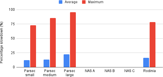
We evaluate the impact to three benchmark suites: PARSEC 3.1 [113], NAS parallel benchmarks 3.4.1 [114], and Rodinia [115]. For PARSEC, we evaluate small, medium, and large input sets. For NAS, we evaluate input sizes “A”, “B”, and “C”. For Rodinia, we use the single default input set. These benchmark suites have been widely used and contain a large variety of computation kernels that are representative of key HPC applications such as stencils, graph processing, linear algebra, computational mathematics, grid, sorting, and many others that have been observed to be important workloads in NERSC systems [116]. Overall, we use 57 CPU benchmarks for a broad representation. We use a single compute core to better focus on the effect of the additional latency to memory.
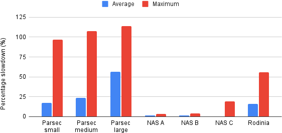
Figure 6 shows slowdown percentages for benchmarks across our three suites for an in-order core on the left and an OOO core on the right. As shown, NAS benchmarks are negligibly affected by the increased latency from photonics. Rodinia benchmarks have an average slowdown of 16% for both in-order and OOO cores. Benchmark NW shows the largest slowdown of approximately 79% for in-order cores and 55% for OOO cores. For Parsec benchmarks with large inputs, the average slowdown is 23% for in-order cores and 41% for OOO cores. However, for medium inputs, those slowdowns drop to 13% and 24%, respectively, because with medium inputs more benchmarks have a working set that fits in the LLC. The overall average slowdown for Parsec across input sizes is 16% for in-order cores and 27% for OOO cores. Across all benchmarks of the three suites and input sizes, the average slowdown with in-order cores is 15% and with OOO cores 22%. These slowdowns are considerably less than the slowdowns quoted in past work for full-system disaggregation (Section II).
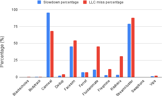
Figure 7 illustrates that the performance penalty correlates with the LLC miss rate. In fact, for Parsec with large inputs, the Pearson product-moment correlation coefficient is 0.89, while for Rodinia 0.76. For all Parsec benchmarks with small, medium, and large inputs, the coefficient is 0.822. While not shown, OOO cores show a similar behavior partly because they do not substantially change the LLC access patterns or working set sizes. In fact, for Rodinia with OOO cores, the correlation factor is 0.93, while for Parsec 0.75. All these coefficients indicate a strong correlation. In addition to LLC miss rate, the ratio of memory accesses to non-memory instructions is a key factor to an application’s slowdown; OOO cores de-emphasize this parameter slightly and stress the LLC miss rate more, as mentioned above.
Furthermore, we notice that the cycles the LLC spends in a miss increase by 50% to 150% across benchmarks for in-order and OOO cores. We further confirm the importance of LLC miss rates to performance by observing that streamcluster with small and medium inputs has an LLC miss rate of less than 0.5% and a negligible slowdown. However, streamcluster with large inputs has a working set that does not fit in the LLC, causing an LLC miss rate of over 60% and thus a slowdown of about 57%.
Focusing on the performance of individual benchmarks, for in-order cores, only three benchmarks exceed a 25% slowdown in each of Rodinia and Parsec (large) whereas for OOO cores only two benchmarks in Rodinia and three in Parsec (large). Therefore, the majority of benchmarks are impacted lightly, even without mitigation strategies. For more affected benchmarks, there is a range of mitigating hardware and software techniques [117, 118, 119, 120]. Our results motivate more memory latency-tolerant compute units for resource-disaggregated systems.
VI-B2 Sensitivity to Latency
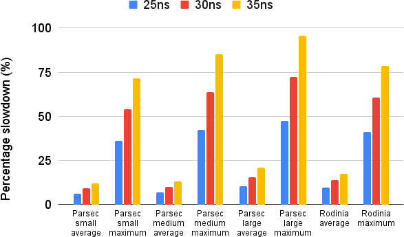
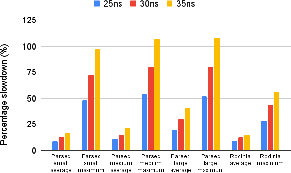
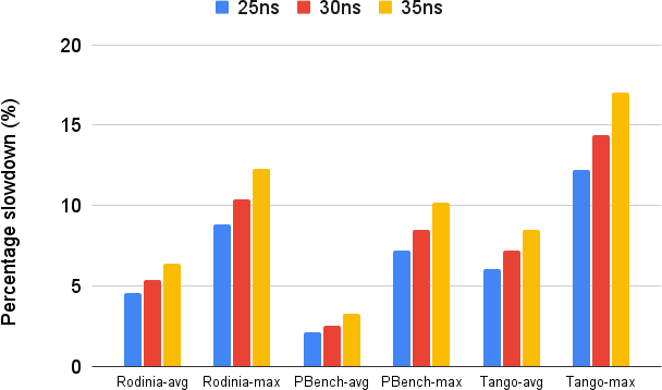
Thus far, we assumed 35 ns to cover 4 meters, which is the worst-case intra-rack distance in modern systems. Here, we assess whether improved photonics or shorter rack distances with lower latencies would greatly benefit application performance by comparing performance for 25 ns, 30 ns, and 35 ns. Results are shown in Figure 8. For both in-order and OOO cores, reducing the additional latency to 25 ns from 35 ns reduces application slowdown by about half.
VI-B3 GPU Evaluation
To evaluate the impact of the additional latency between GPUs and HBM, we extend the publicly available version of PPT-GPU [121] toolkit to account for the additional latency between the main memory of the GPU and the LLC. In our evaluation, we model one NVIDIA A100 GPU [122] running a total of 24 applications with 1525 kernels from different benchmark suites. We run 11 applications from Rodinia [115] and ten applications from Polybench [123]. Polybench applications are linear algebra applications that stress the GPU cache and main memory. Furthermore, we run AlexNet, GRU, and LSTM from the Tango deep network [124] benchmark suite. We use the default input sizes and configurations that came with the benchmarks, detailed in [121]. We run applications using the “SASS” model and extract memory and instruction traces for each application.
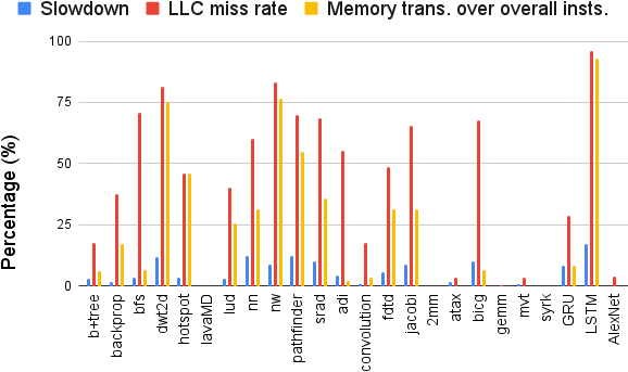
Figure 9 shows the effect of different latencies on the performance of our GPU benchmarks. We compare performance in terms of the total predicted cycles. The average slowdown across all 24 GPU applications is 5.35%. In addition, Figure 10 shows that the slowdown (shown for 35 ns) has a strong correlation with (i) the LLC miss rate and (ii) the percentage of transactions the HBM receives over the total number of instructions, indicated by a correlation factor of 0.87 and 0.79, respectively. In contrast, it has no significant correlation with the percentage of memory request instructions over the total number of instructions because the caches filter a different percentage of those requests.
VI-B4 CPU–GPU Comparison
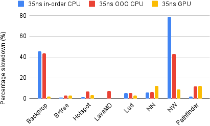
We illustrate the difference in memory latency tolerance of in-order CPUs, OOO CPUs, and GPUs in Figure 11 for the intersection of Rodinia benchmarks that correctly complete on both CPUs and GPUs with their default input sets. As shown, GPUs tolerate the additional 35 ns latency better with a maximum slowdown of 12%. This is promising for resource disaggregation given the steady growth of GPUs in HPC systems.
VI-C Power Overhead
We calculate the per-rack power overhead of our photonic solution for 350 MCMs with 2048 escape wavelengths from each MCM and 25 Gbps per wavelength. If we use demonstrated comb laser transceiver pairs that consume approximately 0.5 pJ/bit including laser power [125, 126], and include the switches of Table II that consume in total for all parallel switches no more than 1 kW, the total additional power for all photonic components is approximately 11 kW. Our analysis pessimistically assumes photonic components are constantly on. Considering that the power consumption of an A100 GPU is approximately 300 W, an AMD Milan CPU 250 W, and 512 GB of DDR4 memory in a single node approximately 192 W, the power overhead for our photonic solution is approximately 5%.
VI-D Comparison With Electronic Switches
The electronic SERDES signaling rate per wire is only 112 Gbps for a short reach. Also, typical CXL or PCIe signaling rates top out at 35 GHz/wire. In fact, as SERDES rates increase, the distance that those signals can reach reduces to even a few millimeters due to the resistance and capacitance of copper wires. Photonics break the reach limitations of copper and, with co-packaging, can achieve 4 Tbps per mm of shoreline on the chip die.
Focusing on electronic switches, Rosetta [127] and Infiniband [128] have a measured per hop latency of no less than approximately 200 ns. Emerging PCIe Gen5 switches add just 10 ns per hop [129], but only support 100 lanes per switch. To fully connect our disaggregated rack, we consider a two-level tree network with four hops (the top level is composed of an internal two-hop subnetwork). These four hops will be in addition to the 35 ns we previously evaluated for FEC and propagation (propagation delay is comparable between copper and photonic for intra-rack distances), since our photonic solution uses switches with negligible traversal latency. Therefore, the additional latency for disaggregation in the PCIe case becomes 85 ns compared to 35 ns for our photonic architecture. Finally, we also consider the latency through one hop of an Anton 3 network, which is approximately 90 ns by average [130], though scaling up to match our rack size would require multiple hops. These latencies are optimistic thus favorable for electronic switches considering that recent small-group prototypes using CXL report a minimum of 142 ns latency [26]. Scheduler decisions or congestion can cause higher worst-case (tail) latencies that may further penalize application performance. This assumes that we connect only one lane per endpoint, which carries 32 Gbps for PCIe Gen5 and 29 Gbps for Anton 3. This is multiple times less than the per-chip bandwidth of our photonic architecture.
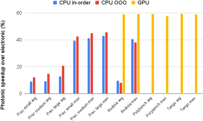
Figure 12 shows the speedup of a system that implements intra-rack disaggregation with emerging photonics with an additional 35 ns latency to and from DDR4 and HBM memory compared to a similar system that uses modern electronic switches instead. 85 ns is currently the lowest latency for electronic switches and corresponds to a four-hop PCIe Gen5 network or a single-hop Anton 3 network. As shown, for CPU benchmarks, if we only take into account “medium” from PARSEC to avoid counting PARSEC benchmarks three times, the average speedup for in-order cores is 9% and the maximum 41%. For OOO compute cores, the average is 15% and the maximum 45%. We notice that electronic switches increase the LLC’s total miss cycles by approximately 100% to 150%. For GPUs, the average and maximum are both 61%. These results show that the reduced latency of photonics compared to electronic switches has a significant application impact, making disaggregation with photonics more attractive.
VI-E Iso-Performance Comparison
Based on our performance evaluations, we estimate that in order to preserve system-wide average computational throughput as our baseline GPU-accelerated HPE/Cray EX system [29], our photonically-disaggregated system requires 6% more GPUs and 15% more CPUs, assuming in-order CPUs which is the worst case. However, intra-rack resource disaggregation allows our rack to have an average 4 fewer memory modules and 2 fewer NICs [15]. Combining the two effects, our disaggregated rack has 1075 total modules compared to 1920 in the equal-performance baseline system, an approximately 44% reduction. With such a reduction, the reduced overhead for power distribution and cooling more than compensates for the negligible power increase from photonics. Alternatively, we can preserve all rack resources and instead add 128 of a combination of CPUs and GPUs (with their HBMs), which is only an approximately 7% chip increase compared to a rack of the baseline system. Doing so doubles computational throughput.
VII Discussion
Our study highlights that more latency-tolerant CPUs [131] and GPUs [132] would make resource disaggregation more attractive. This insight is also important for systems with compute accelerators and FPGAs. FPGAs can better tolerate memory latency by customizing their compute logic [133], prefetching [134], multithreading [135], and burst scheduling [136]. Accelerators can use customized prefetching [137, 138] and other techniques [139, 140, 141].
While Perlmutter is a top HPC system, other systems should repeat our analysis to design their disaggregation hardware. Chips with higher escape bandwidths motivate fewer chips per MCM and more parallel AWGRs, but do not increase chip-to-chip photonic latency. The diversity of bottlenecks in HPC applications is a motivating argument for resource disaggregation that provides the ability to change the balance of node resources and thus support the diversity of scenarios that are typically present in a mixed-workload system.
VIII Conclusion
We discuss a resource-disaggregated HPC rack that uses modern photonic links and switches to meet BER and bandwidth requirements of HPC applications, has just a 5% power overhead, uses distributed indirect routing, is faster than an equivalent architecture with electronic switches, and allows an iso-performance system to have 44% fewer chips.
Acknowledgments
This work was supported by ARPA-E ENLITENED Program (project award DE-AR00000843) and the Director, Office of Science, of the U.S. Department of Energy under Contract No. DE-AC02-05CH11231.
References
- [1] B. Liu, D. Zydek, H. Selvaraj, and L. Gewali, “Accelerating high performance computing applications: Using cpus, gpus, hybrid CPU/GPU, and fpgas,” in 2012 13th International Conference on Parallel and Distributed Computing, Applications and Technologies, 2012, pp. 337–342.
- [2] (2018, November) The top500 HPC list. [Online]. Available: https://www.top500.org/green500/lists/2018/11/
- [3] M. Ujaldón, “Hpc accelerators with 3d memory,” in 2016 IEEE Intl Conference on Computational Science and Engineering (CSE) and IEEE Intl Conference on Embedded and Ubiquitous Computing (EUC) and 15th Intl Symposium on Distributed Computing and Applications for Business Engineering (DCABES), 2016, pp. 320–328.
- [4] S. Mittal and J. S. Vetter, “A survey of cpu-gpu heterogeneous computing techniques,” ACM Comput. Surv., vol. 47, no. 4, Jul. 2015.
- [5] D. Tiwari, S. Gupta, J. Rogers, D. Maxwell, P. Rech, S. Vazhkudai, D. Oliveira, D. Londo, N. DeBardeleben, P. Navaux, L. Carro, and A. Bland, “Understanding gpu errors on large-scale hpc systems and the implications for system design and operation,” in 2015 IEEE 21st International Symposium on High Performance Computer Architecture (HPCA), 2015, pp. 331–342.
- [6] Y. Gao and P. Zhang, “A survey of homogeneous and heterogeneous system architectures in high performance computing,” in 2016 IEEE International Conference on Smart Cloud (SmartCloud), 2016, pp. 170–175.
- [7] D. Milojicic, “Accelerators for artificial intelligence and high-performance computing,” Computer, vol. 53, no. 2, pp. 14–22, 2020.
- [8] H. Asaadi and B. Chapman, “Comparative study of deep learning framework in hpc environments,” in 2017 New York Scientific Data Summit (NYSDS), 2017, pp. 1–7.
- [9] O. Segal, N. Nasiri, M. Margala, and W. Vanderbauwhede, “High level programming of FPGAs for HPC and data centric applications,” in 2014 IEEE High Performance Extreme Computing Conference (HPEC), 2014, pp. 1–3.
- [10] T. Hogervorst, T. D. Qiu, G. Marchiori, A. Birger, M. Blatt, and R. Nane, “Hardware acceleration of HPC computational flow dynamics using HBM-enabled FPGAs,” 2021.
- [11] J. Lant, J. Navaridas, M. Luján, and J. Goodacre, “Toward fpga-based HPC: Advancing interconnect technologies,” IEEE Micro, vol. 40, no. 1, pp. 25–34, 2020.
- [12] R. Dimond, S. Racanière, and O. Pell, “Accelerating large-scale hpc applications using fpgas,” in 2011 IEEE 20th Symposium on Computer Arithmetic, 2011, pp. 191–192.
- [13] G. Ramirez-Gargallo, M. Garcia-Gasulla, and F. Mantovani, “Tensorflow on state-of-the-art HPC clusters: A machine learning use case,” in 2019 19th IEEE/ACM International Symposium on Cluster, Cloud and Grid Computing (CCGRID), 2019, pp. 526–533.
- [14] M. G. Venkata, F. Aderholdt, and Z. Parchman, “SharP: Towards programming extreme-scale systems with hierarchical heterogeneous memory,” in 2017 46th International Conference on Parallel Processing Workshops (ICPPW), 2017, pp. 145–154.
- [15] G. Michelogiannakis, B. Klenk, B. Cook, M. Y. Teh, M. Glick, L. Dennison, K. Bergman, and J. Shalf, “A case for intra-rack resource disaggregation in HPC,” ACM Trans. Archit. Code Optim., jan 2022, just Accepted.
- [16] G. P. Rodrigo, P. Östberg, E. Elmroth, K. Antypas, R. Gerber, and L. Ramakrishnan, “Towards understanding job heterogeneity in hpc: A nersc case study,” in 2016 16th IEEE/ACM International Symposium on Cluster, Cloud and Grid Computing (CCGrid), 2016, pp. 521–526.
- [17] A. Guleria, J. Lakshmi, and C. Padala, “Quadd: Quantifying accelerator disaggregated datacenter efficiency,” in 2019 IEEE 12th International Conference on Cloud Computing (CLOUD), 2019, pp. 349–357.
- [18] I. Peng, R. Pearce, and M. Gokhale, “On the memory underutilization: Exploring disaggregated memory on HPC systems,” in 2020 IEEE 32nd International Symposium on Computer Architecture and High Performance Computing (SBAC-PAD), 2020, pp. 183–190.
- [19] J. Taylor, “Facebook’s data center infrastructure: Open compute, disaggregated rack, and beyond,” in 2015 Optical Fiber Communications Conference and Exhibition (OFC), 2015, pp. 1–1.
- [20] H. Li, D. S. Berger, S. Novakovic, L. Hsu, D. Ernst, P. Zardoshti, M. Shah, I. Agarwal, M. D. Hill, M. Fontoura, and R. Bianchini, “First-generation memory disaggregation for cloud platforms.” arXiv, 2022.
- [21] K. Koh, K. Kim, S. Jeon, and J. Huh, “Disaggregated cloud memory with elastic block management,” IEEE Transactions on Computers, vol. 68, no. 1, pp. 39–52, 2019.
- [22] A. D. Papaioannou, R. Nejabati, and D. Simeonidou, “The benefits of a disaggregated data centre: A resource allocation approach,” in 2016 IEEE Global Communications Conference (GLOBECOM), 2016, pp. 1–7.
- [23] J. Gonzalez, A. Gazman, M. Hattink, M. G. Palma, M. Bahadori, R. Rubio-Noriega, L. Orosa, M. Glick, O. Mutlu, K. Bergman, and R. Azevedo, “Optically connected memory for disaggregated data centers,” in 2020 IEEE 32nd International Symposium on Computer Architecture and High Performance Computing (SBAC-PAD), 2020, pp. 43–50.
- [24] Q. Cheng, K. Bergman, Y. Huang, H. Yang, M. Bahadori, N. Abrams, X. Meng, M. Glick, Y. Liu, and M. Hochberg, “Silicon photonic switch topologies and routing strategies for disaggregated data centers,” IEEE Journal of Selected Topics in Quantum Electronics, vol. PP, pp. 1–1, 12 2019.
- [25] A. Guleria, J. Lakshmi, and C. Padala, “Emf: Disaggregated gpus in datacenters for efficiency, modularity and flexibility,” in 2019 IEEE International Conference on Cloud Computing in Emerging Markets (CCEM), 2019, pp. 1–8.
- [26] H. Li, D. S. Berger, L. Hsu, D. Ernst, P. Zardoshti, S. Novakovic, M. Shah, S. Rajadnya, S. Lee, I. Agarwal, M. D. Hill, M. Fontoura, and R. Bianchini, “Pond: CXL-based memory pooling systems for cloud platforms,” in Proceedings of the 28th ACM International Conference on Architectural Support for Programming Languages and Operating Systems, Volume 2, ser. ASPLOS 2023. New York, NY, USA: Association for Computing Machinery, 2023, p. 574–587. [Online]. Available: https://doi.org/10.1145/3575693.3578835
- [27] H. A. Maruf, H. Wang, A. Dhanotia, J. Weiner, N. Agarwal, P. Bhattacharya, C. Petersen, M. Chowdhury, S. Kanaujia, and P. Chauhan, “TPP: Transparent page placement for CXL-enabled tiered-memory,” in Proceedings of the 28th ACM International Conference on Architectural Support for Programming Languages and Operating Systems, Volume 3, ser. ASPLOS 2023. New York, NY, USA: Association for Computing Machinery, 2023, p. 742–755. [Online]. Available: https://doi.org/10.1145/3582016.3582063
- [28] P. Duraisamy, W. Xu, S. Hare, R. Rajwar, D. Culler, Z. Xu, J. Fan, C. Kennelly, B. McCloskey, D. Mijailovic, B. Morris, C. Mukherjee, J. Ren, G. Thelen, P. Turner, C. Villavieja, P. Ranganathan, and A. Vahdat, “Towards an adaptable systems architecture for memory tiering at warehouse-scale,” in Proceedings of the 28th ACM International Conference on Architectural Support for Programming Languages and Operating Systems, Volume 3, ser. ASPLOS 2023. New York, NY, USA: Association for Computing Machinery, 2023, p. 727–741. [Online]. Available: https://doi.org/10.1145/3582016.3582031
- [29] NERSC’s Perlmutter configuration. [Online]. Available: https://docs.nersc.gov/systems/perlmutter/
- [30] T. K. Petersen and J. Bent, “Hybrid flash arrays for hpc storage systems: An alternative to burst buffers,” in 2017 IEEE High Performance Extreme Computing Conference (HPEC), 2017, pp. 1–7.
- [31] M. Glick, N. C. Abrams, Q. Cheng, M. Y. Teh, Y. H. Hung, O. Jimenez, S. Liu, Y. Okawachi, X. Meng, L. Johansson, M. Ghobadi, L. Dennison, G. Michelogiannakis, J. Shalf, A. Liu, J. Bowers, A. Gaeta, M. Lipson, and K. Bergman, “PINE: Photonic integrated networked energy efficient datacenters (enlitened program) [invited],” IEEE/OSA Journal of Optical Communications and Networking, vol. 12, no. 12, pp. 443–456, 2020.
- [32] X. Guo, X. Xue, B. Pan, F. Yan, G. Exarchakos, and N. Calabretta, “Fosda: A hybrid disaggregated hpc architecture based on distributed nanoseconds optical switches,” in Future computing, 2021.
- [33] R. Lin, Y. Cheng, M. D. Andrade, L. Wosinska, and J. Chen, “Disaggregated data centers: Challenges and trade-offs,” IEEE Communications Magazine, vol. 58, no. 2, 2020.
- [34] A. Call, J. Polo, D. Carrera, F. Guim, and S. Sen, “Disaggregating non-volatile memory for throughput-oriented genomics workloads,” CoRR, vol. abs/2007.02813, 2020.
- [35] G. Liu, R. Proietti, M. Fariborz, P. Fotouhi, X. Xiao, and S. J. B. Yoo, “Architecture and performance studies of 3d-hyper-flex-lion for reconfigurable all-to-all hpc networks,” in Proceedings of the International Conference for High Performance Computing, Networking, Storage and Analysis, ser. SC ’20. IEEE Press, 2020.
- [36] Y. Zhang, X. Xiao, K. Zhang, S. Li, A. Samanta, Y. Zhang, K. Shang, R. Proietti, K. Okamoto, and S. J. B. Yoo, “Foundry-enabled scalable all-to-all optical interconnects using silicon nitride arrayed waveguide router interposers and silicon photonic transceivers,” IEEE Journal of Selected Topics in Quantum Electronics, vol. 25, no. 5, pp. 1–9, 2019.
- [37] T. J. Seok, K. Kwon, J. Henriksson, J. Luo, and M. C. Wu, “Wafer-scale silicon photonic switches beyond die size limit,” Optica, vol. 6, no. 4, pp. 490–494, Apr 2019. [Online]. Available: http://opg.optica.org/optica/abstract.cfm?URI=optica-6-4-490
- [38] Y. Ding, V. Kamchevska, K. Dalgaard, F. Ye, R. Asif, S. Gross, M. Withford, M. Galili, T. Morioka, and L. Oxenlowe, “Reconfigurable sdm switching using novel silicon photonic integrated circuit,” Scientific Reports, vol. 6, 08 2016.
- [39] Y. Huang, Q. Cheng, A. Rizzo, and K. Bergman, “Push—pull microring-assisted space-and-wavelength selective switch,” Opt. Lett., vol. 45, no. 10, pp. 2696–2699, May 2020.
- [40] K. Lim, J. Chang, T. Mudge, P. Ranganathan, S. K. Reinhardt, and T. F. Wenisch, “Disaggregated memory for expansion and sharing in blade servers,” SIGARCH Comput. Archit. News, vol. 37, no. 3, p. 267–278, jun 2009.
- [41] S. Van Doren, “Abstract - hoti 2019: Compute express link,” in 2019 IEEE Symposium on High-Performance Interconnects (HOTI), 2019, pp. 18–18.
- [42] G. Zervas, H. Yuan, A. Saljoghei, Q. Chen, and V. Mishra, “Optically disaggregated data centers with minimal remote memory latency: Technologies, architectures, and resource allocation [invited],” IEEE/OSA Journal of Optical Communications and Networking, vol. 10, no. 2, pp. A270–A285, 2018.
- [43] P. X. Gao, A. Narayan, S. Karandikar, J. Carreira, S. Han, R. Agarwal, S. Ratnasamy, and S. Shenker, “Network requirements for resource disaggregation,” in Proceedings of the 12th USENIX Conference on Operating Systems Design and Implementation, ser. OSDI’16. USENIX Association, 2016.
- [44] B. Abali, R. J. Eickemeyer, H. Franke, C.-S. Li, and M. A. Taubenblatt, “Disaggregated and optically interconnected memory: when will it be cost effective?” 2015.
- [45] S. Han, N. Egi, A. Panda, S. Ratnasamy, G. Shi, and S. Shenker, “Network support for resource disaggregation in next-generation datacenters,” in Proceedings of the Twelfth ACM Workshop on Hot Topics in Networks, ser. HotNets-XII, 2013.
- [46] Y. Cheng, M. De Andrade, L. Wosinska, and J. Chen, “Resource disaggregation versus integrated servers in data centers: Impact of internal transmission capacity limitation,” in 2018 European Conference on Optical Communication (ECOC), 2018, pp. 1–3.
- [47] Y. Fan, Z. Lan, P. Rich, W. E. Allcock, M. E. Papka, B. Austin, and D. Paul, “Scheduling beyond CPUs for HPC,” Proceedings of the 28th International Symposium on High-Performance Parallel and Distributed Computing, Jun 2019.
- [48] G. Agosta, W. Fornaciari, G. Massari, A. Pupykina, F. Reghenzani, and M. Zanella, “Managing heterogeneous resources in HPC systems,” ser. PARMA-DITAM ’18. New York, NY, USA: Association for Computing Machinery, 2018, p. 7–12.
- [49] M. Amaral, J. Polo, D. Carrera, N. Gonzalez, C.-C. Yang, A. Morari, B. D’Amora, A. Youssef, and M. Steinder, “DRMaestro: orchestrating disaggregated resources on virtualized data-centers,” Journal of Cloud Computing, vol. 10, 03 2021.
- [50] G. Domeniconi, E. Lee, V. Venkataswamy, and S. Dola, “CuSH: Cognitive scheduler for heterogeneous high performance computing system,” 2019.
- [51] A. B. Maccabe, “Operating and runtime systems challenges for hpc systems,” in Proceedings of the 7th International Workshop on Runtime and Operating Systems for Supercomputers ROSS 2017, ser. ROSS ’17, 2017.
- [52] W. Hwu, L. Chang, H. Kim, A. Dakkak, and I. El Hajj, “Transitioning hpc software to exascale heterogeneous computing,” in 2015 Computational Electromagnetics International Workshop (CEM), 2015, pp. 1–2.
- [53] Y. Shan, Y. Huang, Y. Chen, and Y. Zhang, “Legoos: A disseminated, distributed os for hardware resource disaggregation,” in Proceedings of the 13th USENIX Conference on Operating Systems Design and Implementation, ser. OSDI’18. USENIX Association, 2018, p. 69–87.
- [54] R. Gioiosa, O. B. Mutlu, S. Lee, S. J. Vetter, G. Picierro, and M. Cesati, “The minos computing library - efficient parallel programming for extremely heterogeneous systems,” GPGPU@PPoPP, pp. 1–10, 2020.
- [55] H. Khaleghzadeh, R. R. Manumachu, and A. Lastovetsky, “A hierarchical data-partitioning algorithm for performance optimization of data-parallel applications on heterogeneous multi-accelerator numa nodes,” IEEE Access, vol. 8, pp. 7861–7876, 2020.
- [56] Z. Hussain, “Heterogeneity aware fault tolerance for extreme scale computing,” August 2020. [Online]. Available: http://d-scholarship.pitt.edu/39456/
- [57] P. Jamieson, A. Sanaullah, and M. Herbordt, “Benchmarking heterogeneous hpc systems including reconfigurable fabrics: Community aspirations for ideal comparisons,” in 2018 IEEE High Performance extreme Computing Conference (HPEC), 2018, pp. 1–6.
- [58] K. Tang, D. Tiwari, S. Gupta, S. S. Vazhkudai, and X. He, “Effective running of end-to-end hpc workflows on emerging heterogeneous architectures,” in 2017 IEEE International Conference on Cluster Computing (CLUSTER), 2017, pp. 344–348.
- [59] A. Lastovetsky, “Heterogeneous parallel computing: from clusters of workstations to hierarchical hybrid platforms,” Supercomputing Frontiers and Innovations, vol. 1, no. 3, 2015.
- [60] J. Guo, Z. Chang, S. Wang, H. Ding, Y. Feng, L. Mao, and Y. Bao, “Who limits the resource efficiency of my datacenter: An analysis of alibaba datacenter traces,” in Proceedings of the International Symposium on Quality of Service, ser. IWQoS ’19, 2019.
- [61] J. Patel, V. Jindal, I. Yen, F. Bastani, J. Xu, and P. Garraghan, “Workload estimation for improving resource management decisions in the cloud,” in 2015 IEEE Twelfth International Symposium on Autonomous Decentralized Systems, 2015, pp. 25–32.
- [62] T. Li, V. K. Narayana, and T. A. El-Ghazawi, “Efficient resource sharing through GPU virtualization on accelerated high performance computing systems,” CoRR, vol. abs/1511.07658, 2015.
- [63] M. Jeon, S. Venkataraman, A. Phanishayee, u. Qian, W. Xiao, and F. Yang, “Analysis of large-scale multi-tenant gpu clusters for dnn training workloads,” in Proceedings of the 2019 USENIX Conference on Usenix Annual Technical Conference, ser. USENIX ATC ’19. USA: USENIX Association, 2019, p. 947–960.
- [64] T. Li, V. K. Narayana, E. El-Araby, and T. El-Ghazawi, “Gpu resource sharing and virtualization on high performance computing systems,” in 2011 International Conference on Parallel Processing, 2011, pp. 733–742.
- [65] N. Terzenidis, M. Moralis-Pegios, G. Mourgias-Alexandris, T. Alexoudi, K. Vyrsokinos, and N. Pleros, “High-port and low-latency optical switches for disaggregated data centers: The hipolaos switch architecture,” IEEE/OSA Journal of Optical Communications and Networking, vol. 10, no. 7, pp. 102–116, 2018.
- [66] Z. Wang, H. Huang, J. Zhang, and G. Alonso, “Benchmarking high bandwidth memory on FPGAs,” 2020.
- [67] J. Meza, Q. Wu, S. Kumar, and O. Mutlu, “Revisiting memory errors in large-scale production data centers: Analysis and modeling of new trends from the field,” in 45th Annual IEEE/IFIP International Conference on Dependable Systems and Networks, DSN 2015, Rio de Janeiro, Brazil, June 22-25, 2015. IEEE Computer Society, 2015, pp. 415–426.
- [68] V. Sridharan, N. DeBardeleben, S. Blanchard, K. B. Ferreira, J. Stearley, J. Shalf, and S. Gurumurthi, “Memory errors in modern systems: The good, the bad, and the ugly,” in Proceedings of the Twentieth International Conference on Architectural Support for Programming Languages and Operating Systems, ASPLOS ’15, Istanbul, Turkey, March 14-18, 2015, Ö. Özturk, K. Ebcioglu, and S. Dwarkadas, Eds. ACM, 2015, pp. 297–310.
- [69] S. Luyi, F. Jinyi, and Y. Xiaohua, “Forward error correction,” in 2012 Fourth International Conference on Computational and Information Sciences, 2012, pp. 37–40.
- [70] B. Y. Kim, Y. Okawachi, J. K. Jang, M. Yu, X. Ji, Y. Zhao, C. Joshi, M. Lipson, and A. L. Gaeta, “Turn-key, high-efficiency kerr comb source,” Opt. Lett., vol. 44, no. 18, pp. 4475–4478, Sep 2019.
- [71] S. Chen, S. Irving, L. Peng, Y. Hu, Y. Zhang, and A. Srivastava, “Using switchable pins to increase off-chip bandwidth in chip-multiprocessors,” IEEE Trans. Parallel Distrib. Syst., vol. 28, no. 1, p. 274–289, jan 2017.
- [72] N. P. Jouppi, C. Young, N. Patil, D. Patterson, G. Agrawal, R. Bajwa, S. Bates, S. Bhatia, N. Boden, A. Borchers, R. Boyle, P.-l. Cantin, C. Chao, C. Clark, J. Coriell, M. Daley, M. Dau, J. Dean, B. Gelb, T. V. Ghaemmaghami, R. Gottipati, W. Gulland, R. Hagmann, C. R. Ho, D. Hogberg, J. Hu, R. Hundt, D. Hurt, J. Ibarz, A. Jaffey, A. Jaworski, A. Kaplan, H. Khaitan, D. Killebrew, A. Koch, N. Kumar, S. Lacy, J. Laudon, J. Law, D. Le, C. Leary, Z. Liu, K. Lucke, A. Lundin, G. MacKean, A. Maggiore, M. Mahony, K. Miller, R. Nagarajan, R. Narayanaswami, R. Ni, K. Nix, T. Norrie, M. Omernick, N. Penukonda, A. Phelps, J. Ross, M. Ross, A. Salek, E. Samadiani, C. Severn, G. Sizikov, M. Snelham, J. Souter, D. Steinberg, A. Swing, M. Tan, G. Thorson, B. Tian, H. Toma, E. Tuttle, V. Vasudevan, R. Walter, W. Wang, E. Wilcox, and D. H. Yoon, “In-datacenter performance analysis of a tensor processing unit,” in Proceedings of the 44th Annual International Symposium on Computer Architecture, ser. ISCA ’17. New York, NY, USA: ACM, 2017, pp. 1–12.
- [73] M. Wade, “TeraPHY: A chiplet technology for low-power, high-bandwidth in-package optical i/o,” in 2019 IEEE Hot Chips 31 Symposium (HCS), 2019, pp. i–xlviii.
- [74] K. Bergman, J. Shalf, G. Michelogiannakis, S. Rumley, L. Dennison, and M. Ghobadi, “Pine: An energy efficient flexibly interconnected photonic data center architecture for extreme scalability,” in 2018 IEEE Optical Interconnects Conference (OI), 2018, pp. 25–26.
- [75] P. Maniotis, L. Schares, M. A. Taubenblatt, and D. M. Kuchta, “Co-packaged optics for HPC and data center networks,” in Optical Interconnects XXI, H. Schröder and R. T. Chen, Eds., vol. 11692, International Society for Optics and Photonics. SPIE, 2021, pp. 17 – 22.
- [76] C. Minkenberg, R. Krishnaswamy, A. Zilkie, and D. Nelson, “Co-packaged datacenter optics: Opportunities and challenges,” IET Optoelectronics, vol. 15, no. 2, pp. 77–91, 2021.
- [77] A. Sutono, A. Pham, J. Laskar, and W. Smith, “Investigations of multi-layer ceramic-based mcm technology,” in IEEE 7th Topical Meeting on Electrical Performance of Electronic Packaging (Cat. No.98TH8370), 1998, pp. 83–86.
- [78] N. C. Abrams, Q. Cheng, M. Glick, M. Jezzini, P. Morrissey, P. O’Brien, and K. Bergman, “Silicon photonic 2.5d multi-chip module transceiver for high-performance data centers,” Journal of Lightwave Technology, vol. 38, no. 13, pp. 3346–3357, 2020.
- [79] M. Dittrich, A. Heinig, F. Hopsch, and R. Trieb, “Heterogeneous interposer based integration of chips with copper pillars and c4 balls to achieve high speed interfaces for adc application,” in 2017 IEEE 67th Electronic Components and Technology Conference (ECTC), 2017, pp. 643–648.
- [80] S. Fathololoumi, D. Hui, S. Jadhav, J. Chen, K. Nguyen, M. N. Sakib, Z. Li, H. Mahalingam, S. Amiralizadeh, N. N. Tang, H. Potluri, M. Montazeri, H. Frish, R. A. Defrees, C. Seibert, A. Krichevsky, J. K. Doylend, J. Heck, R. Venables, A. Dahal, A. Awujoola, A. Vardapetyan, G. Kaur, M. Cen, V. Kulkarni, S. S. Islam, R. L. Spreitzer, S. Garag, A. C. Alduino, R. Chiou, L. Kamyab, S. Gupta, B. Xie, R. S. Appleton, S. Hollingsworth, S. McCargar, Y. Akulova, K. M. Brown, R. Jones, D. Zhu, T. Liljeberg, and L. Liao, “1.6 tbps silicon photonics integrated circuit and 800 gbps photonic engine for switch co-packaging demonstration,” Journal of Lightwave Technology, vol. 39, no. 4, pp. 1155–1161, 2021.
- [81] E. Agrell, M. Karlsson, A. R. Chraplyvy, D. J. Richardson, P. M. Krummrich, P. Winzer, K. Roberts, J. K. Fischer, S. J. Savory, B. J. Eggleton, M. Secondini, F. R. Kschischang, A. Lord, J. Prat, I. Tomkos, J. E. Bowers, S. Srinivasan, M. Brandt-Pearce, and N. Gisin, “Roadmap of optical communications,” Journal of Optics, vol. 18, no. 6, p. 063002, may 2016.
- [82] J. Wei, Q. Cheng, R. V. Penty, I. H. White, and D. G. Cunningham, “400 gigabit ethernet using advanced modulation formats: Performance, complexity, and power dissipation,” IEEE Communications Magazine, vol. 53, no. 2, pp. 182–189, 2015.
- [83] B. Y. Kim, Y. Okawachi, J. K. Jang, M. Yu, X. Ji, Y. Zhao, C. Joshi, M. Lipson, and A. L. Gaeta, “Turn-key, high-efficiency kerr comb source,” Opt. Lett., vol. 44, no. 18, pp. 4475–4478, Sep 2019.
- [84] D. D. Sharma, “Pci express® 6.0 specification at 64.0 gt/s with pam-4 signaling: a low latency, high bandwidth, high reliability and cost-effective interconnect,” in 2020 IEEE Symposium on High-Performance Interconnects (HOTI), 2020, pp. 1–8.
- [85] K. Ikeda, K. Suzuki, R. Konoike, S. Namiki, and H. Kawashima, “Large-scale silicon photonics switch based on 45-nm cmos technology,” Optics Communications, vol. 466, p. 125677, 2020.
- [86] T. J. Seok, K. Kwon, J. Henriksson, J. Luo, and M. C. Wu, “240×240 wafer-scale silicon photonic switches,” in 2019 Optical Fiber Communications Conference and Exhibition (OFC), 2019, pp. 1–3.
- [87] A. S. P. Khope, A. M. Netherton, T. Hirokawa, N. Volet, E. J. Stanton, C. Schow, R. Helkey, A. A. M. Saleh, J. E. Bowers, and R. C. Alferness, “Elastic wdm optoelectronic crossbar switch with on-chip wavelength control,” in Advanced Photonics 2017 (IPR, NOMA, Sensors, Networks, SPPCom, PS). Optica Publishing Group, 2017, p. PTh1D.3.
- [88] Q. Cheng, M. Bahadori, Y.-H. Hung, Y. Huang, N. Abrams, and K. Bergman, “Scalable microring-based silicon clos switch fabric with switch-and-select stages,” IEEE Journal of Selected Topics in Quantum Electronics, vol. 25, no. 5, pp. 1–11, 2019.
- [89] K.-i. Sato, “Realization and Application of Large-Scale Fast Optical Circuit Switch for Data Center Networking,” Journal of Lightwave Technology, vol. 36, no. 7, pp. 1411–1419, Apr. 2018.
- [90] S series optical circuit switch. [Online]. Available: https://www.calient.net/products/s-series-photonic-switch/
- [91] D. Nikolova, D. M. Calhoun, Y. Liu, S. Rumley, A. Novack, T. Baehr-Jones, M. Hochberg, and K. Bergman, “Modular architecture for fully non-blocking silicon photonic switch fabric,” Microsystems & nanoengineering, vol. 3, no. 1, pp. 1–9, 2017.
- [92] L. Y. Dai, Y.-H. Hung, Q. Cheng, and K. Bergman, “Experimental demonstration of pam-4 transmission through microring silicon photonic clos switch fabric,” in 2020 Optical Fiber Communications Conference and Exhibition (OFC), 2020, pp. 1–3.
- [93] R. Proietti, Y. Yin, R. Yu, C. J. Nitta, V. Akella, C. Mineo, and S. J. B. Yoo, “Scalable optical interconnect architecture using awgr-based tonak lion switch with limited number of wavelengths,” Journal of Lightwave Technology, vol. 31, no. 24, pp. 4087–4097, 2013.
- [94] C. Lea, “A scalable awgr-based optical switch,” Journal of Lightwave Technology, vol. 33, no. 22, pp. 4612–4621, Nov 2015.
- [95] Dhoore, Sören and Roelkens, Günther and Morthier, Geert, “Fast wavelength-tunable lasers on silicon,” IEEE JOURNAL OF SELECTED TOPICS IN QUANTUM ELECTRONICS, vol. 25, no. 6, pp. 1 500 908:1–1 500 908:8, 2019.
- [96] “Optical circuit switch product availability,” https://www.fs.com/products/66601.html.
- [97] K.-i. Sato, H. Hasegawa, T. Niwa, and T. Watanabe, “A large-scale wavelength routing optical switch for data center networks,” IEEE Communications Magazine, vol. 51, no. 9, pp. 46–52, Sep. 2013.
- [98] K. Ueda, Y. Mori, H. Hasegawa, H. Matsuura, K. Ishii, H. Kuwatsuka, S. Namiki, T. Watanabe, and K.-i. Sato, “Demonstration of 1,440×1,440 fast optical circuit switch for datacenter networking,” in 2016 21st OptoElectronics and Communications Conference (OECC) Held Jointly with 2016 International Conference on Photonics in Switching (PS), Jul. 2016, pp. 1–3.
- [99] S. Bhoja, “Pam4 signaling for intra-data center and data center to data center connectivity (dci),” in 2017 Optical Fiber Communications Conference and Exhibition (OFC), 2017, pp. 1–54.
- [100] D. M. Marom, P. D. Colbourne, A. D’errico, N. K. Fontaine, Y. Ikuma, R. Proietti, L. Zong, J. M. Rivas-Moscoso, and I. Tomkos, “Survey of photonic switching architectures and technologies in support of spatially and spectrally flexible optical networking [invited],” IEEE/OSA Journal of Optical Communications and Networking, vol. 9, no. 1, pp. 1–26, 2017.
- [101] M. Y. Teh, Y.-H. Hung, G. Michelogiannakis, S. Yan, M. Glick, J. Shalf, and K. Bergman, “Tago: Rethinking routing design in high performance reconfigurable networks,” in SC20: International Conference for High Performance Computing, Networking, Storage and Analysis, 2020, pp. 1–16.
- [102] G. Michelogiannakis, Y. Shen, M. Y. Teh, X. Meng, B. Aivazi, T. Groves, J. Shalf, M. Glick, M. Ghobadi, L. Dennison, and K. Bergman, “Bandwidth steering in HPC using silicon nanophotonics,” in Proceedings of the International Conference for High Performance Computing, Networking, Storage and Analysis, ser. SC ’19, 2019.
- [103] J. Shalf, S. Kamil, L. Oliker, and D. Skinner, “Analyzing ultra-scale application communication requirements for a reconfigurable hybrid interconnect,” in Proceedings of the ACM/IEEE SC2005 Conference on High Performance Networking and Computing, November 12-18, 2005, Seattle, WA, USA, CD-Rom, 2005, p. 17.
- [104] J. S. Vetter and F. Mueller, “Communication characteristics of large-scale scientific applications for contemporary cluster architectures,” in 16th International Parallel and Distributed Processing Symposium (IPDPS 2002), 15-19 April 2002, Fort Lauderdale, FL, USA, CD-ROM/Abstracts Proceedings, 2002.
- [105] J. Domke, S. Matsuoka, I. R. Ivanov, Y. Tsushima, T. Yuki, A. Nomura, S. Miura, N. McDonald, D. L. Floyd, and N. Dubé, “Hyperx topology: First at-scale implementation and comparison to the fat-tree,” in Proceedings of the International Conference for High Performance Computing, Networking, Storage and Analysis, ser. SC ’19, 2019.
- [106] S. Ma, Z. Wang, N. Enright Jerger, L. Shen, and N. Xiao, “Novel flow control for fully adaptive routing in cache-coherent nocs,” IEEE Transactions on Parallel and Distributed Systems, vol. 25, no. 9, pp. 2397–2407, 2014.
- [107] D. U. Becker and W. J. Dally, “Allocator implementations for network-on-chip routers,” in Proceedings of the Conference on High Performance Computing Networking, Storage and Analysis, 2009, pp. 1–12.
- [108] N. Jiang, J. Kim, and W. J. Dally, “Indirect adaptive routing on large scale interconnection networks,” in Proceedings of the 36th Annual International Symposium on Computer Architecture, ser. ISCA ’09, 2009, pp. 220–231.
- [109] D. De Sensi, S. Di Girolamo, K. H. McMahon, D. Roweth, and T. Hoefler, “An in-depth analysis of the slingshot interconnect,” in SC20: International Conference for High Performance Computing, Networking, Storage and Analysis, 2020, pp. 1–14.
- [110] K. Hosseini, E. Kok, S. Y. Shumarayev, C.-P. Chiu, A. Sarkar, A. Toda, Y. Ke, A. Chan, D. Jeong, M. Zhang, S. Raman, T. Tran, K. A. Singh, P. Bhargava, C. Zhang, H. Lu, R. Mahajan, X. Li, N. Deshpande, C. O’Keeffe, T. T. Hoang, U. Krishnamoorthy, C. Sun, R. Meade, V. Stojanovic, and M. Wade, “8 tbps co-packaged FPGA and silicon photonics optical IO,” in 2021 Optical Fiber Communications Conference and Exhibition (OFC), 2021, pp. 1–3.
- [111] H. Yang, V. Akella, C.-N. Chuah, and S. Yoo, “Scheduling optical packets in wavelength, time, and space domains for all-optical packet switching routers,” in IEEE International Conference on Communications, 2005. ICC 2005. 2005, vol. 3, 2005, pp. 1836–1842 Vol. 3.
- [112] N. Binkert, B. Beckmann, G. Black, S. K. Reinhardt, A. Saidi, A. Basu, J. Hestness, D. R. Hower, T. Krishna, S. Sardashti, R. Sen, K. Sewell, M. Shoaib, N. Vaish, M. D. Hill, and D. A. Wood, “The gem5 simulator,” SIGARCH Comput. Archit. News, vol. 39, no. 2, p. 1–7, aug 2011.
- [113] C. Bienia, S. Kumar, J. P. Singh, and K. Li, “The parsec benchmark suite: Characterization and architectural implications,” in 2008 International Conference on Parallel Architectures and Compilation Techniques (PACT), 2008, pp. 72–81.
- [114] D. Bailey, E. Barszcz, L. Dagum, and H. Simon, “Nas parallel benchmark results,” in Supercomputing ’92:Proceedings of the 1992 ACM/IEEE Conference on Supercomputing, 1992, pp. 386–393.
- [115] S. Che, M. Boyer, J. Meng, D. Tarjan, J. W. Sheaffer, S.-H. Lee, and K. Skadron, “Rodinia: A benchmark suite for heterogeneous computing,” in 2009 IEEE International Symposium on Workload Characterization (IISWC), 2009, pp. 44–54.
- [116] NERSC-10 workload analysis (data from 2018).
- [117] O. Mutlu, H. Kim, and Y. Patt, “Efficient runahead execution: Power-efficient memory latency tolerance,” IEEE Micro, vol. 26, no. 1, pp. 10–20, 2006.
- [118] J.-M. Parcerisa and A. Gonzalez, “Improving latency tolerance of multithreading through decoupling,” IEEE Transactions on Computers, vol. 50, no. 10, pp. 1084–1094, 2001.
- [119] T. Mowry, C. Chan, and A. Lo, “Comparative evaluation of latency tolerance techniques for software distributed shared memory,” in Proceedings 1998 Fourth International Symposium on High-Performance Computer Architecture, 1998, pp. 300–311.
- [120] S. Nekkalapu, H. Akkary, K. Jothi, R. Retnamma, and X. Song, “A simple latency tolerant processor,” in 2008 IEEE International Conference on Computer Design, 2008, pp. 384–389.
- [121] Y. Arafa, A.-H. Badawy, A. ElWazir, A. Barai, A. Eker, G. Chennupati, N. Santhi, and S. Eidenbenz, “Hybrid, scalable, trace-driven performance modeling of GPGPUs,” in Proceedings of the International Conference for High Performance Computing, Networking, Storage and Analysis, ser. SC ’21, 2021.
- [122] J. Choquette and W. Gandhi, “NVIDIA A100 GPU: Performance & innovation for GPU computing,” in 2020 IEEE Hot Chips 32 Symposium (HCS), 2020, pp. 1–43.
- [123] S. Grauer-Gray, L. Xu, R. Searles, S. Ayalasomayajula, and J. Cavazos, “Auto-tuning a high-level language targeted to gpu codes,” in Innovative Parallel Computing, ser. InPar ’12, 2012, p. 1–10.
- [124] A. Karki, C. P. Keshava, S. M. Shivakumar, J. Skow, G. M. Hegde, and H. Jeon, “Detailed characterization of deep neural networks on gpus and fpgas,” in Proceedings of the 12th Workshop on General Purpose Processing Using GPUs, ser. GPGPU ’19, 2019, p. 12–21.
- [125] Y. Wang, A. Novick, R. Parsons, S. Wang, K. Jang, A. James, M. Hattink, V. Gopal, A. Rizzo, C.-P. Chiu, K. Hosseini, T. T. Hoang, and K. Bergman, “Scalable architecture for sub-pJ/b multi-Tbps comb-driven DWDM silicon photonic transceiver,” in Next-Generation Optical Communication: Components, Sub-Systems, and Systems XII, G. Li, K. Nakajima, and A. K. Srivastava, Eds., vol. 12429, International Society for Optics and Photonics. SPIE, 2023, p. 124291F. [Online]. Available: https://doi.org/10.1117/12.2649506
- [126] A. Rizzo, S. Daudlin, A. Novick, A. James, V. Gopal, V. Murthy, Q. Cheng, B. Y. Kim, X. Ji, Y. Okawachi, M. van Niekerk, V. Deenadayalan, G. Leake, M. Fanto, S. Preble, M. Lipson, A. Gaeta, and K. Bergman, “Petabit-scale silicon photonic interconnects with integrated kerr frequency combs,” IEEE Journal of Selected Topics in Quantum Electronics, vol. 29, no. 1: Nonlinear Integrated Photonics, pp. 1–20, 2023.
- [127] D. De Sensi, S. Di Girolamo, K. H. McMahon, D. Roweth, and T. Hoefler, “An in-depth analysis of the slingshot interconnect,” in Proceedings of the International Conference for High Performance Computing, Networking, Storage and Analysis, ser. SC ’20. IEEE Press, 2020.
- [128] M. R. S. Katebzadeh, P. Costa, and B. Grot, “Evaluation of an infiniband switch: Choose latency or bandwidth, but not both,” in 2020 IEEE International Symposium on Performance Analysis of Systems and Software (ISPASS), 2020, pp. 180–191.
- [129] M. Vasa, C.-L. Liao, S. Kumar, C.-H. Chen, and B. Mutnury, “Pcie gen-5 design challenges of high-speed servers,” in 2020 IEEE 29th Conference on Electrical Performance of Electronic Packaging and Systems (EPEPS), 2020, pp. 1–3.
- [130] K. S. Shim, B. Greskamp, B. Towles, B. Edwards, J. P. Grossman, and D. E. Shaw, “The specialized high-performance network on anton 3,” 2022.
- [131] J.-M. Parcerisa and A. Gonzalez, “Improving latency tolerance of multithreading through decoupling,” IEEE Transactions on Computers, vol. 50, no. 10, pp. 1084–1094, 2001.
- [132] A. Arunkumar, S.-Y. Lee, V. Soundararajan, and C.-J. Wu, “Latte-cc: Latency tolerance aware adaptive cache compression management for energy efficient gpus,” in 2018 IEEE International Symposium on High Performance Computer Architecture (HPCA), 2018, pp. 221–234.
- [133] M. Abbas and V. Betz, “Latency insensitive design styles for FPGAs,” in 2018 28th International Conference on Field Programmable Logic and Applications (FPL), 2018, pp. 360–3607.
- [134] H.-J. Yang, K. Fleming, M. Adler, and J. Emer, “Optimizing under abstraction: Using prefetching to improve fpga performance,” in 2013 23rd International Conference on Field programmable Logic and Applications, 2013, pp. 1–8.
- [135] R. J. Halstead, “Using multithreaded techniques to mask memory latency on FPGA accelerators,” Ph.D. dissertation, University of California, Riverside, USA, 2015.
- [136] C. Ferry, T. Yuki, S. Derrien, and S. Rajopadhye, “Increasing FPGA accelerators memory bandwidth with a burst-friendly memory layout,” 2022.
- [137] T. Chen and G. E. Suh, “Efficient data supply for hardware accelerators with prefetching and access/execute decoupling,” in 2016 49th Annual IEEE/ACM International Symposium on Microarchitecture (MICRO), 2016, pp. 1–12.
- [138] R. Yazdani, A. Segura, J.-M. Arnau, and A. Gonzalez, “An ultra low-power hardware accelerator for automatic speech recognition,” in The 49th Annual IEEE/ACM International Symposium on Microarchitecture, ser. MICRO-49. IEEE Press, 2016.
- [139] Y. Seo, S. Lee, S. Kim, J. Wang, S. Park, and C. S. Park, “Latency-insensitive controller for convolutional neural network accelerators,” in 2019 International SoC Design Conference (ISOCC), 2019, pp. 249–250.
- [140] M. Hattink, G. Di Guglielmo, L. P. Carloni, and K. Bergman, “A scalable architecture for cnn accelerators leveraging high-performance memories,” in 2020 IEEE High Performance Extreme Computing Conference (HPEC), 2020, pp. 1–6.
- [141] A. K. Jain, S. Lloyd, and M. Gokhale, “Performance assessment of emerging memories through FPGA emulation,” IEEE Micro, vol. 39, no. 1, pp. 8–16, 2019.