First Principles Assessment of CdTe as a Tunnel Barrier at the -Sn/InSb Interface
Abstract
Majorana zero modes, with prospective applications in topological quantum computing, are expected to arise in superconductor/semiconductor interfaces, such as -Sn and InSb. However, proximity to the superconductor may also adversely affect the semiconductor’s local properties. A tunnel barrier inserted at the interface could resolve this issue. We assess the wide band gap semiconductor, CdTe, as a candidate material to mediate the coupling at the lattice-matched interface between -Sn and InSb. To this end, we use density functional theory (DFT) with Hubbard U corrections, whose values are machine-learned via Bayesian optimization (BO) [npj Computational Materials 6, 180 (2020)]. The results of DFT+U(BO) are validated against angle resolved photoemission spectroscopy (ARPES) experiments for -Sn and CdTe. For CdTe, the z-unfolding method [Advanced Quantum Technologies, 5, 2100033 (2022)] is used to resolve the contributions of different values to the ARPES. We then study the band offsets and the penetration depth of metal-induced gap states (MIGS) in bilayer interfaces of InSb/-Sn, InSb/CdTe, and CdTe/-Sn, as well as in tri-layer interfaces of InSb/CdTe/-Sn with increasing thickness of CdTe. We find that 16 atomic layers (3.5 nm) of CdTe can serve as a tunnel barrier, effectively shielding the InSb from MIGS from the -Sn. This may guide the choice of dimensions of the CdTe barrier to mediate the coupling in semiconductor-superconductor devices in future Majorana zero modes experiments.
I Introduction
A promising route toward the realization of fault-tolerant quantum computing schemes is developing materials systems that can host topologically protected Majorana zero modes (MZMs) [1, 2]. MZMs may appear in one-dimensional topological superconductors [3, 4, 5], which can be effectively realized by proximity coupling a conventional superconductor and a semiconductor nanowire that possesses strong spin-orbit coupling (SOC). Adding in a magnetic field enables this system to behave as an effective spinless p-wave topological superconductor, which allows for MZM states [6]. Recently, there have been new developments in material choices and experimental methods to identify MZMs in semiconductor nanowire-superconductor systems [7], designed to overcome challenges identified during the first wave of experiments [8, 9, 10]. These include trying new combinations of semiconductors and epitaxial superconductors, e.g. Pb, Sn, Nb, to maximize the electron mobility and utilize larger superconducting gaps and higher critical magnetic fields [11, 12, 13, 14, 13, 15, 16]. Additionally, new proposed architectures include creating nanowire networks and inducing the field via micromagnets [17, 18].
One of the challenges presented by the superconductor/semiconductor nanowire construct, is that excessive coupling between the superconducting metal and semiconductor may “metallize” the semiconductor, thus rendering the topological phase out of reach. Theoretical studies that treated the semiconducting and superconducting properties via the Poisson-Schrödinger equation, have shown that excessive coupling between the materials may lead to the semiconductor’s requisite properties, such as the Landeé g-factor and spin-orbit-coupling (SOC), being renormalized to a value closer to the metal’s. In addition, large unwanted band shifts may be induced [19, 20, 12, 21, 22]. Having a tunnel barrier could modulate the superconductor-semiconductor coupling strength and thus the induced proximity effect, which is critical for controlling experiments. It is currently unknown what the required width range of a tunnel barrier is. Another potential benefit of a CdTe layer is InSb surface passivation.
InSb and Sn are among the materials used to fabricate devices for Majorana search [23]. InSb is the backbone of such systems because it has the highest electron mobility, strongest spin-orbit coupling (SOC) and a large Landé g-factor in the conduction band compared to other III-V semiconductors. Sn has a bulk critical field of 30 mT and a superconducting critical temperature of 3.7 K, higher than the 10 mT and 1 K, respectively, of Al. Recently, -Sn shells have been grown on InSb nanowires, inducing a hard superconducting gap [12]. The large band gap semiconductor CdTe is a promising candidate to serve as a tunnel barrier. Thanks to its relative inertness, it may simultaneously act as a passivation layer protecting the InSb from environmental effects and potentially minimizing disorder [24, 25]. Advantageously, CdTe is lattice matched to InSb [26]. Sn has two allotropes. The form, with a BCT crystal structure, is of direct relevance to MZM experiments thanks to its superconducting properties. However, the semi-metallic form has a diamond structure, which is lattice matched to InSb and CdTe, making it an ideal model system for investigating, both theoretically and experimentally, the electronic structure of Sn/InSb heterostructures.
Much experimental work, such as growth and ARPES studies, has been undertaken on -Sn. Previously, -Sn has been found to possess a topologically trivial band inversion, with SOC inducing a second band inversion and a topological surface state (TSS) [27, 28]. The effect of strain on the topological properties of -Sn has also been studied [29, 30, 21, 31, 32, 33, 34, 35, 36, 37, 38]. In-plane compressive strain has been reported to make -Sn a topological Dirac-semi-metal and induce a second TSS to appear [27]. Conversely, tensile strain has been reported to induce a transition to a topological insulator. CdTe [25] and -Sn [12, 28] have been epitaxially grown on InSb. Depositing Sn on InSb often leads to growth of epitaxially matched -Sn, although -Sn may appear under some conditions [39]. In addition, -Sn can transition to -Sn if the Sn layer is above a critical thickness or if heat is applied during fabrication processes [40, 41]. Studying the interface with the lattice matched -Sn may provide insight, which is also pertinent to -Sn as both could be present in hybrid systems. Therefore, these are promising materials to investigate for future device construction.
MZM experiments rely on finely tuned proximity coupling between a superconducting metal and a semiconductor. By adding a tunnel barrier at the interface between the two materials and varying its width, one could potentially mediate the proximity coupling strength to achieve precise control over the interface transparency. To the best of our knowledge, this idea has not yet been tested in experiments and it is presently unknown which material(s) would be the best choice for a barrier and what would be the optimal thickness. Simulations of a tri-layer system with a tunnel barrier are therefore needed to inform MZM experiments. Here, we use density functional theory (DFT) to study a tri-layer system, in which InSb is separated from -Sn by a CdTe tunnel barrier. Despite recent progress towards treating superconductivity within the framework of DFT [42, 43] the description of proximity-induced superconductivity at an interface with a semiconductor is still outside the reach of present-day methods. However, DFT can provide useful information on properties, such as the band alignment at the interface. Conduction band offsets are of particular importance because the proximity effect in most experiments on InSb primarily concerns the conduction band. In addition, DFT can provide information on the penetration depth of metal induced gap states (MIGS) into the semiconductor [25, 44, 20, 45], which is important for determining the appropriate thickness of the tunnel barrier.
Within DFT, computationally efficient (semi-)local exchange-correlation functionals severely underestimate the band gap of semiconductors to the extent that some narrow-gap semiconductors, such as InSb, are erroneously predicted to be metallic [46, 47, 48, 49]. This is attributed to the self-interaction error (SIE), a spurious repulsion of an electron from its own charge density [50, 51, 52]. Hybrid functionals, which include a fraction of exact (Fock) exchange, mitigate the SIE and yield band gaps in better agreement with experiment. However, their computational cost is too high for simulations of large interface systems, such as the -Sn/CdTe/InSb tri-layer system studied here. The DFT+U approach, whereby a Hubbard U correction is added to certain atomic orbitals, provides a good balance between accuracy and computational cost[46, 53, 54]. Recently, some of us have proposed a method of machine learning the U parameter for a given material by Bayesian optimization (BO) [55]. The DFT+U(BO) method has been employed successfully for InSb and CdTe [56].
It has been shown that (semi-)local functionals fail to describe the bulk band structure of -Sn correctly, specifically the band ordering and the orbital composition of the valence bands at the point. DFT+U, hybrid functionals, or many-body perturbation theory within the GW approximation are necessary to obtain a correct description of the band structure [57, 58, 35, 29, 59]. DFT+U simulations have required slab models of more than 30 monolayers of Sn to converge towards a bulk regime, where quantum confinement is no longer dominant. With a small number of layers -Sn may exhibit topological properties [60, 26, 61]. Some DFT studies have considered slab models of bi-axially strained -Sn. DFT simulations of strained -Sn on InSb have been conducted with a small number of layers of both materials [62, 26]. The DFT+U approach has reproduced the effects of strain and compared well with experimental data [28, 60, 62].
Here, we perform first principles calculations using DFT+U(BO) for a (110) tri-layer semiconductor/tunnel barrier/metal interface composed of the materials InSb/CdTe/-Sn, owing to their relevance to current Majorana search experiments [25, 12]. To date, DFT studies of large interface slab models with a vacuum region have not been conducted for these interfaces. Previously, the results of DFT+U(BO) for InSb(110) have been shown to be in good agreement with angle-resolved photoemission spectroscopy (ARPES) experiments [63]. Here, we also compare the results of DFT+U(BO) to ARPES for -Sn (Section III.1) and CdTe (Section III.2). Excellent agreement with experiment is obtained. In particular, for CdTe the z-unfolding scheme (Section II.1) helps resolve the contributions of different values and modelling the 2 2 surface reconstruction reproduces the spectral signatures of surface states. We then proceed to study the bi-layer interfaces of InSb/CdTe, CdTe/-Sn, and InSb/-Sn (Section III.3). Finally, to assess the effectiveness of the tunnel barrier, we study tri-layer interfaces with 2 to 16 monolayers (0.5 nm to 3.5 nm) of CdTe inserted between the InSb substrate and the -Sn (Section III.4). This thickness is within the thickness range of CdTe shells grown on InSb nanowires. For all interfaces, our simulations provide information on the band alignment and the presence of MIGS. We find that 16 layers of CdTe (about 3.5 nm) form an effective tunnel barrier, insulating the InSb from the -Sn. However, this may be detrimental for transport at the interface. Based on this, we estimate that the relevant thickness regime for tuning the coupling between InSb and Sn may be in the range of 6-10 layers of CdTe.
II METHODS
II.1 Z-Unfolding
Simulations of large supercell models produce complex band structures with a large number of bands, as shown in Figure 1a,b for a CdTe(111) slab with 25 atomic layers, whose band structure was calculated using PBE+U(BO), as described in Section II.2. Band structure unfolding is a method of projecting the band structure of a supercell model onto the appropriate smaller cell ([64, 65, 66, 67, 68, 63]. This can help resolve the contributions of states emerging from of e.g., defects and surface reconstructions vs. the bulk bands of the material. In addition, it can facilitate the comparison to angle-resolved photoemission spectroscopy (ARPES) experiments. The “bulk band unfolding” scheme [63] projects the supercell band structure onto the primitive unit cell, illustrated in Figure 1c. The resulting band structure, shown in Figure 1d, appears bulk-like. Bulk-unfolded band structures have been shown to compare well with ARPES experiments using high photon energies, which are not surface sensitive owing to the large penetration depth.
The “z-unfolding” scheme [63] projects the band structure of a slab model with a finite thickness onto the Brillouin zone (BZ) of a single layer of the slab supercell with the same orientation, illustrated in Figure 1e. The resulting band structure, shown in Figure 1f, contains extra bands that are not present in the bulk-unfolded band structure. The extra bands originate from different values in the 3D primitive Brillouin zone projecting onto the surface Brillouin zone (SBZ), creating overlapping paths. For example, panel Figure 1g shows cross sections through the BZ at values of and . The bulk-paths of , and all overlap with the surface k-path , possibly with contributions from additional paths, such as . The plane cuts at different values are derived from the tessellated bulk BZ structure, shown in Figure 1h. When z-unfolding is performed, the value of may be treated as a free parameter. The dependence on manifests as a smooth change in the spectral function over the possible range of which varies the mixture of different constituent bulk-paths that overlap the SBZ-path, as shown in Figure 1i for . The BZ for z-unfolding is a surface BZ with a finite thickness, shown in red in Figure 1j. The simulation cell for the DFT calculations is set up to be the corresponding real-space unit cell. The z-unfolded k-paths are parallel to the (111) surface at a constant value of .
In ARPES experiments, the relation of the experimental spectra to may be less straightforward. First, the dependence of the inelastic mean free path of the electrons on their kinetic energy is given by the universal curve [69, 70]. Using photon energies that correspond to a small mean free path is advantageous for probing surface states. However, it can produce prominent broadening due to the Heisenberg uncertainty principle [71, 72, 73, 74, 75] that implies integration of the ARPES signal over through the broadening interval. Second, deviations of the photoemission final states from the free electron approximation can cause contributions from different values of to appear in the ARPES spectra. The photoelectrons are often treated as free electrons, based on the assumption that the photoelectron kinetic energy is much larger than the modulations of the crystal potential. In this case, for a given photoelectron kinetic energy, , and the in-plane momentum, , is one single value, which is determined by:
| (1) |
where is the free-electron mass and the inner potential in the crystal. However, a considerable body of evidence has accumulated that the final states even in metals [76, 77] and to a greater extent in complex materials such as transition metal dichalcogenides [78, 79] can significantly deviate from the free electron approximation. Such deviations can appear, first, as non-parabolic dispersions of the final states and, second, as their multiband composition. The latter means that for given and the final-state wavefunction incorporates a few Bloch waves with different values, , which give comparable contributions to the total photocurrent determined by the amplitudes [76]. A detailed theoretical description of the multiband final states, treated as the time-reversed low-energy electron diffraction (LEED) states [73] within the wavefunction matching approach, as well as further examples for various materials can be found in Refs. [78, 79] and the references therein. An insightful analysis of the multiband final states extending into the soft-X-ray photon energies can be found in Ref. [77]. A rigorous analysis of final state effects in ARPES is beyond the scope of this work. Here, we will only mention that all these effects trace back to hybridization of free-electron plane waves through the higher Fourier components of the crystal potential. In cases where significant broadening and/or final states effects are present, z-unfolding, rather than bulk unfolding, should be used in order to resolve the contributions of different values to the measured spectrum. This is demonstrated for CdTe in Section III.2, where the final states appear to incorporate two Bloch waves with and .
II.2 Computational Details
DFT calculations were conducted using the Vienna Ab Initio Simulation Package (VASP) [80] with the projector augmented wave method (PAW) [81, 82]. The generalized gradient approximation (GGA) of Perdew, Burke, and Ernzerhof (PBE) [83] was employed to describe the exchange-correlation interactions among electrons with a Hubbard correction [84]. The values were machine learned using Bayesian optimization (BO) [55]. Briefly, the BO objective function is formulated to reproduce as closely as possible the band structure obtained from the Heyd-Scuseria-Ernzerhof (HSE) [85] hybrid functional. The reference HSE calculations were conducted for bulk CdTe with a lattice parameter of 6.482 Å and -Sn with a lattice parameter of 6.489 Å and compared to the results with the lattice constant of InSb, 6.479 Å, which was used for interface models. It was verified that using the lattice constant of InSb does not have an appreciable effect on the electronic properties of CdTe and -Sn, as shown in the SI.
The hyperparameters of our BO implementation are the coefficients and , which assign different weights to the band gap vs. the band structure in the objective function, the number of valence and conduction bands used for the calculation of the objective function, , and the parameter that controls the balance between exploration and exploitation in the upper confidence bound acquisition function. For InSb the values of and were used, following Ref. [63, 55]. It has been shown that PBE+U(BO) produces a band structure in good agreement with ARPES for InSb [63].
Because -Sn is a semi-metal, only the band shape was considered in the optimization, i.e. was set to 0 and [59].The other BO hyperparameters used for Sn were and . This resulted in a value of eV, slightly different than in Refs. [61, 29, 35], which used empirical methods to choose a value that yields a correct band ordering. As shown in Ref. [59], PBE+U(BO) reproduces the correct band ordering of -Sn with the band inversion at the point, in agreement with other studies using DFT+U [28, 27].
For CdTe, we applied a correction to both the Cd- orbitals and Te- orbitals, unlike earlier studies [56, 86]. The hyperparameters used for CdTe were , , and . The latter two parameters were chosen to assign equal weights to the band gap and the band shape. This led to values of and . The Cd- value obtained here is similar to the 7 eV used in Ref. [86] and somewhat lower than eV in Ref. [56]. The gap of 1.21 eV, obtained here by applying the Hubbard correction to both the Te- states and the Cd- states is closer to experimental values of around 1.5 eV [87, 88] and the HSE value of 1.31 eV than previous calculations [56].
Spin-orbit coupling (SOC) was used in all calculations and dipole corrections were applied to slab models [89]. The tags used for convergence of calculations were BMIX = 3, AMIN = 0.01, ALGO = Fast, and EDIFF = 1. The kinetic energy cutoff was set to 400 eV for all bulk calculations and 350 eV for surface and interface slab models. A k-point mesh was used for bulk calculations and a k-point mesh of was used for surface and interface calculations. All interface density of states (DOS) calculations used a k-point mesh of .
All band structure and density of states plots were generated using the open-source Python package, VaspVis [59], which is freely available from The Python Package Index (PyPI) via the command: pip install vaspvis, or on GitHub at: https://github.com/DerekDardzinski/vaspvis
II.3 Slab Construction
All slab models were constructed using the experimental InSb lattice constant value of 6.479 Å [90], assuming that the epitaxial films of CdTe and -Sn would conform to the substrate. The length of two monolayers of a (110) slab was 4.5815 Åin the z-direction. A vacuum region of around 40 Å was added to each slab model in the z-direction to avoid spurious interactions between periodic replicas. The surfaces of all slab models were passivated by pseudo-hydrogen atoms such that there were no surface states from dangling bonds [91]. Despite -Sn being a semi-metal passivation is required to remove spurious surface states, as shown in the supplemental information (SI). The pseudo-hydrogen fractional charges utilized to passivate each atom were 1.25 for In and 0.75 for Sb in InSb, 1.5 for Cd and 0.5 for Te in CdTe, and 1 for Sn. Structural relaxation of the pseudo-hydrogen atoms was performed until the maximal force was below 0.001 eV/Å. The InSb/CdTe interface structure has In-Te and Sb-Cd bonds with each In interface atom connected to 3 Sb and 1 Te. The configuration with In-Cd and Sb-Te bonds was also considered but this was found to be less stable by 1.33 eV. Ideal interfaces were considered with no intermixing and no relaxation of the interface atoms was performed.
When constructing such slab models, it is necessary to converge the number of layers to avoid quantum size effects and approach the bulk properties [92]. For InSb it has previously been shown that 42 monolayers are sufficiently converged [63]. Plots of the band gap vs. the number of atomic layers for CdTe(110) and -Sn (110) slabs are provided in the SI. CdTe was deemed converged with 42 monolayers with a gap value of 1.23 eV, which is only slightly larger than the bulk PBE+U(BO) value. The z-unfolded band structures of CdTe(111) were calculated for a 40 monolayer slab. A 26 monolayer slab model was used to simulate the 2 2 reconstruction, due to the higher computational cost of the 2 2 supercell. Structural relaxation was performed for the top two monolayers of the 2 2 reconstruction. For the slab of unstrained (110) -Sn, 70 monolayers were needed to close the gap at the zero-gap point of the semi-metal, which corresponds to around 16 nm. The tri-layer slab models comprised 42 layers of InSb, 70 layers of -Sn and between 0 and 16 layers of CdTe in two-layer increments, amounting to a total slab thickness of around 300 nm (not including vacuum). The (110) bi-layer slab models comprised 42 layers of CdTe and InSb, and 70 layers of -Sn as these were deemed converged.
II.4 ARPES Experimental details
The -Sn samples were grown by molecular beam epitaxy on an In-terminated c(8 2) InSb(001) surface prepared by atomic hydrogen cleaning. 51 monolayers (16.5 nm) of -Sn were deposited as calibrated via Rutherford backscattering spectrometry. Growth was performed at a substrate temperature of -20 ∘C and a base pressure better than 1 Torr. The ARPES measurements were taken at Beamline 10.0.1.2 at the Advanced Light Source in Berkeley. The base pressure was better than 5 Torr while the sample temperature was held at 68 K. The sample was illuminated with 63 eV p-polarized light and spectra were collected using a Scienta R4000 detector with energy resolution better than 40 meV and angular resolution better than 0.1∘. The sample was transferred via vacuum suitcase with a base pressure better than Torr between the growth chamber and beamline. A photon energy of 63 eV corresponds to a approximately 0.15 Å-1 above the point.
III Results and discussion
III.1 -Sn
Figure 2a shows the bulk unfolded PBE+U(BO) band structure for a 51 monolayer thick -Sn (001) slab, compared to ARPES data for a sample of the same thickness taken at a photon energy of 63 . The point is at Å-1. The ARPES data is cutoff at Å-1 due to experimental artifacts at the edges. The PBE+U (BO) band structure is in excellent agreement with ARPES. The top of the valence band in the ARPES and the simulated band structure lines up and the bulk bands are reproduced well. The bandwidth of the heavy hole band, , is slightly underestimated, consistent with Ref. [63]. This is corrected by the HSE functional, as shown in the SI for a bulk unit cell of -Sn with a (001) orientation. However, it is not feasible to use HSE for the large interface models studied here, owing to its high computational cost.
The previously reported topological properties of -Sn slabs are also observed here [27, 28, 29, 30, 35, 36, 31, 62]. The spin-polarized topological surface state (TSS) is shown in panels (b) and (c) of Fig. 2 for a (001) 51 monolayer slab along the k-path. As expected, the TSS is characterized by a linear dispersion with the top and bottom surfaces having opposite spin polarization. The associated Rashba-like surface states are also observed along the k-path, as shown in the SI. This linear surface state is also observed in the (110) slabs used to construct the bilayer and tri-layer models. Notably there is an energy gap between the top and bottom TSSs, which closes at 70 layers, the same thickness at which the band gap closes. This gap is possibly induced by the hybridization of the top and bottom surface states in under-converged slabs. We note that the effect of strain on the electronic structure of -Sn is not studied here.
III.2 CdTe
Fig. 3 shows a comparison of band structures obtained using PBE+U(BO) to the ARPES experiments of Ren et al. [93] for CdTe(111). Ren et al. collected ARPES data at photon energies of 19, 25 and 30 . Here, we compare our results with the second-derivative maps of the ARPES data taken at 25 along the k-paths (panels (a) and (b)) and (panels (c) and (d)). The original data has been converted to gray scale and reflected around . To facilitate the qualitative comparison of the DFT band structure features with the ARPES experiment, we apply a Fermi energy shift of 0.25 to line up the VBM and a stretch factor of 1.22 to compensate for the bandwidth underestimation of PBE+U(BO), particularly for bands deep below the Fermi energy [94]. Bandwidth underestimation by PBE+U(BO) compared with HSE and ARPES has also been reported for InAs and InSb in [63, 95]. The original computed band structure without the shift and stretch is provided in the SI.
Owing to the low mean free path at this photon energy, the spectrum appears integrated over a certain interval and surface contributions are readily visible in the ARPES [69, 70]. To account for the different contributions, the z-unfolding method was employed, as described in Section II.1. Panels (a) and (c) show the z-unfolded band structures as a function of for slab models without a surface reconstruction (figures with single values of are provided in the SI). This is used determine which values are likely present in the experiment. A mixture of and provides the best agreement with the ARPES data. This combination of values is used for the DFT data shown in cyan in panels (b) and (d). This is consistent with the broadening with contributions centered around and often present in ARPES data taken at low mean field path energies in gapped materials [71, 72, 1974_Feibelman_PhotoemissionSpectQunatumTheoryAndExperiment_PRB_PhotoemissionSpectQunatumTheoryAndExperiment_PRB].
To account for the presence of surface states, we modeled the CdTe(111)A-(2 2) surface reconstruction [96], illustrated in panel (e). The atom-projected band structures of the bottom layer (indicated by pink dashed box) are plotted in pink in panels (b) and (d). The additional bands arising from the surface reconstruction are in close agreement with the bands in the ARPES labeled as surface states by Ren et al., indicated by red arrows. These surface states are unaffected by the choice of . By accounting for the contributions of different values and for the presence of surface states excellent agreement with experiment is achieved, as the DFT band structures reproduce all the features of the ARPES.
III.3 Bilayer Interfaces
We begin by probing the local electronic structure at the the InSb/-Sn bi-layer interface. Fig. 4a shows the DOS as a function of position across the interface, indicated by the atomic layer number. Fig. 4b shows the local DOS at select positions. The Fermi level is positioned at the semi-metal point of the -Sn and in the gap of the InSb. We note that the -Sn appears as if it has a small gap due to an artifact of the cutoff applied in the log plot in panels (a) and (d). The local DOS plots shown in panels (b) and (e) and the band structure plots shown in panels (c) and (f) clearly show the semi-metal point. No significant band bending is found for InSb, as expected from branching point theory [97, 98]. Based on the element-projected band structure, shown in panel (c), the InSb conduction band minimum (CBM) lies 0.09 eV above the -Sn semi-metal point and the InSb valence band maximum (VBM) lies 0.16 eV below it. A linear TSS is present in the -Sn. Based on an atom projected band structure, shown in the SI, the origin of this state is the top surface of -Sn, adjacent to the vacuum region. A TSS is no longer present in the -Sn layers at the interface with InSb, possibly owing to hybridization between the -Sn and InSb [62]. Metal-induced gap states (MIGS) are an inherent property of a metal/semiconductor interface, produced by the penetration of exponentially decaying metallic Bloch states into the gap of the semiconductor [99, 100, 101, 102]. The presence of MIGS manifests in Figure Fig. 4a as a gradually decaying non-zero DOS in the band gap of the InSb in the vicinity of the interface. Figure 4b shows that the MIGS are prominent in the first few atomic layers and become negligible beyond 8 layers from the interface.
Fig. 4d shows the DOS as a function of position across the CdTe/-Sn interface, indicated by the atomic layer number. Fig. 4e shows the local DOS at select positions. The Fermi level is positioned at the semi-metal point of the -Sn and in the gap of the CdTe. Based on the projected band structure, shown in panel (f), the CdTe CBM is positioned 0.18 eV above the Fermi level and the CdTe VBM is located 1.03 eV below the Fermi level. This agrees with previous reports that interfacing with Sn brings the conduction band of the CdTe closer to the Fermi energy, with downward band-bending of 0.25 [103] and 0.1 [104]. We find a valence band offset of around 1 eV, similar to the (110) and (111) interface reported in [105, 106, 104, 107, 33, 108]. Close to the interface there is a significant density of MIGS, which decay within about 10 layers (3-4 nm) into the CdTe. This suggests that this number of CdTe layers may be required for an effective tunnel barrier.
Fig. 4g shows the DOS as a function of position across the InSb/CdTe interface, indicated by the atomic layer number. Fig. 4h shows the local DOS at select positions. The band alignment is type-I with the CdTe band gap straddling the InSb band-edges. The Fermi level is close to the InSb VBM and around the middle of the gap of the CdTe. No band bending is found in either material. Based on the projected band structure, shown in panel (i), the CdTe CBM lies 0.28 eV above the InSb CBM and the CdTe VBM lies 0.75 eV below the InSb VBM. These values are similar to the band offsets reported in references [25, 88, 109]. Because the band gap of InSb is significantly smaller than that of CdTe, states from the InSb penetrate into the gap of the CdTe, similar to MIGS. These states decay gradually and vanish at a distance greater than 12 layers from the interface.
III.4 Tri-layer Interfaces
Fig. 5 shows the DOS as a function of position across InSb/CdTe/-Sn tri-layer interfaces with varying thickness of the CdTe tunnel barrier. The position is indicated by the atomic layer number, with the layer of InSb closest to the CdTe considered as zero. Panels (a) and (b) show that with 6 atomic layers of CdTe, the MIGS from the -Sn penetrate through the tunnel barrier into the first 12 layers of the InSb. For a thin layer of CdTe, the band gap is expected to be significantly larger than the bulk value because of the quantum size effect (see the gap convergence plot in the SI). However, owing to the presence of MIGS, the gap of the CdTe remains considerably smaller than its bulk value. With 10 layers of CdTe, shown in panels (c) and (d), there is still a significant presence of MIGS throughout the CdTe, which decay by 6 layers into the InSb. Panels (e) and (f) show that with 16 layers of CdTe the InSb is completely insulated from MIGS coming from the -Sn. The gap of the CdTe reaches a maximum of around 0.3 at a distance of 5 layers from the InSb. This is because MIGS from the -Sn penetrate into the CdTe from one side, whereas states from the InSb penetrate from the other side, such that the band gap of the CdTe never reaches its expected value.
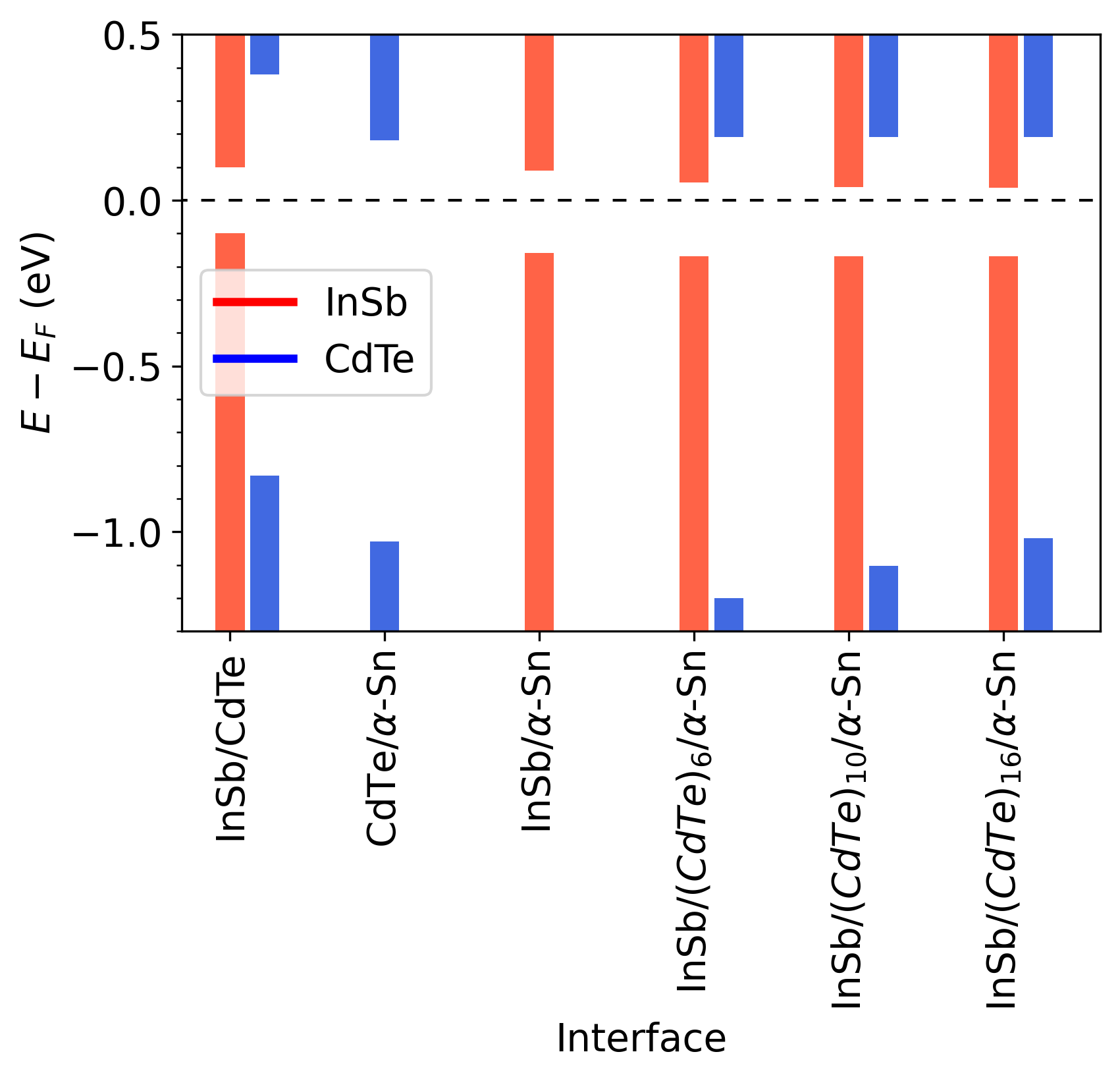
Figure 6 summarizes the band alignment at the bilayer and tri-layer interfaces studied here. For the tri-layer interfaces, the band alignment between the InSb and the -Sn is not significantly affected by the presence of CdTe, as shown in the element-projected band structures in the SI. The -Sn semi-metal point remains pinned at the Fermi level, as in the bilayer InSb/-Sn (see also Figure 4c). The InSb VBM remains at 0.17 eV below the Fermi level, similar to its position in the bilayer interface, regardless of the CdTe thickness. The InSb CBM position decreases slightly with the thickness of the CdTe from 0.09 eV above the Fermi level without CdTe, to 0.054 eV with 6 layers of CdTe, 0.04 eV with 10 layers, and 0.037 eV with 16 layers. This may be attributed to the quantum size effect, which causes a slight narrowing of the InSb gap because of the increase in the overall size of the system. Based on the element-projected band structures provided in the SI, the band edge positions of the CdTe are dominated by the interface with the -Sn, rather than the interface with the InSb. The CdTe CBM remains at 0.18 eV above the Fermi level, as in the bilayer CdTe/-Sn interface (see also Figure 4f), regardless of the number of layers. As the band gap of the CdTe narrows with increasing thickness, the CdTe VBM shifts from 1.24 eV below the Fermi level with 6 layers to 1.105 eV with 10 layers, and 1.05 eV with 16 layers, approaching the bilayer VBM position of 1.03 eV below the Fermi level with 42 layers. Although the band gap of the CdTe is significantly reduced due to MIGS, a type I band alignment with the InSb is maintained, similar to the bilayer InSb/CdTe interface (Figure 4g,i), as shown in Fig. 5 panels (a), (c), and (e).
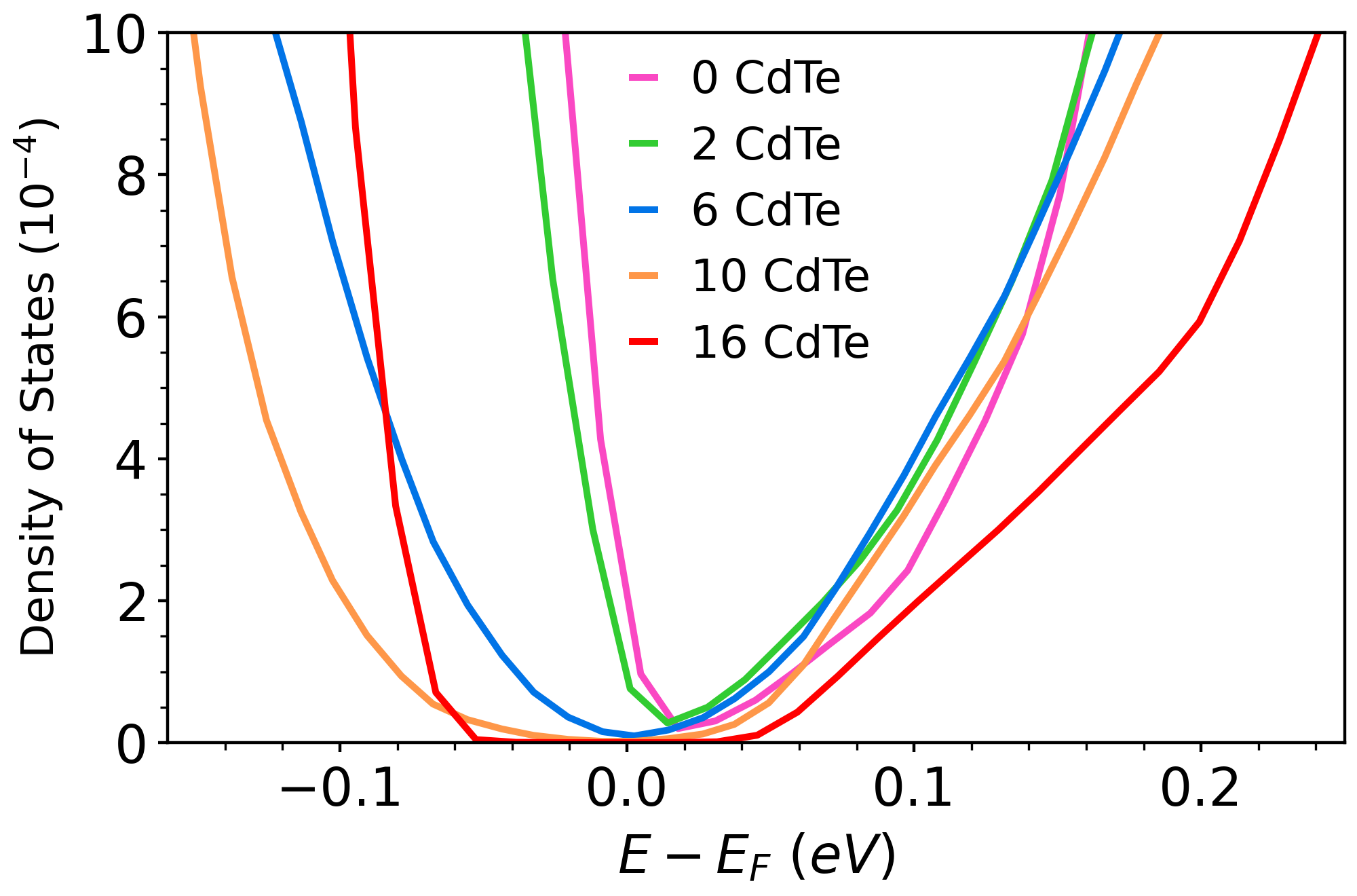
Figure 7 show the LDOS in the second layer of InSb from the interface as a function of the number of CdTe layers. Without CdTe and with two layers of CdTe, there is no band gap in the InSb close to the interface, owing to the significant density of MIGS. With 6 layers of CdTe the gap of the InSb close to the interface is still considerably narrower than its bulk value. The band gap in the second layer of InSb from the interface approaches its bulk value with 10 layers of CdTe and finally reaches it with 16 layers of CdTe. This suggests that 16 CdTe layers provide an effective barrier to electronically insulate the InSb from the -Sn. It is reasonable to assume that a barrier of this thickness or higher would all but eliminate transport through the interface into the InSb. Therefore, we estimate that the relevant barrier thickness regime to modulate the coupling at an interface with a superconductor and tune the proximity effect would be in the range of 6-10 layers, where MIGS still exist. We note, however, that the interface with -Sn may have somewhat different characteristics in terms of the band alignment and the penetration depth of MIGS.
IV Conclusion
In summary, we have used DFT with a Hubbard U correction machine-learned by Bayesian optimization to study CdTe as a prospective tunnel barrier at the InSb/-Sn interface. The results of PBE+U(BO) were validated by comparing the band structures of slab models of -Sn(001) and CdTe(111) with ARPES experiments (the PBE+U(BO) band structure of InSb(110) had been compared to ARPES experiments previously [63]). Excellent agreement with experiment is obtained for both materials. In particular, for the low-mean-free-path ARPES of CdTe, the z-unfolding scheme successfully reproduces the contributions of different values and modelling the 2 2 surface reconstruction successfully reproduces the contributions of surface states.
We then proceeded to use PBE+U(BO) to calculate the electronic structure of bilayer InSb/-Sn, CdTe/-Sn, and InSb/CdTe, as well as tri-layer InSb/CdTe/-Sn interfaces with varying thickness of CdTe. Simulations of these very large interface models were possible thanks to the balance between accuracy and computational cost provided by PBE+U(BO). We find that the most stable configuration of the InSb/CdTe interface is with In-Te and Sb-Cd bonding. MIGS penetrate from the -Sn into the InSn and CdTe. Similarly, states from the band edges of InSb penetrate into the larger gap of the CdTe. No interface states are found in any of the interfaces studied here, in contrast to the EuS/InAs interface, for example, in which a quantum well interface state emerges [110].
For all interfaces comprising -Sn, the semi-metal point is pinned at the Fermi level. For the tri-layer interface, the band alignment between the InSb and the -Sn remains the same as in the bilayer interface regardless of the thickness of the CdTe barrier, with the Fermi level closer to the conduction band edge of the InSb. The band edge positions of the CdTe are dominated by the interface with the -Sn rather than the interface with InSb, with the conduction band edge being closer to the Fermi level. A type-I band alignment is maintained between CdTe and InSb with the gap of the former straddling the latter. The CBM of the CdTe is pinned whereas the VBM shifts upwards towards the Fermi level as the gap narrows with the increase in thickness.
We find that 16 layers of CdTe (about 3.5 nm) serve as an effective barrier, preventing the penetration of MIGS from the -Sn into the InSb. However, in the context of Majorana experiments, it is possible that a barrier thick enough to completely insulate the semiconductor from the superconductor would also all but eliminate transport. Therefore, we estimate that the relevant regime for tuning the coupling at the interface would be in the thickness range where some MIGS are still present, while thicker CdTe layers could be used to passivate exposed InSb surfaces. We note, however, that the interface with the superconducting -Sn, which is not lattice matched to InSb and CdTe, may have different characteristics than the interface with -Sn. In practice, careful experimentation with varying barrier thickness would be needed to determine the optimal configuration for MZM devices.
We have thus demonstrated that DFT simulations can provide useful insight into the electronic properties of semiconductor/tunnel barrier/metal interfaces. This includes the interface bonding configuration, the band alignment, and the presence of MIGS (and, possibly, of interface states). Such simulations may be conducted for additional interfaces to explore other prospective material combinations. This may inform the choice of interface systems and the design of future Majorana experiments. More broadly, similar DFT simulations of interfaces may be performed to evaluate prospective tunnel barriers e.g., for semiconductor devices.
V Acknowledgements
We thank Guang Bian from the University of Missouri, Li Fu from Northwestern Polytechnical University, China, and Tai C. Chiang from the University of Illinois at Urbana-Champaign for sharing their ARPES data for CdTe. Work at the University of Pittsburgh was supported by the Department of Energy through grant DE-SC-0019274. Work at CMU and UCSB was funded by the National Science Foundation (NSF) through grant OISE-1743717. Work in Grenoble is supported by the ANR-NSF PIRE:HYBRID, Transatlantic Research Partnership and IRP-CNRS HYNATOQ. This research used computing resources of the University of Pittsburgh Center for Research Computing, which is supported by NIH award number S10OD028483 and of the National Energy Research Scientific Computing Center (NERSC), a U.S. Department of Energy Office of Science User Facility operated under Contract No. DE-AC02-05CH11231.
References
- Aasen et al. [2016] D. Aasen, M. Hell, R. V. Mishmash, A. Higginbotham, J. Danon, M. Leijnse, T. S. Jespersen, J. A. Folk, C. M. Marcus, K. Flensberg, and J. Alicea, Milestones toward majorana-based quantum computing, Phys. Rev. X 6, 031016 (2016).
- Sarma et al. [2015] S. D. Sarma, M. Freedman, and C. Nayak, Majorana zero modes and topological quantum computation, npj Quantum Information 1, 15001 (2015).
- Oreg et al. [2010] Y. Oreg, G. Refael, and F. von Oppen, Helical liquids and majorana bound states in quantum wires, Phys. Rev. Lett. 105, 177002 (2010).
- Lutchyn et al. [2010] R. M. Lutchyn, J. D. Sau, and S. Das Sarma, Majorana fermions and a topological phase transition in semiconductor-superconductor heterostructures, Phys. Rev. Lett. 105, 077001 (2010).
- Mourik et al. [2012] V. Mourik, K. Zuo, S. M. Frolov, S. R. Plissard, E. P. A. M. Bakkers, and L. P. Kouwenhoven, Signatures of majorana fermions in hybrid superconductor-semiconductor nanowire devices, Science 336, 1003 (2012).
- Leijnse and Flensberg [2012] M. Leijnse and K. Flensberg, Introduction to topological superconductivity and majorana fermions, Semiconductor Science and Technology 27, 124003 (2012).
- Fu et al. [2021] J.-B. Fu, B. Li, X.-F. Zhang, G.-Z. Yu, G.-Y. Huang, and M.-T. Deng, Experimental review on majorana zero-modes in hybrid nanowires, Science China Physics, Mechanics & Astronomy 64, 107001 (2021).
- Yu et al. [2021a] P. Yu, J. Chen, M. Gomanko, G. Badawy, E. P. A. M. Bakkers, K. Zuo, V. Mourik, and S. M. Frolov, Non-majorana states yield nearly quantized conductance in proximatized nanowires, Nature Physics 17, 482 (2021a).
- Kells et al. [2012] G. Kells, D. Meidan, and P. W. Brouwer, Near-zero-energy end states in topologically trivial spin-orbit coupled superconducting nanowires with a smooth confinement, Phys. Rev. B 86, 100503 (2012).
- Frolov et al. [2020] S. M. Frolov, M. J. Manfra, and J. D. Sau, Topological superconductivity in hybrid devices, Nature Physics 16, 718 (2020).
- Khan et al. [2020] S. A. Khan, C. Lampadaris, A. Cui, L. Stampfer, Y. Liu, S. J. Pauka, M. E. Cachaza, E. M. Fiordaliso, J.-H. Kang, S. Korneychuk, T. Mutas, J. E. Sestoft, F. Krizek, R. Tanta, M. C. Cassidy, T. S. Jespersen, and P. Krogstrup, Highly transparent gatable superconducting shadow junctions, ACS Nano 14, 14605 (2020).
- Pendharkar et al. [2021] M. Pendharkar, B. Zhang, H. Wu, A. Zarassi, P. Zhang, C. P. Dempsey, J. S. Lee, S. D. Harrington, G. Badawy, S. Gazibegovic, R. L. M. O. het Veld, M. Rossi, J. Jung, A.-H. Chen, M. A. Verheijen, M. Hocevar, E. P. A. M. Bakkers, C. J. Palmstrøm, and S. M. Frolov, Parity-preserving and magnetic field-resilient superconductivity in InSb nanowires with Sn shells, Science 372, 508 (2021).
- Krogstrup et al. [2015] P. Krogstrup, N. L. B. Ziino, W. Chang, S. M. Albrecht, M. H. Madsen, E. Johnson, J. Nygård, C. M. Marcus, and T. S. Jespersen, Epitaxy of semiconductor–superconductor nanowires, Nature Materials 14, 400 (2015).
- Op het Veld et al. [2020] R. L. M. Op het Veld, D. Xu, V. Schaller, M. A. Verheijen, S. M. E. Peters, J. Jung, C. Tong, Q. Wang, M. W. A. de Moor, B. Hesselmann, K. Vermeulen, J. D. S. Bommer, J. Sue Lee, A. Sarikov, M. Pendharkar, A. Marzegalli, S. Koelling, L. P. Kouwenhoven, L. Miglio, C. J. Palmstrøm, H. Zhang, and E. P. A. M. Bakkers, In-plane selective area InSb-Al nanowire quantum networks, Communications Physics 3, 59 (2020).
- Carrad et al. [2020] D. J. Carrad, M. Bjergfelt, T. Kanne, M. Aagesen, F. Krizek, E. M. Fiordaliso, E. Johnson, J. Nygård, and T. S. Jespersen, Shadow epitaxy for in situ growth of generic semiconductor/superconductor hybrids, Advanced Materials 32, 1908411 (2020).
- Kanne et al. [2021] T. Kanne, M. Marnauza, D. Olsteins, D. J. Carrad, J. E. Sestoft, J. de Bruijckere, L. Zeng, E. Johnson, E. Olsson, K. Grove-Rasmussen, and J. Nygård, Epitaxial pb on inas nanowires for quantum devices, Nature Nanotechnology 16, 776 (2021).
- Harper et al. [2019] F. Harper, A. Pushp, and R. Roy, Majorana braiding in realistic nanowire y-junctions and tuning forks, Phys. Rev. Research 1, 033207 (2019).
- Jardine et al. [2021] M. J. A. Jardine, J. P. T. Stenger, Y. Jiang, E. J. de Jong, W. Wang, A. C. B. Jayich, and S. M. Frolov, Integrating micromagnets and hybrid nanowires for topological quantum computing, SciPost Phys. 11, 90 (2021).
- Reeg et al. [2018] C. Reeg, D. Loss, and J. Klinovaja, Metallization of a rashba wire by a superconducting layer in the strong-proximity regime, Phys. Rev. B 97, 165425 (2018).
- Antipov et al. [2018] A. E. Antipov, A. Bargerbos, G. W. Winkler, B. Bauer, E. Rossi, and R. M. Lutchyn, Effects of gate-induced electric fields on semiconductor majorana nanowires, Phys. Rev. X 8, 031041 (2018).
- Vail et al. [2021] O. Vail, A. Chang, S. Harrington, P. Folkes, P. Taylor, B. Nichols, C. Palmstrøm, and G. de Coster, Gated magnetotransport in -Sn thin films on CdTe, Journal of Electronic Materials 50, 6329 (2021).
- Reeg et al. [2017] C. Reeg, D. Loss, and J. Klinovaja, Finite-size effects in a nanowire strongly coupled to a thin superconducting shell, Phys. Rev. B 96, 125426 (2017).
- Badawy et al. [2019] G. Badawy, S. Gazibegovic, F. Borsoi, S. Heedt, C.-A. Wang, S. Koelling, M. A. Verheijen, L. P. Kouwenhoven, and E. P. A. M. Bakkers, High mobility stemless InSb nanowires, Nano Letters, Nano Letters 19, 3575 (2019).
- Cole et al. [2015] W. S. Cole, S. Das Sarma, and T. D. Stanescu, Effects of large induced superconducting gap on semiconductor majorana nanowires, Phys. Rev. B 92, 174511 (2015).
- Badawy et al. [2022] G. Badawy, B. Zhang, T. Rauch, J. Momand, S. Koelling, J. Jung, S. Gazibegovic, O. Moutanabbir, B. J. Kooi, S. Botti, M. A. Verheijen, S. M. Frolov, and E. P. A. M. Bakkers, Electronic structure and epitaxy of CdTe shells on InSb nanowires, Advanced Science 9, 2105722 (2022).
- Suarez Negreira et al. [2015] A. Suarez Negreira, W. G. Vandenberghe, and M. V. Fischetti, Ab initio study of the electronic properties and thermodynamic stability of supported and functionalized two-dimensional Sn films, Phys. Rev. B 91, 245103 (2015).
- Rogalev et al. [2017] V. A. Rogalev, T. c. v. Rauch, M. R. Scholz, F. Reis, L. Dudy, A. Fleszar, M.-A. Husanu, V. N. Strocov, J. Henk, I. Mertig, J. Schäfer, and R. Claessen, Double band inversion in -Sn: Appearance of topological surface states and the role of orbital composition, Phys. Rev. B 95, 161117 (2017).
- Chen et al. [2022] K. H. M. Chen, K. Y. Lin, S. W. Lien, S. W. Huang, C. K. Cheng, H. Y. Lin, C.-H. Hsu, T.-R. Chang, C.-M. Cheng, M. Hong, and J. Kwo, Thickness-dependent topological phase transition and rashba-like preformed topological surface states of -Sn(001) thin films on InSb(001), Phys. Rev. B 105, 075109 (2022).
- Shi et al. [2020] Z. Shi, X. Wang, C. Xu, P. Wang, Y. Liu, and T.-C. Chiang, First-principles study of the topological surface states of-Sn(111), Physics Letters A 384, 126782 (2020).
- Xu et al. [2017] C.-Z. Xu, Y.-H. Chan, Y. Chen, P. Chen, X. Wang, C. Dejoie, M.-H. Wong, J. A. Hlevyack, H. Ryu, H.-Y. Kee, N. Tamura, M.-Y. Chou, Z. Hussain, S.-K. Mo, and T.-C. Chiang, Elemental topological dirac semimetal: -Sn on InSb(111), Phys. Rev. Lett. 118, 146402 (2017).
- Huang and Liu [2017] H. Huang and F. Liu, Tensile strained gray tin: Dirac semimetal for observing negative magnetoresistance with shubnikov–de haas oscillations, Phys. Rev. B 95, 201101 (2017).
- Vail et al. [2020] O. Vail, P. Taylor, P. Folkes, B. Nichols, B. Haidet, K. Mukherjee, and G. de Coster, Growth and magnetotransport in thin-film -Sn on CdTe, physica status solidi (b) 257, 1800513 (2020).
- de Coster et al. [2018] G. J. de Coster, P. A. Folkes, P. J. Taylor, and O. A. Vail, Effects of orientation and strain on the topological characteristics of CdTe/-Sn quantum wells, Phys. Rev. B 98, 115153 (2018).
- Madarevic et al. [2020] I. Madarevic, U. Thupakula, G. Lippertz, N. Claessens, P.-C. Lin, H. Bana, S. Gonzalez, G. Di Santo, L. Petaccia, M. N. Nair, L. M. Pereira, C. Van Haesendonck, and M. J. Van Bael, Structural and electronic properties of the pure and stable elemental 3d topological dirac semimetal -Sn, APL Materials 8, 031114 (2020).
- Barfuss et al. [2013] A. Barfuss, L. Dudy, M. R. Scholz, H. Roth, P. Höpfner, C. Blumenstein, G. Landolt, J. H. Dil, N. C. Plumb, M. Radovic, A. Bostwick, E. Rotenberg, A. Fleszar, G. Bihlmayer, D. Wortmann, G. Li, W. Hanke, R. Claessen, and J. Schäfer, Elemental topological insulator with tunable fermi level: Strained -sn on InSb(001), Phys. Rev. Lett. 111, 157205 (2013).
- Scholz et al. [2018] M. R. Scholz, V. A. Rogalev, L. Dudy, F. Reis, F. Adler, J. Aulbach, L. J. Collins-McIntyre, L. B. Duffy, H. F. Yang, Y. L. Chen, T. Hesjedal, Z. K. Liu, M. Hoesch, S. Muff, J. H. Dil, J. Schäfer, and R. Claessen, Topological surface state of Sn on InSb(001) as studied by photoemission, Phys. Rev. B 97, 075101 (2018).
- Ohtsubo et al. [2013] Y. Ohtsubo, P. Le Fèvre, F. m. c. Bertran, and A. Taleb-Ibrahimi, Dirac cone with helical spin polarization in ultrathin -Sn(001) films, Phys. Rev. Lett. 111, 216401 (2013).
- Fu and Kane [2007] L. Fu and C. L. Kane, Topological insulators with inversion symmetry, Phys. Rev. B 76, 045302 (2007).
- Khan et al. [2022] S. A. Khan, S. Martí-Sánchez, D. Olsteins, C. Lampadaris, D. J. Carrad, Y. Liu, J. Quiñones, M. C. Spadaro, T. S. Jespersen, P. Krogstrup, and J. Arbiol, Epitaxially driven phase selectivity of sn in hybrid quantum nanowires, arXiv , 2212.13314 (2022).
- Farrow et al. [1981] R. F. C. Farrow, D. S. Robertson, G. M. Williams, A. G. Cullis, G. R. Jones, I. M. Young, and P. N. J. Dennis, The growth of metastable, heteroepitaxial films of -Sn by metal beam epitaxy, Journal of Crystal Growth 54, 507 (1981).
- Song et al. [2019] H. Song, J. Yao, Y. Ding, Y. Gu, Y. Deng, M.-H. Lu, H. Lu, and Y.-F. Chen, Thermal stability enhancement in epitaxial alpha tin films by strain engineering, Advanced Engineering Materials 21, 1900410 (2019).
- Davydov et al. [2020] A. Davydov, A. Sanna, C. Pellegrini, J. K. Dewhurst, S. Sharma, and E. K. U. Gross, Ab initio theory of plasmonic superconductivity within the eliashberg and density-functional formalisms, Phys. Rev. B 102, 214508 (2020).
- Sanna et al. [2020] A. Sanna, C. Pellegrini, and E. K. U. Gross, Combining eliashberg theory with density functional theory for the accurate prediction of superconducting transition temperatures and gap functions, Phys. Rev. Lett. 125, 057001 (2020).
- Winkler et al. [2019] G. W. Winkler, A. E. Antipov, B. van Heck, A. A. Soluyanov, L. I. Glazman, M. Wimmer, and R. M. Lutchyn, Unified numerical approach to topological semiconductor-superconductor heterostructures, Phys. Rev. B 99, 245408 (2019).
- Schuwalow et al. [2021] S. Schuwalow, N. B. M. Schröter, J. Gukelberger, C. Thomas, V. Strocov, J. Gamble, A. Chikina, M. Caputo, J. Krieger, G. C. Gardner, M. Troyer, G. Aeppli, M. J. Manfra, and P. Krogstrup, Band structure extraction at hybrid narrow-gap semiconductor-metal interfaces, Advanced Science 8, 2003087 (2021).
- Borlido et al. [2019] P. Borlido, T. Aull, A. W. Huran, F. Tran, M. A. L. Marques, and S. Botti, Large-scale benchmark of exchange-correlation functionals for the determination of electronic band gaps of solids, Journal of Chemical Theory and Computation 15, 5069 (2019).
- Bennett et al. [2019] J. W. Bennett, B. G. Hudson, I. K. Metz, D. Liang, S. Spurgeon, Q. Cui, and S. E. Mason, A systematic determination of hubbard u using the gbrv ultrasoft pseudopotential set, Computational Materials Science 170, 109137 (2019).
- Huang et al. [2016] X. Huang, S. K. Ramadugu, and S. E. Mason, Surface-specific DFT + U approach applied to -, The Journal of Physical Chemistry C 120, 4919 (2016).
- Peverati and Truhlar [2012] R. Peverati and D. G. Truhlar, Performance of the m11-l density functional for bandgaps and lattice constants of unary and binary semiconductors, The Journal of Chemical Physics 136, 134704 (2012).
- Perdew et al. [1981] J. P. Perdew, E. R. McMullen, and A. Zunger, Density-functional theory of the correlation energy in atoms and ions: A simple analytic model and a challenge, Phys. Rev. A 23, 2785 (1981).
- Mori-Sánchez et al. [2006] P. Mori-Sánchez, A. J. Cohen, and W. Yang, Many-electron self-interaction error in approximate density functionals, The Journal of Chemical Physics 125, 201102 (2006).
- Mori-Sánchez et al. [2008] P. Mori-Sánchez, A. J. Cohen, and W. Yang, Localization and delocalization errors in density functional theory and implications for band-gap prediction, Phys. Rev. Lett. 100, 146401 (2008).
- Zhang et al. [2018] G.-X. Zhang, A. M. Reilly, A. Tkatchenko, and M. Scheffler, Performance of various density-functional approximations for cohesive properties of 64 bulk solids, New Journal of Physics 20, 063020 (2018).
- Garza and Scuseria [2016] A. J. Garza and G. E. Scuseria, Predicting band gaps with hybrid density functionals, The Journal of Physical Chemistry Letters 7, 4165 (2016).
- Yu et al. [2020] M. Yu, S. Yang, C. Wu, and N. Marom, Machine learning the hubbard u parameter in dft+u using bayesian optimization, npj Computational Materials 6, 180 (2020).
- Yang et al. [2021] S. Yang, D. Dardzinski, A. Hwang, D. I. Pikulin, G. W. Winkler, and N. Marom, First-principles feasibility assessment of a topological insulator at the inas/gasb interface, Phys. Rev. Materials 5, 084204 (2021).
- Rohlfing et al. [1998] M. Rohlfing, P. Krüger, and J. Pollmann, Role of semicore electrons in quasiparticle band-structure calculations, Phys. Rev. B 57, 6485 (1998).
- Küfner et al. [2013] S. Küfner, J. Furthmüller, L. Matthes, M. Fitzner, and F. Bechstedt, Structural and electronic properties of -tin nanocrystals from first principles, Phys. Rev. B 87, 235307 (2013).
- Dardzinski et al. [2022] D. Dardzinski, M. Yu, S. Moayedpour, and N. Marom, Best practices for first-principles simulations of epitaxial inorganic interfaces, Journal of Physics: Condensed Matter (2022).
- Xu et al. [2018] C.-Z. Xu, Y.-H. Chan, P. Chen, X. Wang, D. Flötotto, J. A. Hlevyack, G. Bian, S.-K. Mo, M.-Y. Chou, and T.-C. Chiang, Gapped electronic structure of epitaxial stanene on InSb(111), Phys. Rev. B 97, 035122 (2018).
- Küfner et al. [2014] S. Küfner, M. Fitzner, and F. Bechstedt, Topological -Sn surface states versus film thickness and strain, Phys. Rev. B 90, 125312 (2014).
- Rogalev et al. [2019] V. A. Rogalev, F. Reis, F. Adler, M. Bauernfeind, J. Erhardt, A. Kowalewski, M. R. Scholz, L. Dudy, L. B. Duffy, T. Hesjedal, M. Hoesch, G. Bihlmayer, J. Schäfer, and R. Claessen, Tailoring the topological surface state in ultrathin -Sn(111) films, Phys. Rev. B 100, 245144 (2019).
- Yang et al. [2022] S. Yang, N. B. M. Schröter, V. N. Strocov, S. Schuwalow, M. Rajpalk, K. Ohtani, P. Krogstrup, G. W. Winkler, J. Gukelberger, D. Gresch, G. Aeppli, R. M. Lutchyn, and N. Marom, Electronic structure of InAs and InSb surfaces: Density functional theory and angle-resolved photoemission spectroscopy, Advanced Quantum Technologies 5, 2100033 (2022).
- Popescu and Zunger [2012] V. Popescu and A. Zunger, Extracting versus effective band structure from supercell calculations on alloys and impurities, Phys. Rev. B 85, 085201 (2012).
- Ku et al. [2010] W. Ku, T. Berlijn, and C.-C. Lee, Unfolding first-principles band structures, Phys. Rev. Lett. 104, 216401 (2010).
- Herath et al. [2020] U. Herath, P. Tavadze, X. He, E. Bousquet, S. Singh, F. Muñoz, and A. H. Romero, Pyprocar: A python library for electronic structure pre/post-processing, Computer Physics Communications 251, 107080 (2020).
- Wang et al. [2021] V. Wang, N. Xu, J.-C. Liu, G. Tang, and W.-T. Geng, Vaspkit: A user-friendly interface facilitating high-throughput computing and analysis using vasp code, Computer Physics Communications 267, 108033 (2021).
- Medeiros et al. [2014] P. V. C. Medeiros, S. Stafström, and J. Björk, Effects of extrinsic and intrinsic perturbations on the electronic structure of graphene: Retaining an effective primitive cell band structure by band unfolding, Phys. Rev. B 89, 041407 (2014).
- Iwasawa [2020] H. Iwasawa, High-resolution angle-resolved photoemission spectroscopy and microscopy, Electronic Structure 2, 043001 (2020).
- Seah and Dench [1979] M. P. Seah and W. A. Dench, Quantitative electron spectroscopy of surfaces: A standard data base for electron inelastic mean free paths in solids, Surface and Interface Analysis 1, 2 (1979).
- Zhang et al. [2022] H. Zhang, T. Pincelli, C. Jozwiak, T. Kondo, R. Ernstorfer, T. Sato, and S. Zhou, Angle-resolved photoemission spectroscopy, Nature Reviews Methods Primers 2, 54 (2022).
- Kumigashira et al. [1998] H. Kumigashira, H.-D. Kim, T. Ito, A. Ashihara, T. Takahashi, T. Suzuki, M. Nishimura, O. Sakai, Y. Kaneta, and H. Harima, High-resolution angle-resolved photoemission study of lasb, Phys. Rev. B 58, 7675 (1998).
- Feibelman and Eastman [1974] P. J. Feibelman and D. E. Eastman, Photoemission spectroscopy—correspondence between quantum theory and experimental phenomenology, Phys. Rev. B 10, 4932 (1974).
- Strocov [2003] V. Strocov, Intrinsic accuracy in 3-dimensional photoemission band mapping, Journal of Electron Spectroscopy and Related Phenomena 130, 65 (2003).
- Strocov et al. [2012] V. N. Strocov, M. Shi, M. Kobayashi, C. Monney, X. Wang, J. Krempasky, T. Schmitt, L. Patthey, H. Berger, and P. Blaha, Three-dimensional electron realm in by soft-x-ray photoelectron spectroscopy: Origin of charge-density waves, Phys. Rev. Lett. 109, 086401 (2012).
- Strocov et al. [1997] V. N. Strocov, H. I. Starnberg, and P. O. Nilsson, Excited-state bands of cu determined by vleed band fitting and their implications for photoemission, Phys. Rev. B 56, 1717 (1997).
- Strocov et al. [2023] V. N. Strocov, L. L. Lev, F. Alarab, P. Constantinou, T. Schmitt, T. J. Z. Stock, L. Nicolaï, J. Očenášek, and J. Minár, Are high-energy photoemission final states free-electron-like?, arXiv , 2301.00033 (2023).
- Strocov et al. [2006] V. N. Strocov, E. E. Krasovskii, W. Schattke, N. Barrett, H. Berger, D. Schrupp, and R. Claessen, Three-dimensional band structure of layered : Photoemission final-state effects, Phys. Rev. B 74, 195125 (2006).
- Krasovskii et al. [2007] E. E. Krasovskii, V. N. Strocov, N. Barrett, H. Berger, W. Schattke, and R. Claessen, Band mapping in the one-step photoemission theory: Multi-bloch-wave structure of final states and interference effects, Phys. Rev. B 75, 045432 (2007).
- Kresse and Hafner [1993] G. Kresse and J. Hafner, Ab initio molecular dynamics for liquid metals, Phys. Rev. B 47, 558 (1993).
- Blöchl [1994] P. E. Blöchl, Projector augmented-wave method, Phys. Rev. B 50, 17953 (1994).
- Kresse and Joubert [1999] G. Kresse and D. Joubert, From ultrasoft pseudopotentials to the projector augmented-wave method, Phys. Rev. B 59, 1758 (1999).
- Perdew et al. [1996] J. P. Perdew, K. Burke, and M. Ernzerhof, Generalized gradient approximation made simple, Phys. Rev. Lett. 77, 3865 (1996).
- Dudarev et al. [1998] S. L. Dudarev, G. A. Botton, S. Y. Savrasov, C. J. Humphreys, and A. P. Sutton, Electron-energy-loss spectra and the structural stability of nickel oxide: An lsda+u study, Phys. Rev. B 57, 1505 (1998).
- Heyd et al. [2003] J. Heyd, G. E. Scuseria, and M. Ernzerhof, Hybrid functionals based on a screened coulomb potential, The Journal of Chemical Physics 118, 8207 (2003).
- Wu et al. [2015] Y. Wu, G. Chen, Y. Zhu, W.-J. Yin, Y. Yan, M. Al-Jassim, and S. J. Pennycook, LDA+U/GGA+U calculations of structural and electronic properties of CdTe: Dependence on the effective u parameter, Computational Materials Science 98, 18 (2015).
- Fonthal et al. [2000] G. Fonthal, L. Tirado-Mejía, J. Marín-Hurtado, H. Ariza-Calderón, and J. Menddoza-Alvarez, Temperature dependence of the band gap energy of crystalline CdTe, Journal of Physics and Chemistry of Solids 61, 579 (2000).
- Hinuma et al. [2014] Y. Hinuma, A. Grüneis, G. Kresse, and F. Oba, Band alignment of semiconductors from density-functional theory and many-body perturbation theory, Phys. Rev. B 90, 155405 (2014).
- Neugebauer and Scheffler [1992] J. Neugebauer and M. Scheffler, Adsorbate-substrate and adsorbate-adsorbate interactions of na and k adlayers on al(111), Phys. Rev. B 46, 16067 (1992).
- Vurgaftman et al. [2001] I. Vurgaftman, J. R. Meyer, and L. R. Ram-Mohan, Band parameters for III-V compound semiconductors and their alloys, Journal of Applied Physics 89, 5815 (2001).
- Huang et al. [2005] X. Huang, E. Lindgren, and J. R. Chelikowsky, Surface passivation method for semiconductor nanostructures, Phys. Rev. B 71, 165328 (2005).
- Yang et al. [2020] S. Yang, C. Wu, and N. Marom, Topological properties of snse/eus and snte/cate interfaces, Phys. Rev. Materials 4, 034203 (2020).
- Ren et al. [2015] J. Ren, L. Fu, G. Bian, M. Wong, T. Wang, G. Zha, W. Jie, T. Miller, M. Z. Hasan, and T.-C. Chiang, Spectroscopic studies of CdTe bulk and surface electronic structure, Phys. Rev. B 91, 235303 (2015).
- Kronik and Kümmel [2014] L. Kronik and S. Kümmel, Gas-phase valence-electron photoemission spectroscopy using density functional theory, in First Principles Approaches to Spectroscopic Properties of Complex Materials, edited by C. Di Valentin, S. Botti, and M. Cococcioni (Springer Berlin Heidelberg, Berlin, Heidelberg, 2014) pp. 137–191.
- Krukau et al. [2006] A. V. Krukau, O. A. Vydrov, A. F. Izmaylov, and G. E. Scuseria, Influence of the exchange screening parameter on the performance of screened hybrid functionals, The Journal of Chemical Physics 125, 224106 (2006).
- Egan et al. [2011] C. K. Egan, Q. Z. Jiang, and A. W. Brinkman, Morphology and reconstructions of polar CdTe(111)a,b surfaces by scanning tunneling microscopy, Journal of Vacuum Science & Technology A 29, 011021 (2011).
- Tersoff [1986] J. Tersoff, Calculation of Schottky barrier heights from semiconductor band structures, Surface Science 168, 275 (1986).
- Mönch [1996] W. Mönch, Empirical tight‐binding calculation of the branch‐point energy of the continuum of interface‐induced gap states, Journal of Applied Physics 80, 5076 (1996).
- Mönch [1987] W. Mönch, Role of virtual gap states and defects in metal-semiconductor contacts, Phys. Rev. Lett. 58, 1260 (1987).
- Mönch [1999] W. Mönch, Barrier heights of real schottky contacts explained by metal-induced gap states and lateral inhomogeneities, Journal of Vacuum Science & Technology B: Microelectronics and Nanometer Structures Processing, Measurement, and Phenomena 17, 1867 (1999).
- Monch [1990] W. Monch, On the physics of metal-semiconductor interfaces, Reports on Progress in Physics 53, 221 (1990).
- Robertson [2013] J. Robertson, Band offsets, schottky barrier heights, and their effects on electronic devices, Journal of Vacuum Science & Technology A 31, 050821 (2013).
- Tang et al. [1987] M. Tang, D. W. Niles, I. Hernández-Calderón, and H. Höchst, Angle-resolved photoemission study of the -Sn/CdTe(100) interface, Phys. Rev. B 36, 3336 (1987).
- Takatani and Chung [1985] S. Takatani and Y. W. Chung, Thin-film quantization studies of grey tin epitaxially grown on CdTe(111), Phys. Rev. B 31, 2290 (1985).
- Höchst et al. [1988] H. Höchst, D. W. Niles, and I. Hernández‐Calderón, Interface and growth studies of -Sn/CdTe(110) superlattices, Journal of Vacuum Science & Technology B: Microelectronics Processing and Phenomena 6, 1219 (1988).
- Lambrecht and Segall [1990] W. R. L. Lambrecht and B. Segall, Interface-bond-polarity model for semiconductor heterojunction band offsets, Phys. Rev. B 41, 2832 (1990).
- Continenza and Freeman [1992] A. Continenza and A. J. Freeman, Band lineup and electric fields in (-sn/(cdte [001] and [110] superlattices, Phys. Rev. B 45, 5953 (1992).
- Cardona and Christensen [1987] M. Cardona and N. E. Christensen, Acoustic deformation potentials and heterostructure band offsets in semiconductors, Phys. Rev. B 35, 6182 (1987).
- Wang et al. [2018] X. Wang, C. Campbell, Y.-H. Zhang, and R. J. Nemanich, Band alignment at the CdTe/InSb (001) heterointerface, Journal of Vacuum Science & Technology A 36, 031101 (2018).
- Yu et al. [2021b] M. Yu, S. Moayedpour, S. Yang, D. Dardzinski, C. Wu, V. S. Pribiag, and N. Marom, Dependence of the electronic structure of the eus/inas interface on the bonding configuration, Phys. Rev. Mater. 5, 064606 (2021b).