Berry curvature induced valley Hall effect in non-encapsulated hBN/Bilayer graphene heterostructure aligned with near-zero twist angle
Abstract
Valley Hall effect has been observed in asymmetric single-layer and bilayer graphene systems. In single-layer graphene systems, asymmetry is introduced by aligning graphene with hexagonal boron nitride (hBN) with a near-zero twist angle, breaking the sub-lattice symmetry. Although a similar approach has been used in bilayer graphene to break the layer symmetry and thereby observe the valley Hall effect, the bilayer graphene was sandwiched with hBN on both sides in those studies. This study looks at a much simpler, non-encapsulated structure where hBN is present only at the top of graphene. The crystallographic axes of both hBN and bilayer graphene are aligned. A clear signature of the valley Hall effect through non-local resistance measurement () was observed. The observed non-local resistance could be manipulated by applying a displacement field across the heterostructure. Furthermore, the electronic band structure and Berry curvature calculations validate the experimental observations.
With the introduction of two-dimensional materials, the valley degree of freedom of carriers has gained much prominence in recent years Schaibley-2016 ; Vitale-2018 ; Xu-2014 . Materials like graphene and MoS2 have two in-equivalent valleys at the K and K′ high symmetry points of their Brillouin zone, which can be interpreted as valley-up and valley-down, much like the spin degree of freedom of carriers. However, the fundamental criterion for a material to be valleytronic is to have a broken inversion symmetry. While single-layer graphene is symmetric, aligning graphene with hexagonal boron nitride (hBN) with a near-zero twist angle has proved to break the sub-lattice symmetry of the graphene layer Yankowitz-2012 ; Woods-2014 ; Song-2015 ; Yankowitz-2019 . Such a system has exhibited the valley Hall effect (VHE) due to the emergence of Berry curvature at the valley as a result of broken inversion symmetry Gorbachev-2014 ; Komatsu-2018 ; Li-2020 . As for bilayer graphene, the asymmetry can be introduced by either applying an out-of-plane electric field across the layers or by aligning with an hBN layer, both of which break the layer symmetry of the system as they introduce different potentials between the top and bottom layers of the bilayer McCann-2006 ; Min-2007 ; Oostinga-2007 ; Zhang-2009 ; Dean-2013 . Both methods have been employed to observe VHE in bilayer graphene in recent years Sui-2015 ; Shimazaki-2015 ; Endo-2019 ; Arrighi-2022 .
In the case of single-layer graphene, it has been shown that both encapsulated and non-encapsulated graphene exhibit the valley Hall effect, provided either of the hBN (top or bottom) is oriented with graphene Gorbachev-2014 . As for bilayer graphene, the valley Hall effect is observed by hBN alignment only in encapsulated systems Endo-2019 ; Arrighi-2022 . Here hBN is present at the top and bottom of the bilayer graphene with one of the hBN aligned and the other misaligned by more than 10∘ to avoid the formation of a double moire pattern. However, it has been shown theoretically that aligning hBN with bilayer graphene in a non-encapsulated configuration can also break the symmetry of the system and induce Berry curvature Afsal-2020 . Considering the difficulty in fabricating encapsulated bilayer graphene heterostructure, in this study, we explore the VHE in non-encapsulated hBN/bilayer graphene heterostructure (hBN/bilayer graphene/SiO2) with the hBN aligned with the bilayer graphene. We observed a strong VHE signal at the primary Dirac point through non-local electrical measurement. The VHE signal could be further manipulated by applying a displacement electric field across the layers. We also performed ab initio calculations, which show that aligned hBN/bilayer graphene heterostructure has an intrinsic band gap and a non-zero Berry curvature. The band gap and the Berry curvature can be manipulated with an out-of-plane electric field applied across the layers.
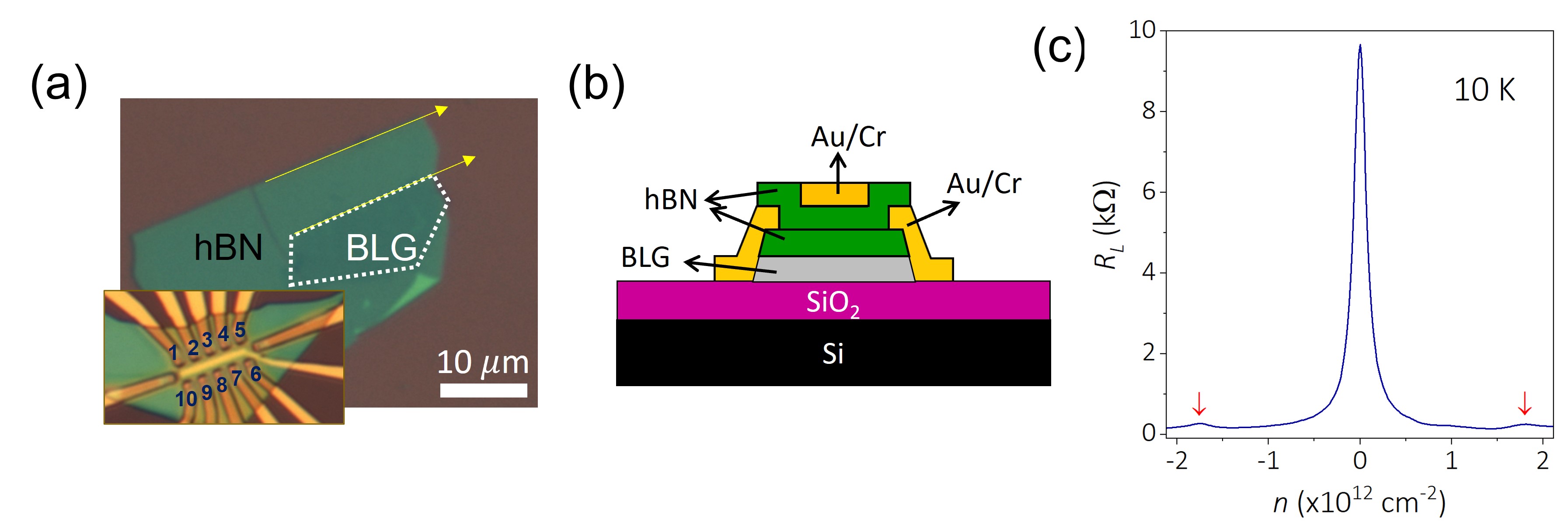
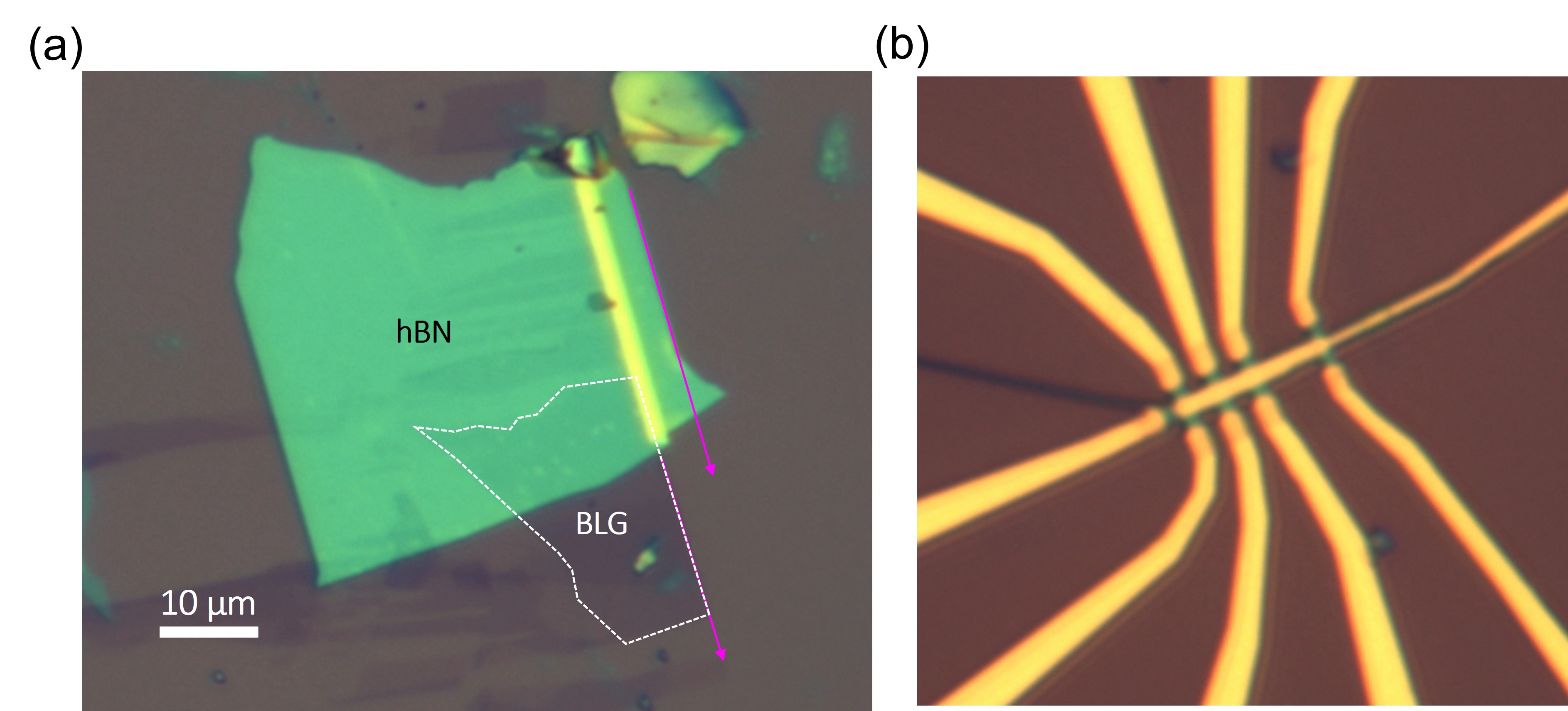
The hBN/bilayer graphene heterostructure is fabricated following the dry transfer method Wang-2013 . Two devices denoted as Device A and Device B, are fabricated. The results presented in the main text are from Device A (see supplementary information for the results from Device B). Figure 1a shows the optical image of the hBN/bilayer graphene heterostructure from which Device A is fabricated. The dotted line outlines the bilayer graphene area. The arrows indicate the edges of hBN and bilayer graphene, which are aligned with a near-zero twist angle. After etching the heterostructure into a Hall bar, edge contacts were fabricated Wang-2013 . Later a passivation hBN layer is transferred on top of the heterostructure, above which the top gate electrode is fabricated. Figure 1a inset and Figure 1b show the optical image and schematic diagram of the final device. Figure 1c shows the gate characteristics of the device. The field-effect carrier mobility extracted from the linear region around the main Dirac peak (MDP) is 19 000 cm2 V-1 s-1 and 26 000 cm2 V-1 s-1 respectively for the holes and electrons. Apart from the MDP, secondary Diract peaks (SDP), which is the signature of the formation of moire superlattice, can be observed on both sides of the main Dirac peak. The SDP appears at 1.78 1012 cm-2, which corresponds to a moire superlattice period of 15.3 nm. This period is slightly larger than the maximum period (13.8 nm) expected for an hBN-graphene moire superlattice. The slight increase in the periodicity is attributed to the stretching of the bilayer graphene (supplementary information II) Woods-2014 ; Zihao-2019 ; Xingdan-2021 , which could be originated from the non-uniformity of the SiO2 substrate.
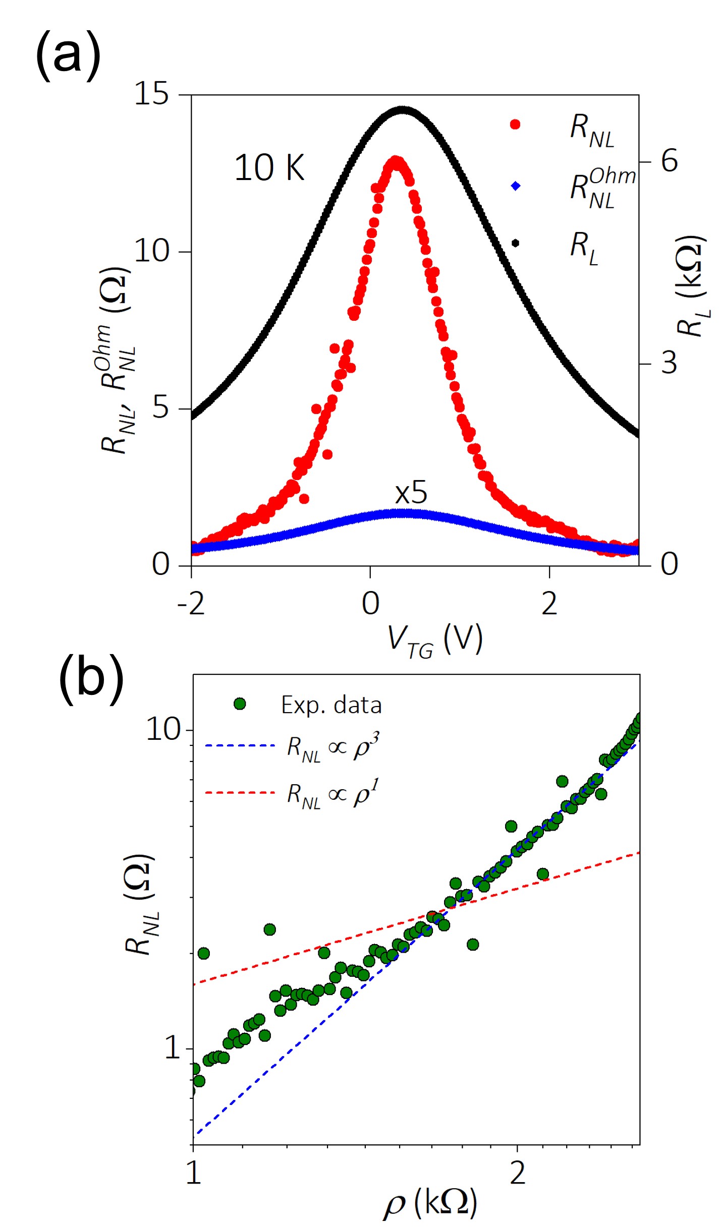
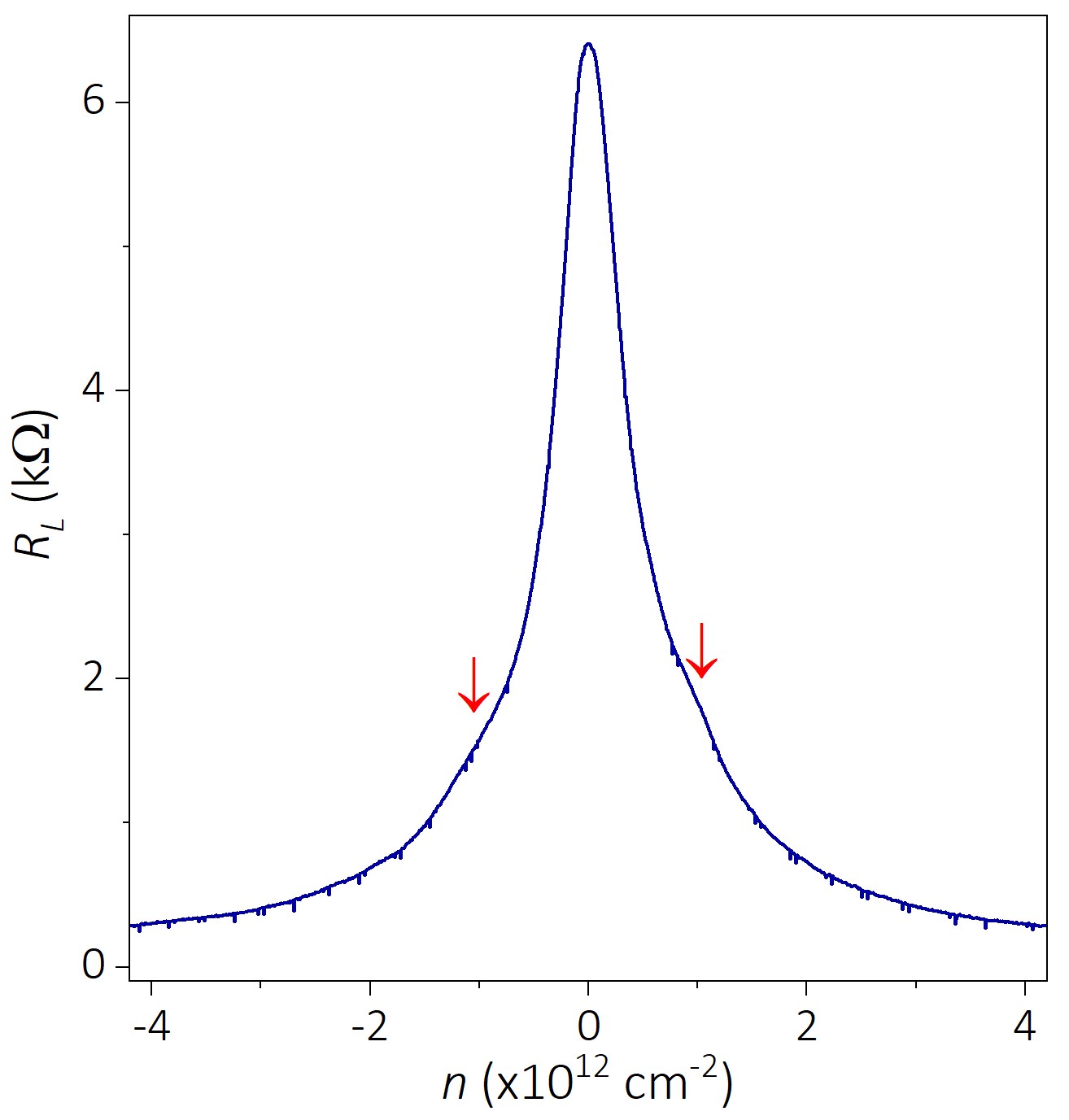
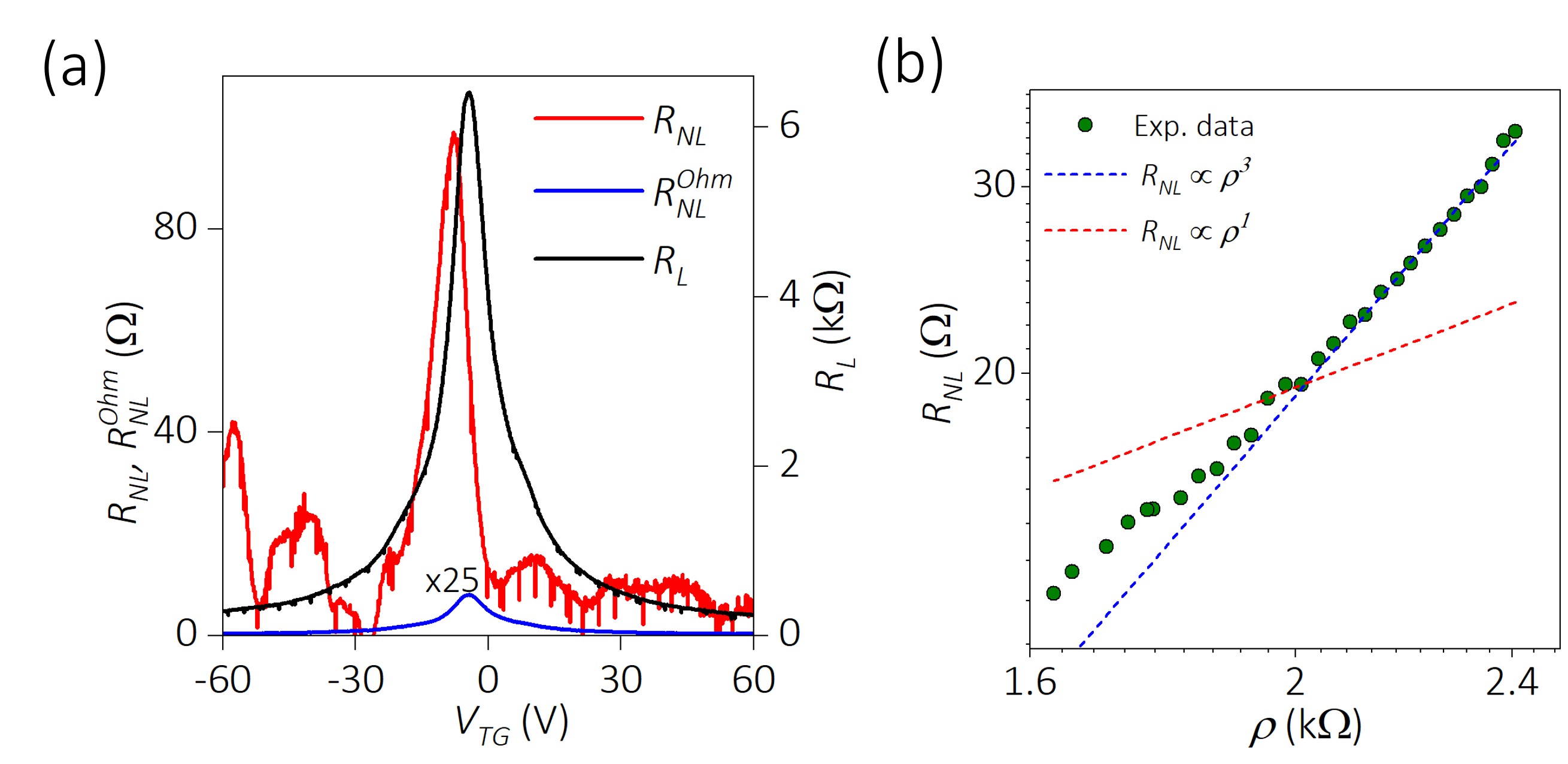
The local and non-local electrical measurements are performed following the standard four-terminal method using KEITHLEY 4200 semiconductor parameter analyzer with a high input impedance (1013 ) at the voltage terminals. A separate source meter (KEITHLEY 2400) is used to apply gate voltage. Figure 2a compares the local () and non-local () resistance measurement results for Device A at 10 K. For , a current is applied between terminal 2 and 3 and the voltage drop between terminals 9 and 8 is detected giving = . For measurement, the current is applied at the local terminals 3 and 8, and the voltage drop at terminals 2 and 9 is measured, giving = . The length and width of the Hall bar in the measured region are 2.5 m and 1 m, respectively. A strong signal is detected around the charge neutrality point (CNP) with zero electric or magnetic field applied across the layers. The peak of the generally appears at the CNP. The shift in the peak is attributed to the in-homogeneity in the bilayer graphene channel, especially since the graphene is on substrate. To rule out the possibility of diffusive charge contribution to the measured non-local signal, we also calculated the Ohmic contribution using the formula Abanin-2011 . The calculated Ohmic contribution is at least one order of magnitude less than that of the measured , thereby ruling out the possibility of diffusive charge contribution. One possible origin of the observed would be the VHE. The Berry curvature induced VHE and the resultant transverse valley Hall conductivity () is related to the measured as
| (1) |
where and are the length and width of the device, is the valley diffusion length and is the conductivity. In the small valley Hall angle regime (), and holds a cubic scaling relation (). Thus we plotted as a function of as shown in figure 2b, which exhibits a clear cubic relation implying that the measured indeed originates from the VHE. Here, is defined as where and are the width and length of the measured part of the channel, respectively.
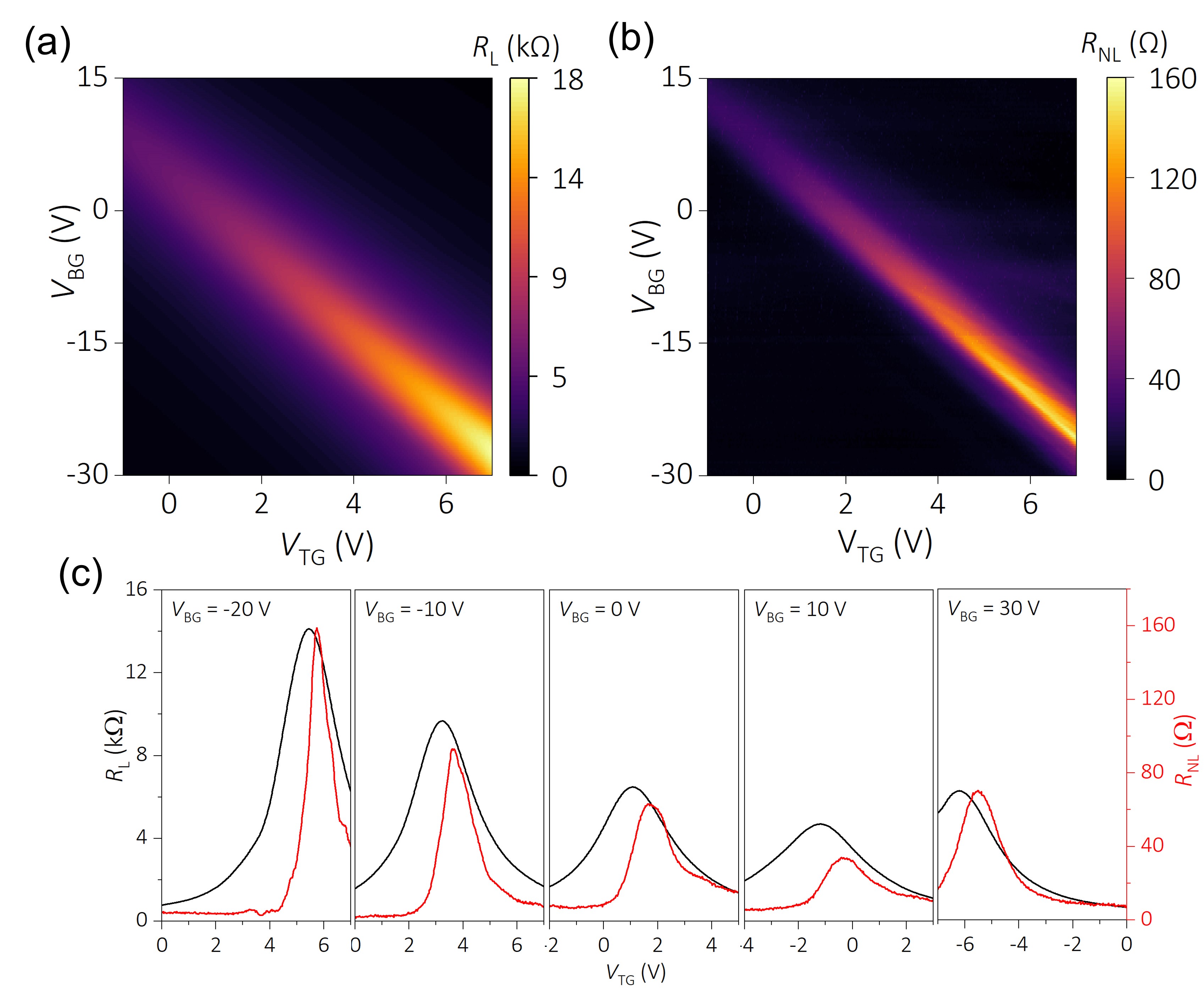
Next, we investigate the effect of an electric displacement field applied across the bilayer graphene on both and . Figure 3a and b show the heat map of the and respectively as a function of both top-gate and bottom-gate voltage. It can be seen that the is narrower than indicating the difference in the physical origin of both peaks. Applying voltages on the top and bottom gates allows the independent control of carrier concentration and the displacement field. The displacement fields related to the top and bottom gates ( and ) are defined as:
| (2) |
where and are the dielectric constant and thickness of the top(bottom) layer. is the voltage offset, which is -1.2 V and 10 V respectively, for Device A. The difference between the two displacement fields gives the carrier doping, and the average of the two is the net displacement fields. Figure 3c shows the evolution of and as a function of the displacement field. Here and are plotted as a function of top gate voltage with the back gate fixed at different values. As mentioned earlier, the heterostructure at the pristine state () shows a clear non-local signal, suggesting an in-built asymmetry present in the heterostructure. Application of a negative electric field ( = -20V and -10V) increases the intensity of both and . This implies that a negative electric field widens the band gap and enhances the asymmetry between the layers. Whereas the application of a small positive electric field () reduces the intensity of both peaks, suggesting a reduction in the band gap and the asymmetry. However, the application of a strong positive electric field () yet again increases the intensity of both and , implying an increase in band gap and asymmetry of the heterostructure.
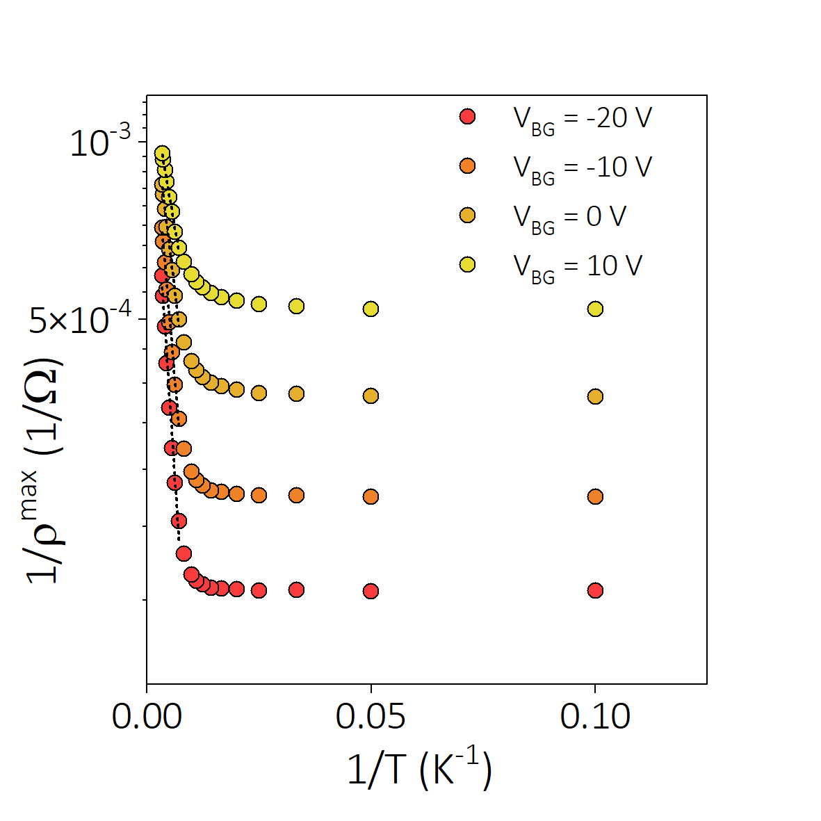
To validate the above hypothesis, we measured the temperature dependence of the at different gate voltages to calculate the band gap. The maximum of the local resistivity () at the high-temperature regime is related to the band gap as:
| (3) |
where is the local resistivity, is the activation energy, is the Boltzmann constant and is the temperature. The band gap , defined as 2, can be extracted by plotting as a function of as shown in figure 4. The dotted line is the fit to equation 3 at the high-temperature regime. Table 1 shows the extracted band gap values at different . The heterostructure has an intrinsic band gap of 25 meV (at = 0 V). Application of a negative displacement field enhances the band gap (35.3 meV at = -10 V and 45.5 meV at = -20 V). At the same time, the application of a positive displacement field reduces the band gap (17.5 meV at = 10 V). This is consistent with the earlier observation of increase(decrease) in the and peak intensity at negative(positive) displacement field.
| (V) | (V/nm) | Band gap (meV) | |
|---|---|---|---|
| -20 | -0.44 | 45.5 | 160 |
| -10 | -0.30 | 35.3 | 94 |
| 0 | 0.14 | 24.8 | 64 |
| 10 | 0.00 | 17.5 | 34 |
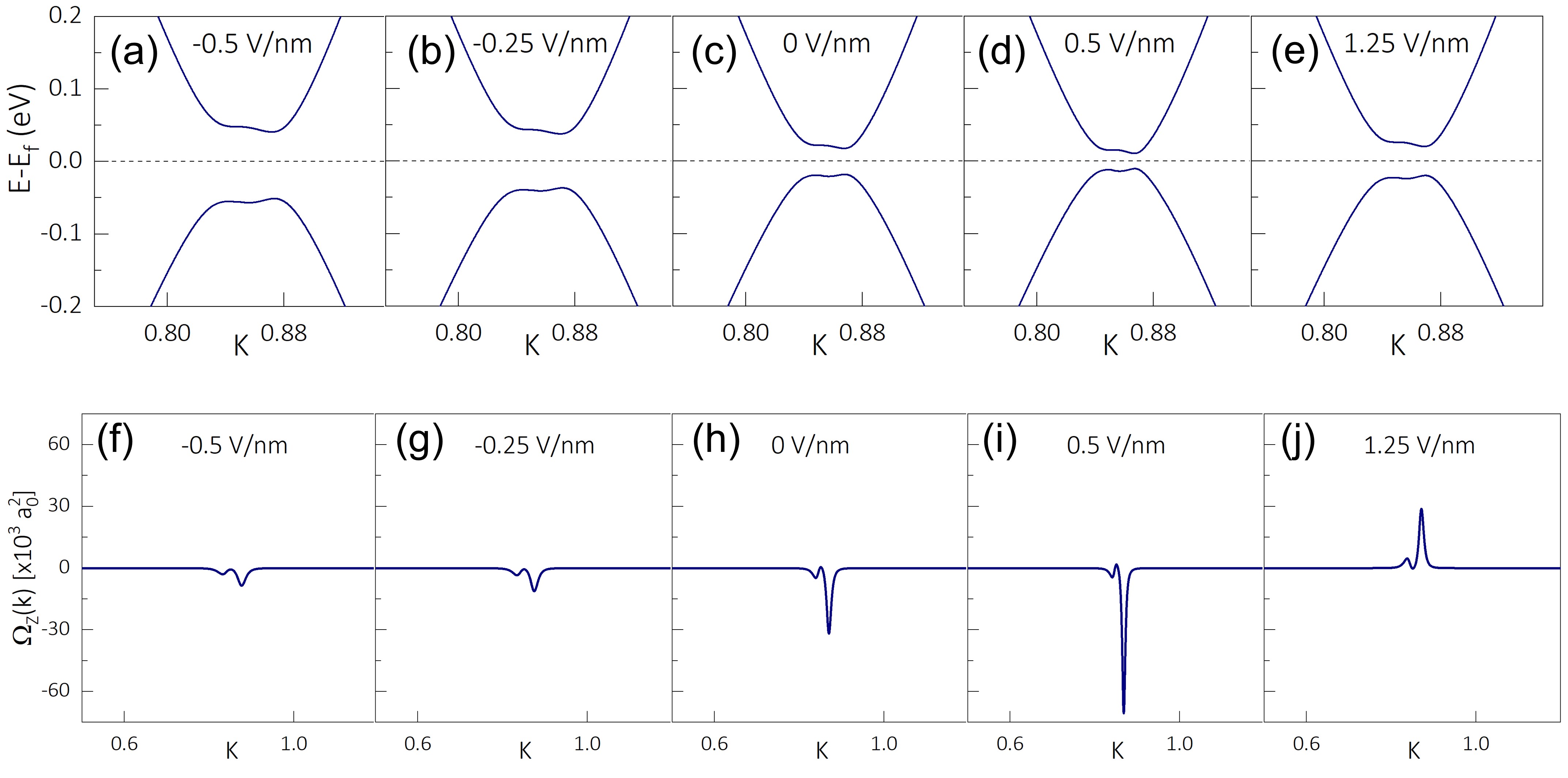
We have also performed ab initio calculations to substantiate the experimental observations (see dft for calculation details). Figure 5a-e shows the electronic band structure calculated for the hBN/bilayer graphene heterostructure at different electric fields applied across the layers. The heterostructure has an intrinsic band gap of 36 meV (Fig. 5c), implying asymmetry between the layers. As the low energy bands are constituted by the non-dimer atoms in the bottom and top layers of the bilayer graphene, the hBN induces different potentials between them, which opens a band gap. Applying a negative electric field (Fig. 5a-b) introduces additional asymmetry between the layers, enhancing the band gap (75 meV for -0.25 V/nm and 92 meV for -0.5 V/nm). However, applying a positive electric field initially works against the inbuilt asymmetry between the layers, reducing the band gap to 21 meV (Fig. 5d). At higher positive electric fields, the electric potential surpasses the intrinsic potential difference between the layers and widens the band gap further (40 meV for 1.25 V/nm), as shown in figure 5e. The results of the band structure calculation strongly agree with the experimental observations. Next, we look at the Berry curvature calculated for the heterostructure. Berry curvature for an electronic band is defined as
| (4) |
where is the periodic part of the Bloch function, is the momentum operator, is the energy of the th band and represents the energy of all other bands. The total Berry curvature is the sum of the individual occupied band’s Berry curvature (). The Wannier interpolation scheme dictates that a pair of bands that are either occupied or unoccupied have a negligible contribution to the total Berry curvature X-Wang-2006 . The major contribution to the total Berry curvature comes from a pair of bands where one is occupied and another unoccupied, such as the low energy bands in the hBN/bilayer graphene heterostructure. In addition, the denominator of equation 4 suggests that Berry curvature value varies as the square of the energy difference between two adjacent bands. Thus in our case, the Berry curvature changes with the electric field as the band gap changes. The heterostructure has an intrinsic non-zero Berry curvature as shown in figure 5h. A negative electric field reduces the magnitude of the Berry curvature as it widens the gap between the low energy bands (Fig. 5f-g). On the other hand, a small positive electric field (0.5 V/nm) enhances the magnitude of the Berry curvature due to the narrow band gap (Fig. 5i). However, two key differences could be observed at a higher positive electric field (Fig. 5j). One, the magnitude of the Berry curvature reduces owing to the widening of the band gap. The second is the change in the polarity of the Berry curvature, which implies that the polarity of the layer asymmetry switches direction at higher positive electric fields.
In conclusion, we have observed Berry curvature induced VHE in non-encapsulated hBN/bilayer graphene heterostructure where the hBN and bilayer graphene are aligned with near-zero twist angle. The VHE is detected as a non-local resistance near the CNP. The cubic relation observed between and validates that the measured indeed originates from the VHE. The measured could be manipulated with the application of a displacement field across the layers, which is attributed to the change in the electronic band structure and the asymmetry of the bilayer graphene under a displacement field. The intrinsic band gap of the heterostructure and its evolution under the displacement field is confirmed from the temperature-dependent measurement in the high-temperature regime. The experimental observations were substantiated with ab initio calculations which showed that the heterostructure has an intrinsic band gap and a non-zero Berry curvature, both of which could be controlled by a perpendicular electric field.
Acknowledgements: Part of this research was supported by Toshiba electronic devices & storage corporation’s academic encouragement program.
References
- (1) John R. Schaibley, Hongyi Yu, Genevieve Clark, Pasqual Rivera, Jason S. Ross, Kyle L. Seyler, Wang Yao, and Xiaodong Xu, Valleytronics in 2D materials. Nature Reviews Materials 1, 16055 (2016).
- (2) Steven A. Vitale, Daniel Nezich, Joseph O. Varghese, Philip Kim, Nuh Gedik, Pablo Jarillo-Herrero, Di Xiao, and Mordechai Rothschild, Valleytronics: Opportunities, Challenges, and Paths Forward. Small 14, 1801483 (2018).
- (3) Xiaodong Xu, Wang Yao, Di Xiao, and Tony F. Heinz, Spin and pseudospins in layered transition metal dichalcogenides. Nature Physics 10, 343-350 (2014).
- (4) Matthew Yankowitz, Jiamin Xue, Daniel Cormode, Javier D. Sanchez-Yamagishi, K. Watanabe, T. Taniguchi, Pablo Jarillo-Herrero, Philippe Jacquod, and Brian J. LeRoy, Emergence of superlattice Dirac points in graphene on hexagonal boron nitride. Nature Physics 8, 382-386 (2012).
- (5) C. R. Woods, L. Britnell, A. Eckmann, R. S. Ma, J. C. Lu, H. M. Guo, X. Lin, G. L. Yu, Y. Cao, R. V. Gorbachev, A. V. Kretinin, J. Park, L. A. Ponomarenko, M. I. Katsnelson, Yu. N. Gornostyrev, K. Watanabe, T. Taniguchi, C. Casiraghi, H-J. Gao, A. K. Geim, and K. S. Novoselov, Commensurate–incommensurate transition in graphene on hexagonal boron nitride. Nature Physics 10, 451-456 (2014).
- (6) Justin C. W. Song, Polnop Samutpraphoot, and Leonid S. Levitov, Topological Bloch bands in graphene superlattices. PNAS 112, 10879-10883 (2015).
- (7) Matthew Yankowitz, Qiong Ma, Pablo Jarillo-Herrero, and Brian J. LeRoy, van der Waals heterostructures combining graphene and hexagonal boron nitride. Nature Reviews Physics 1, 112-125 (2019).
- (8) R. V. Gorbachev, J. C. W. Song, G. L. Yu, A. V. Kretinin, F. Withers, Y. Cao, A. Mishchenko, I. V. Grigorieva, K. S. Novoselov, L. S. Levitov, and A. K. Geim, Detecting topological currents in graphene superlattices. Science 346, 448-451 (2014).
- (9) Katsuyosih Komatsu, Yoshifumi Morita, Eiichiro Watanabe, Daiju Tsuya, Kenji Watanabe, Takashi Taniguchi, and Satoshi Moriyama, Observation of the quantum valley Hall state in ballistic graphene superlattices. Science Advances 4, eaaq0194 (2018).
- (10) Yang Li, Mario Amado, Timo Hyart, Grzegorz. P. Mazur, and Jason W. A. Robinson, Topological valley currents via ballistic edge modes in graphene superlattices near the primary Dirac point. Communications Physics 3, 224 (2020).
- (11) Edward McCann, Asymmetry gap in the electronic band structure of bilayer graphene. Physical Review B 74, 161403(R) (2006).
- (12) Hongki Min, Bhagawan Sahu, Sanjay K. Banerjee, and A. H. MacDonald, Ab initio theory of gate induced gaps in graphene bilayers. Physical Review B 75, 155115 (2007).
- (13) Jeroen B. Oostinga, Hubert B. Heersche, Xinglan Liu, Alberto F. Morpurgo, and Lieven M. K. Vandersypen, Gate-induced insulating state in bilayer graphene devices. Nature Materials 7, 151-157 (2007).
- (14) Yuanbo Zhang, Tsung-Ta Tang, Caglar Girit, Zhao Hao, Michael C. Martin, Alex Zettl, Michael F. Crommie, Y. Ron Shen, and Feng Wang, Direct observation of a widely tunable bandgap in bilayer graphene. Nature 459, 820-823 (2009).
- (15) C. R. Dean, L. Wang, P. Maher, C. Forsythe, F. Ghahari, Y. Gao, J. Katoch, M. Ishigami, P. Moon, M. Koshino, T. Taniguchi, K. Watanabe, K. L. Shepard, J. Hone, and P. Kim, Hofstadter’s butterfly and the fractal quantum Hall effect in moiré superlattices. Nature 497, 598-602 (2013).
- (16) Mengqiao Sui, Guorui Chen, Liguo Ma, Wen-Yu Shan, Dai Tian, Kenji Watanabe, Takashi Taniguchi, Xiaofeng Jin, Wang Yao, Di Xiao and Yuanbo Zhang, Gate-tunable topological valley transport in bilayer graphene. Nat. Phys. 11, 1027 (2015).
- (17) Y. Shimazaki, M. Yamamoto, I. V. Borzenets, K. Watanabe, T. Taniguchi, and S. Tarucha, Generation and detection of pure valley current by electrically induced Berry curvature in bilayer graphene. Nat. Phys. 11, 1032 (2015).
- (18) Kosuke Endo, Katsuyoshi Komatsu, Takuya Iwasaki, Eiichiro Watanabe, Daiju Tsuya, Kenji Watanabe, Takashi Taniguchi, Yutaka Noguchi, Yutaka Wakayama, Yoshifumi Morita, and Satoshi Moriyama, Topological valley currents in bilayer graphene/hexagonal boron nitride superlattices. Applied Physics Letters 114, 243105 (2019).
- (19) E. Arrighi, V.-H. Nguyen, M. Di Luca, G. Maffione, K. Watanabe, T. Taniguchi, D. Mailly, J.-C. Charlier, R. Ribeiro-Palau, Non-identical moiré twins in bilayer graphene. arXiv:2205.01760v2.
- (20) Afsal Kareekunnan, Manoharan Muruganathan, and Hiroshi Mizuta, Manipulating Berry curvature in hBN/bilayer graphene commensurate heterostructures. Physical Review B 101, 195406 (2020).
- (21) L. Wang, I. Meric, P. Y. Huang, Q. Gao, Y. Gao, H. Tran, T. Taniguchi, K. Watanabe, L. M. Campos, D. A. Muller, J. Guo, P. Kim, J. Hone, K. L. Shepard, and C. R. Dean, One-Dimensional Electrical Contact to a Two-Dimensional Material. Science 342, 614-617 (2013).
- (22) Zihao Wang, Yi Bo Wang, J. Yin, E. Tóvári, Y. Yang, L. Lin, M. Holwill, J. Birkbeck, D. J. Perello, Shuigang Xu, J. Zultak, R. V. Gorbachev, A. V. Kretinin, T. Taniguchi, K. Watanabe, S. V. Morozov, M. Andelković, S. P. Milovanovic, L. Covaci, F. M. Peeters, A. Mishchenko, A. K. Geim, K. S. Novoselov, Vladimir I. Fal’ko, Angelika Knothe, and C. R. Woods, Composite super-moire lattices in double-aligned graphene heterostructures. Science Advances 5, eaay8897 (2019).
- (23) Xingdan Sun, Shihao Zhang, Zhiyong Liu, Honglei Zhu, Jinqiang Huang, Kai Yuan, Zhenhua Wang, Kenji Watanabe, Takashi Taniguchi, Xiaoxi Li, Mengjian Zhu, Jinhai Mao, Teng Yang, Jun Kang, Jianpeng Liu, Yu Ye, Zheng Vitto Han, and Zhidong Zhang , Correlated states in doubly-aligned hBN/graphene/hBN heterostructures. Nature Communications 12, 7196 (2021).
- (24) D. A. Abanin, S. V. Morozov, L. A. Ponomarenko, R. V. Gorbachev, A. S. Mayorov, M. I. Katsnelson, K. Watanabe, T. Taniguchi, K. S. Novoselov, L. S. Levitov, and A. K. Geim, Giant Nonlocality Near the Dirac Point in Graphene. Science 332, 328-330 (2011).
- (25) The ab initio calculations are performed using the SIESTA package, which uses the linear combination of atomic orbitals (LCAO) basis sets soler-2002 . To maintain similar interlayer distance between the layers as the experimental values, van der Waals exchange-correlation functionals were used dion-2004 . A vacuum layer of 25 Åwas used to reduce the interaction between adjacent structures. For all the calculations, a Monkhorst-Pack grid of 40 40 1 and an energy cutoff of 500 Ry were used. Structure optimization was performed until the force between atoms was less than 0.01 eV/Å. The Berry curvature calculation was performed using the WANNIER90 package Pizzi-2020 . A total of 15 Wannier functions were used on a Monkhorst-Pack grid of 40 40 1 to calculate the Berry curvature.
- (26) José M Soler, Emilio Artacho, Julian D Gale, Alberto García, Javier Junquera, Pablo Ordejón and Daniel Sánchez-Portal, The SIESTA method for ab initio order-N materials simulation. J. Phys.: Condens. Matter 14, 2745 (2002).
- (27) M. Dion, H. Rydberg, E. Schröder, D. C. Langreth and B. I. Lundqvist, Van der Waals Density Functional for General Geometries. Phys. Rev. Lett. 92, 246401 (2004).
- (28) Giovanni Pizzi et. al., Wannier90 as a community code: new features and applications. J. Phys.: Condens. Matter 32, 165902 (2020).
- (29) Xinjie Wang, Jonathan R. Yates, Ivo Souza, and David Vanderbilt, Ab initio calculation of the anomalous Hall conductivity by Wannier interpolation. Phys. Rev. B 74, 195118 (2006).
Supplementary Information
I Results obtained from Device B
I. Optical image
Figure S1a shows the optical image of Device B where hBN and bilayer graphene edges are aligned with near-zero twist angle. The dotted line shows the graphene region. The arrow indicates the edges of graphene and hBN, which are aligned. Figure S1b is the optical image of the final device. A leakage current was observed from the top gate on this device. This could be due to the insufficient thickness of the hBN layer. Thus no displacement field measurement was performed on this device.
II. Gate characteristics
Figure S2 shows the gate characteristics of Device B. The extracted field-effect carrier mobility from the linear region around the MDP is 9 400 cm2 V-1 s-1 and 7 100 cm2 V-1 s-1 respectively for the holes and electrons. In addition to the MDP, two SDPs, indicated by arrows, can be seen on both sides of the MDP, affirming the formation of a moire superlattice between hBN and bilayer graphene. The SDPs appear very close to the MDP at a carrier density of 1.05 1012 cm-2. This corresponds to a moire wavelength of 20 nm, much higher than the theoretically predicted maximum value of 13.8 nm. The moire wavelength is derived as Yankowitz2-2012
| (S1) |
where is the lattice mismatch between graphene and hBN, is the graphene lattice constant (0.246 nm), is the rotation angle between graphene and hBN. Considering that the rotation angle is 0, a moire wavelength of 20 nm corresponds to a lattice mismatch of 1.25%, which is smaller than the lattice mismatch between pristine hBN and graphene (1.79%). This implies that the graphene is stretched. We attribute the stretching in graphene to the non-uniform surface of SiO2 as the bilayer graphene is in direct contact with it.
III. Local and non-local measurement results
Figure S3a shows the local () and non-local () resistance for Device B at 10K. The calculated Ohmic contribution to the is negligible compared to the magnitude of the . Figure S3b is the cubic scaling relation plotted between and , where is defined as . The width and length of the measured part of the channel are 1 m and 2.5 m, respectively. The clear cubic relation between and implies that the non-local signal originates from the valley Hall effect.
References
- (1) Matthew Yankowitz, Jiamin Xue, Daniel Cormode, Javier D. Sanchez-Yamagishi, K. Watanabe, T. Taniguchi, Pablo Jarillo-Herrero, Philippe Jacquod, and Brian J. LeRoy, Emergence of superlattice Dirac points in graphene on hexagonal boron nitride. Nature Physics 8, 382-386 (2012).