Process Variation-Aware Compact Model of Strip Waveguides for Photonic Circuit Simulation
Abstract
We report a novel process variation-aware compact model of strip waveguides that is suitable for circuit-level simulation of waveguide-based process design kit (PDK) elements. The model is shown to describe both loss and—using a novel expression for the thermo-optic effect in high index contrast materials—the thermo-optic behavior of strip waveguides. A novel group extraction method enables modeling the effective index’s () sensitivity to local process variations without the presumption of variation source. Use of Euler-bend Mach-Zehnder interferometers (MZIs) fabricated in a 300 mm wafer run allow model parameter extraction at widths up to 2.5 m (highly multi-mode) with strong suppression of higher-order mode excitation. Experimental results prove the reported model can self-consistently describe waveguide phase, loss, and thermo-optic behavior across all measured devices over an unprecedented range of optical bandwidth, waveguide widths, and temperatures.
Index Terms:
Silicon photonics, compact modeling, process variation.I Introduction
Silicon photonics (SiPh) has seen explosive growth in demand as a technology platform, driven by its adoption in data centers (DC), high performance computing (HPC) [1, 2, 3], quantum computing [4, 5, 6, 7, 8], and radio-frequency communication systems [9, 10, 11]. SiPh’s rapid rise and maturation has been enabled by its ability to leverage decades of research in the complementary metal–oxide–semiconductor (CMOS) industry, drastically reducing the typical research and development (R&D) costs associated with new semiconductor technologies [12, 13, 14]. SiPh, however, has not yet been able to mimic CMOS yield prediction tools for evaluating photonic integrated circuits (PICs). Yield is a ubiquitous metric used across semiconductor manufacturing, with improvements in yield being strongly correlated with reductions in the time and costs associated with PIC design cycles [15, 16, 17]. The need for predictive yield models can be mitigated to some degree by designing variation-robust devices [18] or PICs such that performance variations can be tolerated or corrected for post fabrication [19, 20]. In each of these cases, however, quantitative yield data cannot be determined prior to fabrication—an obstacle that will be exacerbated as the number of components per PIC in silicon is projected to scale well into the millions within the next decade [21]. Circuit designers also need tools to optimize system-level performance through device-level design choices [22]. To meet rising circuit design complexity, commercial foundries must develop process design kits (PDKs) that include compact models that are both parameterized over a wide range of relevant design and environmental variables and describe all important device figures of merit [23, 24]. It is essential that strip waveguides in particular—a critical component of most SiPh circuits—are accurately modeled according to their expected fabricated performance.
| Model Features | [25] | [26] | This Work |
|---|---|---|---|
| Wavelength [nm] | 1550 | 1520–1570 | 1450–1650 |
| Nominal Width Range [nm] | 480 | 480–500 | 400–2500 |
| Considered Variation Sources | , | , | Arbitrary |
| Statistical Parameter Variations | ✓ | ✓ | ✓ |
| Waveguide Scattering Losses | ✗ | ✗ | ✓ |
| Thermo-optic Effect | ✗ | ✗ | ✓ |
| - Waveguide Width Variations | |||
| - Waveguide Thickness Variations | |||
Broadly speaking, there are three ways to construct compact models: (i) look up table-based models, obtained directly from measurements or device simulations, (ii) models based on empirical fit functions, and (iii) physics-based models [23]. Most previously reported work falls under the look-up table-based category [27, 26, 25, 28, 29]. These models can be parameterized using look-up tables (LUTs), where interpolation is used to predict the performance of designs not explicitly defined in the table. Ensuring that LUT models are accurate over a wide range of input parameters, however, requires measuring all waveguide figures of merit for every combination of input parameters; a task that scales exponentially with the number of modeled independent variables. Prior demonstrations methods also require the explicit connection of the measured effective and group index variations to a predefined number of process variation sources, introducing the possibility of error if any systemic deviations exist between the simulation configuration and the realities of the fabrication process.
In this paper, we report to the best of our knowledge, the first geometry-parameterized compact model of strip waveguides that can capture device performance over a wide range of wavelengths and waveguide geometries (see Table I). Using a novel derivation of the thermo-optic effect that is accurate for high-index contrast waveguides, we demonstrate our model’s ability to describe both scattering loss and the thermo-optic effect as a function of both design and statistical parameters. A novel group-extraction-based method allows the characterization of process variations without presumption of a source or its associated sensitivity. This extraction methodology is used to construct a model from dozens of geometric variations of Mach-Zehnder Interferometers (MZIs) fabricated in a 300 mm commercial foundry. These use of Euler bends in these MZIs permits the characterization of wide waveguide performance with minimal higher-order mode excitation. Experimental results validate the model’s accuracy in describing the phase, loss, and thermo-optic performance across the entire wafer. The model is also implemented in Verilog-A to demonstrate compatibility with electronic-photonic co-simulation environments [30, 31, 32]. This work represents a key step toward the modeling of waveguide-based PDK components, enabling true-to-measurement circuit simulation at massive integration densities.
II Physics-Aware Model Development
Because the mode condition of an optical waveguide is described via a transcendental equation, completely generalized analytical solutions for the effective index are impossible to derive [33]. We therefore propose, as discussed in [34], finding a behavioral model that accurately captures its dependence on all design parameters over the relevant ranges of interest. In this section, we develop dependency models for the design parameters available. The semi-physical nature of the model is then leveraged to describe both the scattering loss and the thermo-optic coefficient. Process variations, whether of a design parameter or not, will be covered in Section IV.
II-A Wavelength Dependence
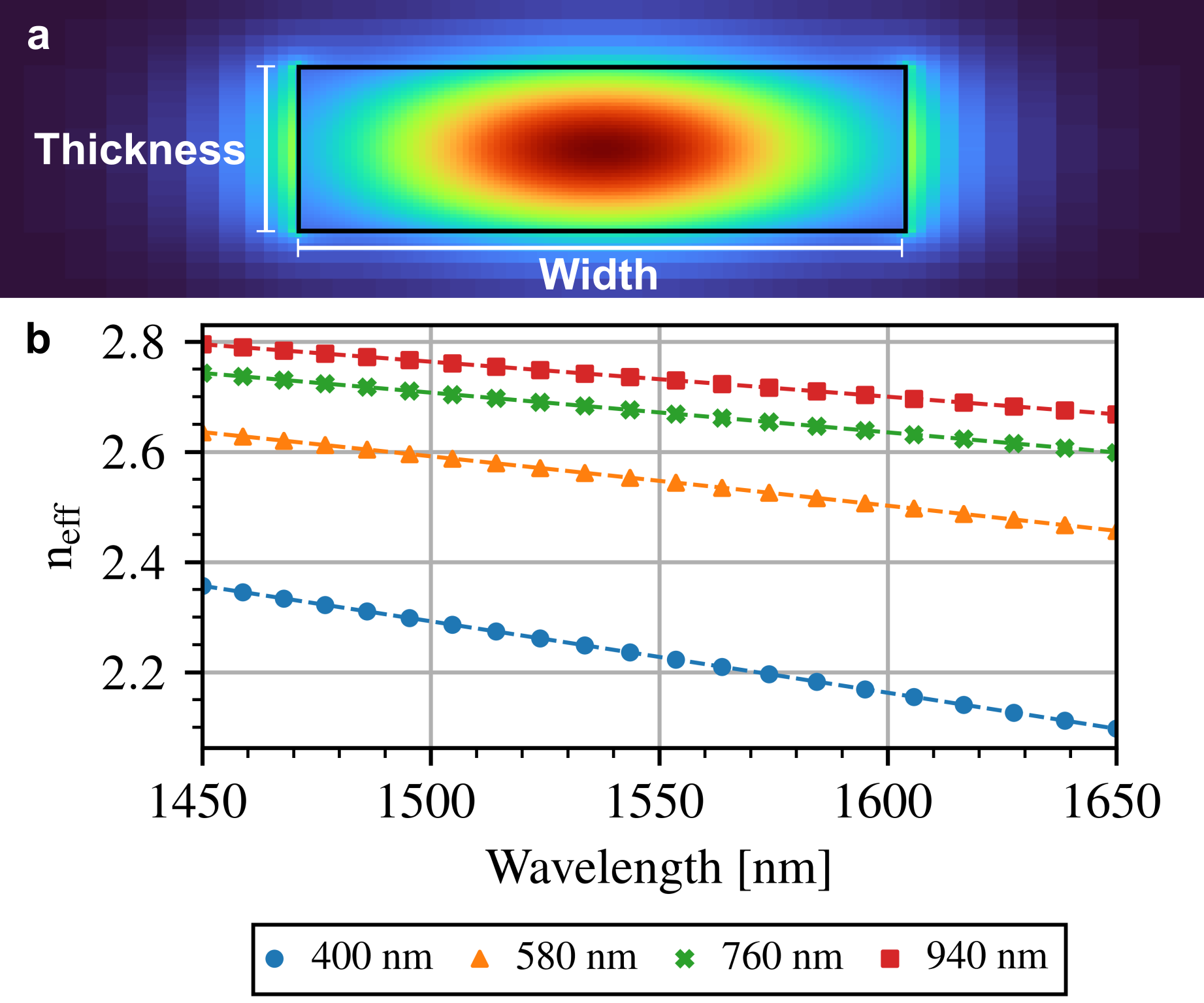
The wavelength dependence of the waveguide is first considered. The of several silicon-on-insulator (SOI) waveguide geometries were simulated in Lumerical MODE (Fig. 1a). From the results, it is shown that the wavelength dependence over the S-, C-, and L-bands for all geometries is well-approximated by a second-order Taylor expansion for a wide range of waveguide widths sufficiently above the cutoff condition (Fig. 1b):
| (1) |
II-B Geometric Dependence
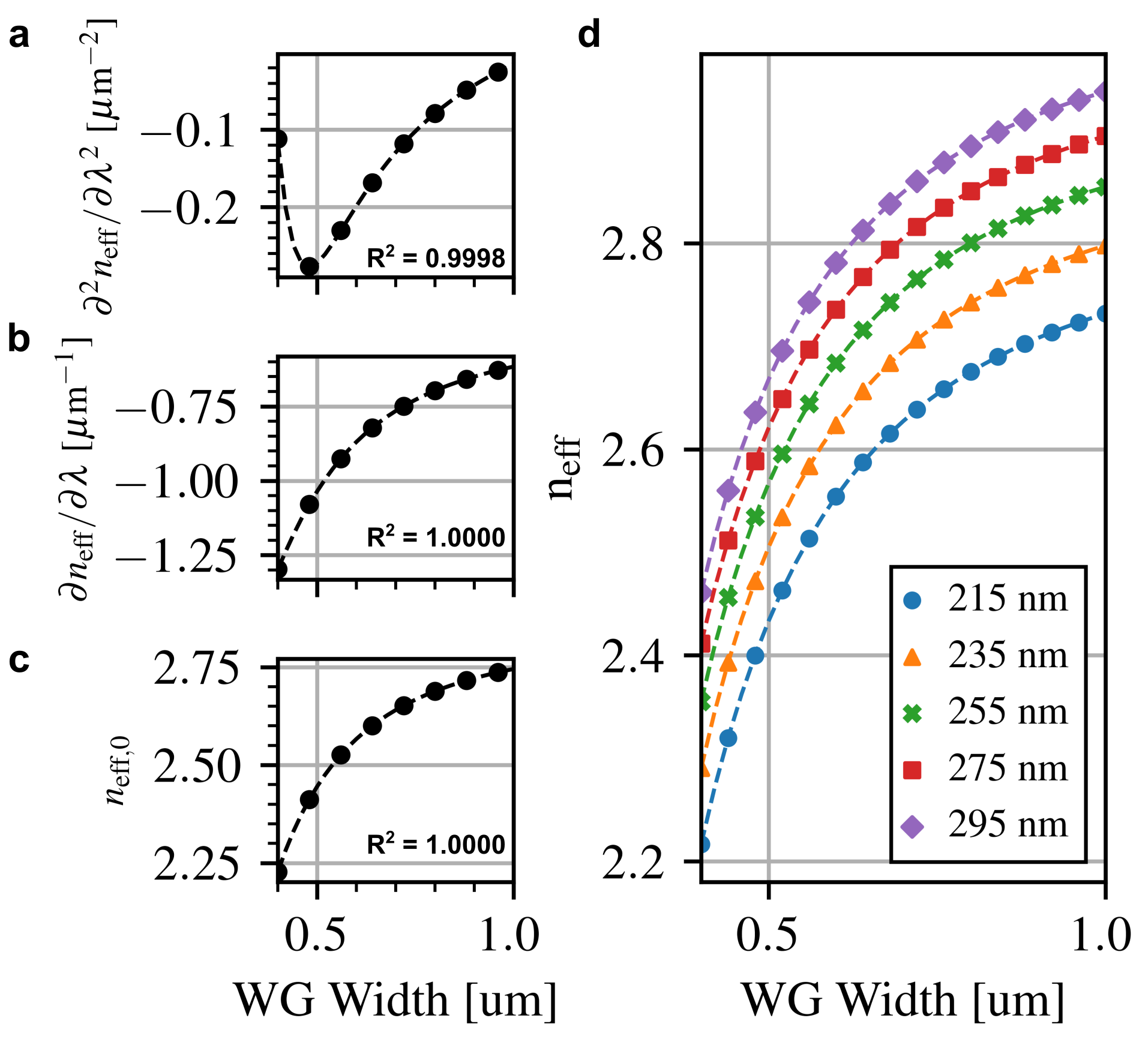
As the Taylor expansion only captures the wavelength-dependence, it is clear that the fitting parameters , and (hereafter referred to as ) are responsible for capturing the dependence on waveguide geometry. With respect to width, all three fitting parameters were previously found in [35] to be well described by the following behavioral model:
| (2) |
for a total of fifteen model parameters. To verify correctness of the model, all three parameters were fitted to the simulation data with (1)-(2) using ordinary least squares (OLS) regression. The model was able to match all three parameters over the entire range of the width sweep (Fig. 2a-c). The close matching of the modeled and extracted Taylor parameters means that our modification of (2) still preserves its ability to match the behavior of effective index as a function of wavelength. By extension, these three Taylor parameters allow for a robust description of as a function of waveguide width (Fig. 2d). The data also demonstrates this agreement is not unique to any particular waveguide thickness, with different thicknesses producing different sub-parameter fits.
Finally, it should be noted that both the numerator and denominator in (2) are polynomials of equal order. Our model consequently predicts that, for a given wavelength, the effective index will asymptotically approach a constant value as approaches infinity. The value that the model approaches as tends towards infinity can be interpreted as the equivalent of an infinite slab of the same thickness:
| (3) |
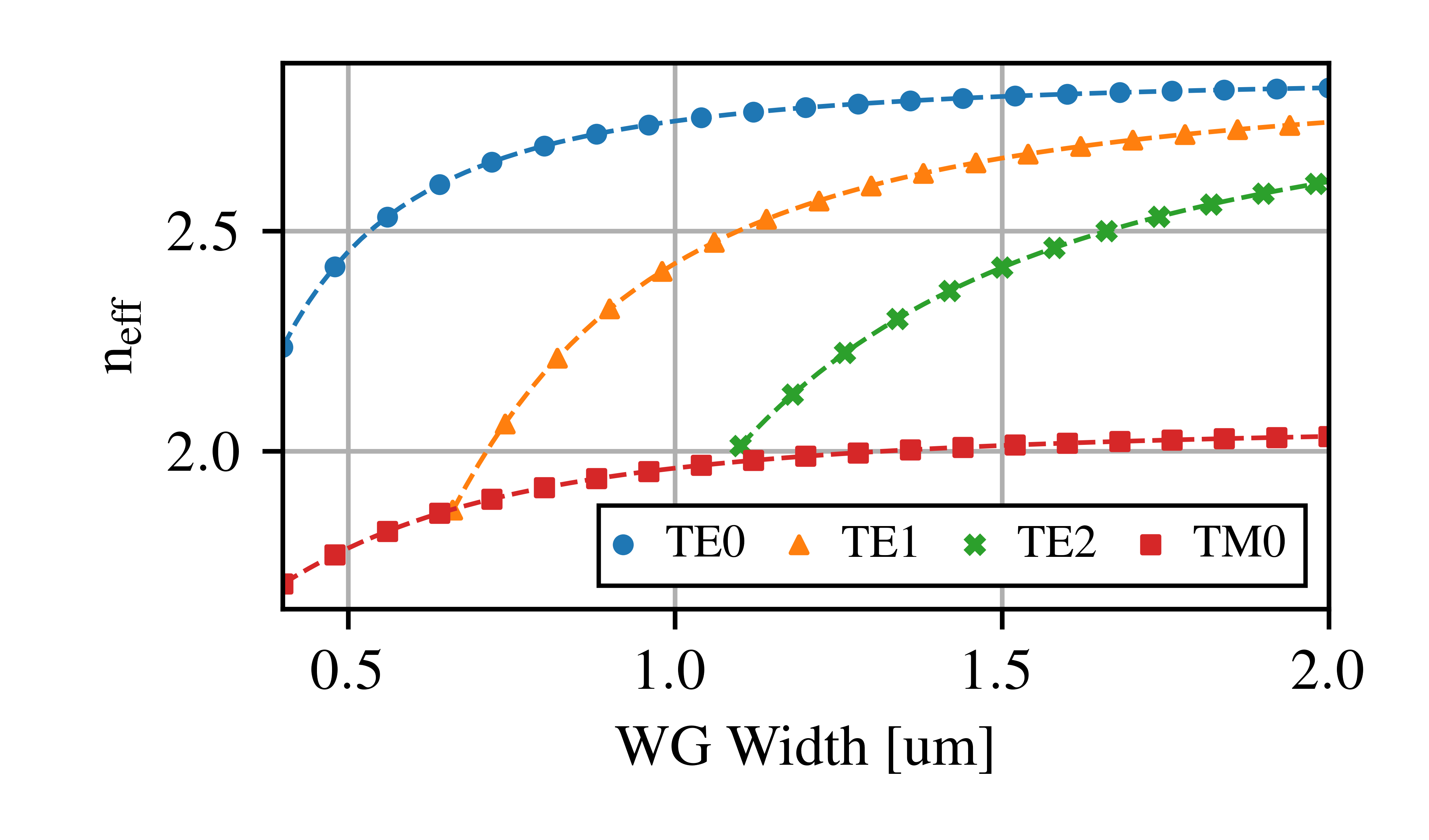
In this way, our behavioral model can elegantly capture all significant features of effective index for the design parameters of interest. The model’s accuracy holds true for higher order modes as well, provided that they are sufficiently far away from their respective waveguide cutoff condition (Fig. 3).
II-C Scattering Loss
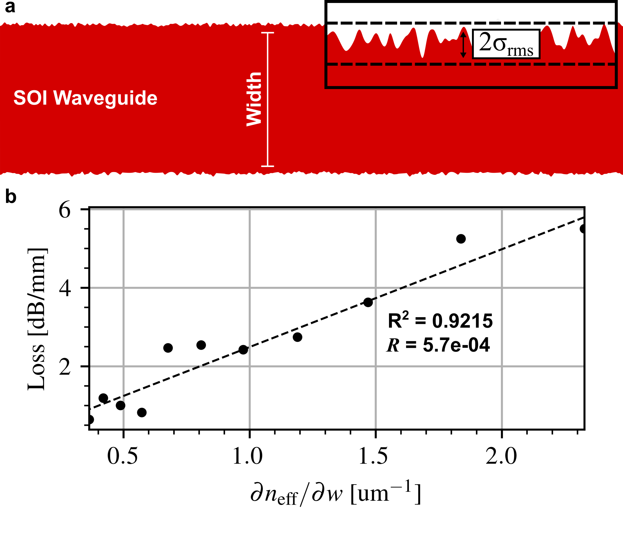
Scattering loss due to sidewall roughness (SWR) can be a significant source of loss in most reported waveguide designs, making it critical for designers to accurately model [36]. In this section, we demonstrate our model’s ability to capture SWR loss as a function of waveguide geometry. It was first noted in [37] that the traditional Payne and Lacey model of SWR-induced loss [38, 39] was found to be identical in behavior to the derivative of the effective index with respect to waveguide width:
| (4) |
where is a proportionality constant. As our model can describe as a function of width, a closed-form representation of can be exactly derived. This equation can then be fitted to measured waveguide loss data to extract the proportionality constant. We validate this by fitting (4) to the scattering loss of a 7 m long SOI waveguide with some SWR wall roughness in Lumerical 3D-FDTD (Fig. 4a). The roughness Root Mean Square (RMS) and correlation length were arbitrarily chosen to be and respectively. These parameters were then used to generate a random, anisotropic SWR on the waveguide walls [40]. Propagation losses were simulated for waveguide widths ranging from 450 nm to 850 nm. The results of the fitting are shown in Fig. 4b, with our model closely matching trend of the scattering loss behavior extracted from FDTD simulations.
II-D Thermo-Optic Effect
Our model can also completely describe the thermo-optic coefficient of an arbitrary waveguide geometry without the need for any thermal measurements. The thermo-optic coefficient of a waveguide mode most importantly requires knowledge of the confinement factor, which is the fraction of a mode’s power confined within each constituent waveguide material. Kawakami showed in [41] that for a waveguide made up of N materials, each with with an index and a confinement factor :
| (5a) | |||
| (5b) | |||
where (5b) is derived from noting that the sum of all confinement factors must equal unity due to power conservation. A closed-form of the confinement factor for a two-material waveguide (e.g. SOI wires) can then be derived:
| (6a) | |||
| (6b) | |||
where is the power contained in the waveguide core and is the power contained in the cladding.
Next, we must obtain an expression that describes the thermo-optic effect on in terms of the confinement factor. A common approximation of the thermo-optic coefficient of is
| (7) |
where represents a small perturbation in the values, is the confinement of the mode within material and is the thermo-optic coefficient of material [42]. Though this equation is widely used [43, 44, 45] and may be accurate in certain scenarios, to the authors’ knowledge it has never been demonstrated to be a generally accurate approximation. We therefore start from first principles and consider a general perturbation of the wave equation [46]:
| (8) |
where is the effective wavenumber, is the confinement in the waveguide core, is the confinement in the waveguide cladding, and and are the core and cladding indices respectively. Carrying this operation through and combining with (1) (see Appendix -A for details) yields:
| (9a) | |||
| (9b) | |||
where is the at some reference temperature . The key addition to (9) compared to prior literature is the scaling of each thermo-optic term by ratio between the material and effective indices. As the index contrast between the core and cladding decreases, our model will approach the (7). Thus it is clear that our model will outperform (7) in accuracy when describing high index contrast materials, such as the SOI waveguide geometries prevalent in SiPh.
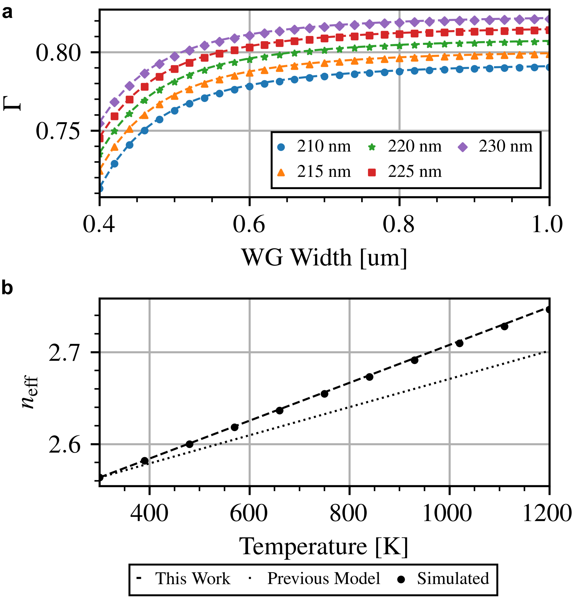
With these expressions, our confinement factor and the thermo-optic coefficient models can be validated. The simulated confinement factor is compared to our model prediction at 1550 nm in Fig. 5a. The optical properties of silicon and silicon dioxide used in our model were taken directly from [47]. There was a near perfect agreement between the modeled and simulated confinement factor, showing that the general behavior of confinement factor is captured by our model (Fig. 5a). The modeled thermo-optic coefficient is validated by simulating how the of a SOI waveguide varies with temperature using Lumerical MODE (Fig. 5b). Silicon was assumed to have a thermo-optic coefficient of K-1 [48] and SiO2 was assumed to have a thermo-optic coefficient of K-1 [49]. The model and simulations show exceptional agreement from 300 - 1200 K, despite the fact that our model does not require any data from thermal simulations or measurements. As predicted, the previously reported model of the thermo-optic effect (7) significantly under-predicts the expected change in . It should be noted that in real devices, waveguide geometry itself is a function of due to thermal expansion. This can be accounted for by modeling as a function of . Experimental results in Section V-C, however, show that assuming a constant width geometry provides sufficient accuracy.
Having a model of the thermo-optic effect that is accurate over a wide range of conditions like this one holds a great deal of potential to enable more robust design exploration, such as evaluating photonic waveguide heater designs [50, 51], characterizing self-heating in micro-resonators [52], or studying the effect of ambient temperature fluctuations in a system.
II-E Parameter Extraction
The practical utility of a compact model is greatly determined by the associated parameter extraction procedure to connect the model to a given foundry process. This is particularly important when developing statistical models, as accurate parameter extraction is the only way to guarantee that process variations are accurately reflected in the model. A popular solution is to leverage the phase-sensitivity of interferometric optical filters—such as Mach-Zehnder interferometers (MZIs), microresonators, or arrayed waveguide gratings (AWGs)—to monitor process variations across a wafer. Regardless of the chosen device, a shared difficulty lies in accurately guessing what particular interference fringe position corresponds to a particular fringe order [53, 26, 25]. Our method is based on the curve-fitting method presented in [25] and [54], with some additional steps described to include waveguide dispersion as an extracted parameter.
The first step in parameter extraction is to characterize the group index () of a fabricated interferometer from a wavelength sweep of the device. To enable this, (1) is rearranged into a more suitable form:
| (10a) | |||
| (10b) | |||
| (10c) | |||
where and are fitting parameters that aggregate the 1 and 0 order terms from (1) respectively. Following the procedure described in [54], it is first noted that the fringe condition of an inteferometric device is described by
| (11) |
where is the phase difference between the interferometry arms, is the path length of the interferometer, is a particular fringe wavelength, and is an integer corresponding to the particular fringe order. To extract our model parameters, a wavelength sweep of the interferometric device is required. Once this is performed, a peak finding algorithm can be used to detect the wavelength of all detected fringes. A function that relates the relative fringe locations to the of the waveguide is now required. This can be done by defining a continuous function that will yield an integer value at each of the detected fringe locations. Let represent the particular fringe order corresponding to an arbitrarily chosen reference fringe located at . The fringe order of any other fringe can be defined relative to this reference as
| (12) |
This continuous function now allows us to redefine the measured fringes into a form suitable for parameter extraction. A reference fringe variable is now defined by letting . Inserting this back into (12) produces:
| (13) |
where each relative fringe is located at an associated wavelength . Using (13), the of the measured device is now directly related to the measured fringe locations. This fitting equation must now be extended to our specific model parameters. The of a waveguide is defined to be
| (14) |
Combining with (10a) yields an expression for in terms of our compact model:
| (15) |
By inserting (15) back into (13), we can derive an OLS regression-compatible expression:
| (16a) | |||
| (16b) | |||
| (16c) | |||
where are explanatory variables. Performing an OLS regression between and gives us two of our three fitting parameters in (10). Finally, can be calculated by combining equations (11) and (10a):
| (17) |
where the only uncertainty is what fringe order corresponds to each measured fringe . Once is determined from (17), (10b) and (10c) can be used to determine the original fitting parameters in (1). It should be noted that each detected fringe (, ) location will yield very small variations in the B value due to resolution-based uncertainty in the exact value for . For a best guess, all values taken from each measured fringe should be averaged together.
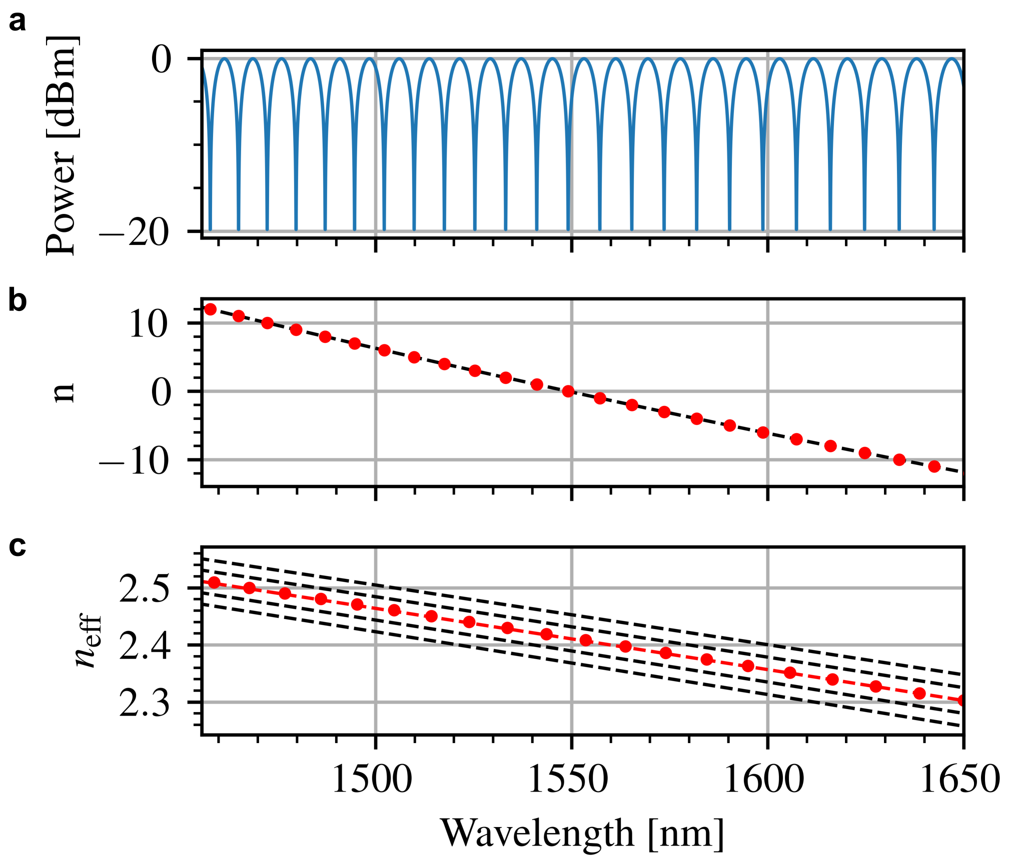
To validate this method under ideal conditions, an MZI constructed using 480 nm x 220 nm waveguides is simulated in Lumerical INTERCONNECT. To ensure accuracy, the waveguide’s was first simulated in MODE and then exported to a MODE Waveguide element in INTERCONNECT. As the full-width half-maximum (FWHM) of the MZI does not affect the extracted , the waveguides were arbitrarily assumed to have a 2.5 dB/cm loss and the coupling coefficient was chosen to ensure critical coupling. The spectrum of the simulated MZI is shown in Fig. 6a. Fringe locations were extracted using a peak finding algorithm. The fringe located closest to the center of the sweep was arbitrarily chosen as . Using (16), OLS regression found m-2 and (Fig. 6b). From here, the family of solutions for is plotted in Fig. 6c. Each particular solution corresponds to a different guess on the fringe orders detected, e.g. vs. . The separation between each solution plotted in 6c is determined by the free-spectral range (FSR) of the interferometer, with a larger FSR corresponding more widely separated solutions.
To determine the correct fringe order of the reference we use the fact that, from the simulations performed in Section II, we know the waveguide geometry has an of 2.411 at the reference fringe location. In Section III we explain how to increase the accuracy of this estimation to avoid errors introduced by this simulation. From this, the reference fringe order is found to be . Since fringe orders must be integer numbers, the result is rounded to the nearest integer 114. By combining (10a)-(10c), the original fitting coefficients are found to be m-1 and . To evaluate accuracy of our extraction, we define the relative error between the extracted and simulated ’s by:
| (18) |
where is the effective index from the MODE simulation, used as a reference to quantify our method’s accuracy, and is the result from applying our extraction method to the simulated MZI. Upon evaluation, the total relative error was found to be 0.017%. Since the order of the reference fringe is correct, the remaining model error is attributed to inaccuracies in the initial regression fit using (16a)-(16c).
III More Robust Extraction Under Process Variability
The reliability of the extraction is highly sensitive to the guessed value of the reference fringe order. For the example in Section II-E, we used a priori knowledge of the at the reference fringe to estimate its order. Therefore, any deviation between the assumed and actual waveguide dimensions risks introducing error. By noting that the initial order estimate rounded to the nearest integer, we can use (11) to define a boundary beyond which our fringe order guess will be incorrect [25]:
| (19) |
We can see that, to raise confidence in the guessed fringe order, either the accuracy of our guess must be increased or the interferometric path length must be decreased. As explained in Section II-E, our extraction method begins by directly extracting the of a given interferometer via optical sweep. Process variations will therefore appear as variations in the extracted values for and . By measuring several devices of the same drawn width across the all measured dies, wafers, and lots, the influence of the random width and thickness variations can be eliminated by averaging their extracted fitting parameters. As the sample size becomes sufficiently large—with the necessary sample size being a function of the severity of the process variations—any remaining deviation between the nominal and averaged parameters will be the result of a systemic etch biases on the waveguide width. We therefore propose estimating this etch bias by creating a preliminary model based on the results of a photonic mode solver, such as Lumerical MODE. Using this model, an equivalent waveguide width can be found by minimizing the error function
| (20) |
where is the extracted model of using the averaged extracted parameters and is the simulation-based, width-dependent a priori model of . The of our equivalent waveguide width can then be plugged into the a priori model to provide a more accurate fringe order estimate. In this way, we can increase the accuracy of our guessed effective index, regardless of whether the modeled waveguide composition is accurate to the virtual device composition.
We now discuss the robustness of this optimization routine in the presence of other systemic non-idealities and its ability to perform etch bias correction. To do this, we need a ’ground truth’ value for , which we obtain by simulating all the non-idealities in Lumerical MODE. Subsequently we perform the parameter extraction using Lumerical INTERCONNECT. By comparing the extracted to the known simulated value for , we can directly evaluate the robustness of our methodology.
III-A Statistical Geometric Variation
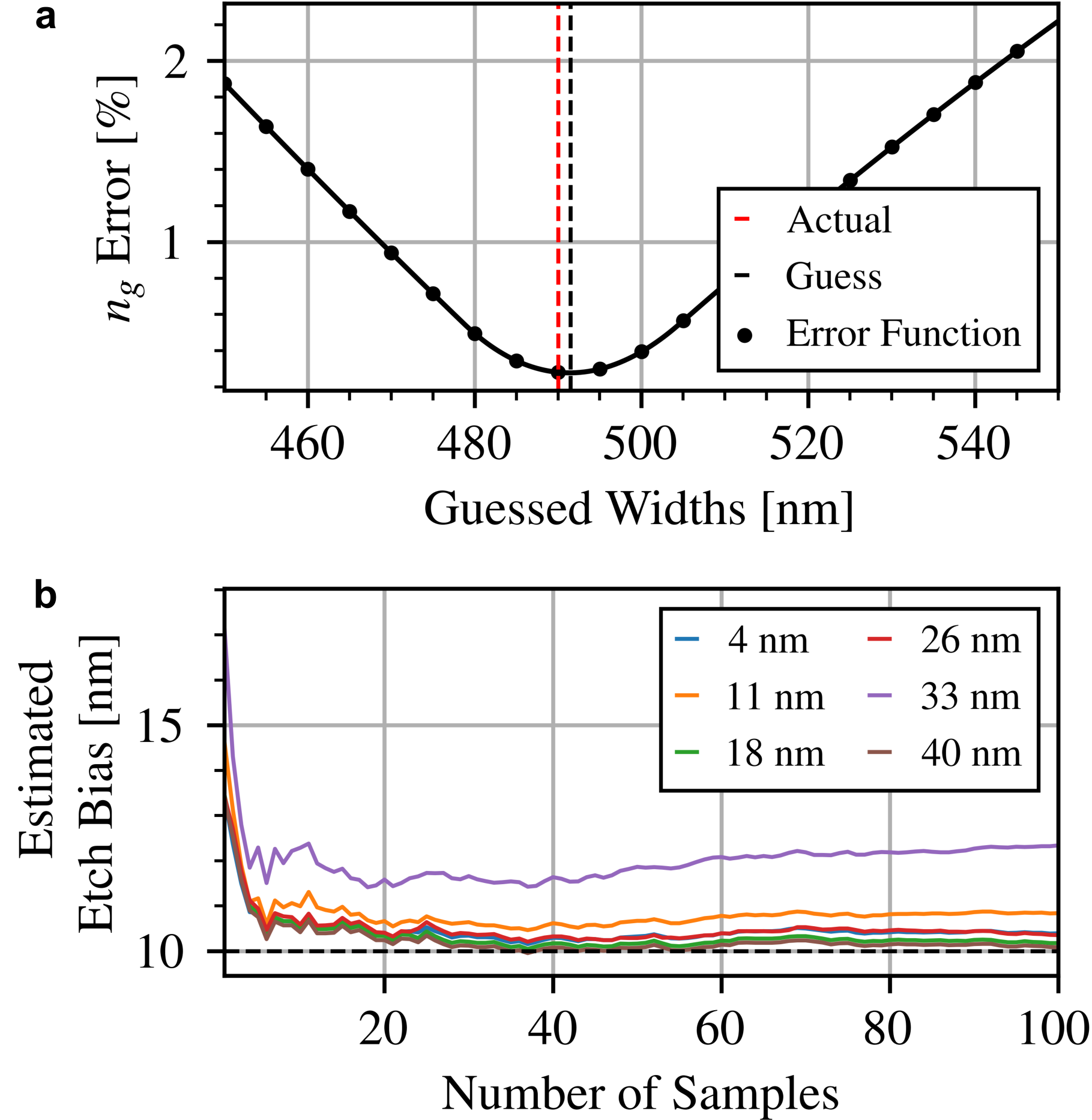
To test the extraction procedure’s accuracy under process variations, a simulation of 100 random variations on the waveguide geometry was run. The nominal waveguide dimensions were assumed to be 480 x 220 nm. To simulate systemic variations, each waveguide was arbitrarily assumed to have an etch bias of +10 nm. Random fluctuations were simulated by subjecting each device to a normally distributed variation of on both the waveguide width and thickness, as this value is consistent with the worst-case reported values for geometric variations [26, 25, 27]. Each mode profile was then exported to INTERCONNECT and simulated with interferometer FSRs ranging from 4 - 40 nm to investigate the effect this had on the extraction error. The resulting error function for one of these samples, with a ground truth width of 490nm, is shown in Fig. 7a. We see the convergence behavior of the etch bias estimate evolves as a function of device sample size increases for several FSR designs in Fig. 7b. It can be seen that all FSR designs can yield at least an estimated etch bias within 2 nm of the actual value, indicating the utility of our etch bias correction.
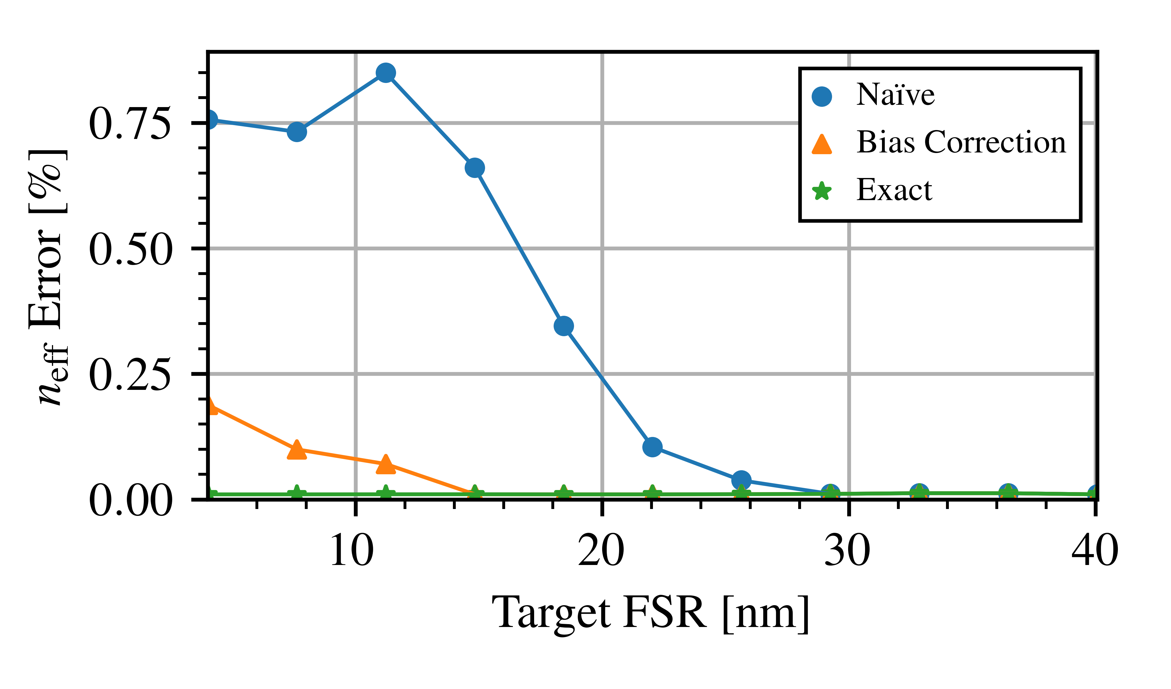
Fig. 8 shows the relationship between the average, per sample error and the interferometer FSR. The error is measured in three scenarios: i.) a ‘naïve’ case, where the fringe order is estimated assuming no etch bias; ii.) where the fringe order is estimated through our etch bias prediction methodology, based on 30 measured samples; and iii.) where the exact from simulations is used to determine the actual fringe orders. The last scenario, that produced an average per sample error of roughly 0.017% represents an error floor for the first two. This error floor is completely determined by errors in the initial regression, as well as any fundamental limitations in our chosen behavioral model. As the FSR is increased, the average per sample error in both cases improves steadily until it reaches the aforementioned floor. This is consistent with (19), indicating that a larger FSR corresponds to a wider margin of error for the fringe order estimate. For both the naïve and bias compensation methods, there is a critical FSR value beyond which the fringe order is correctly estimated for all samples. It is clear, however, that estimating the presence of any etch biases drastically improves the fringe order accuracy, reaching the error floor for a much smaller FSR than when using the naïve method.
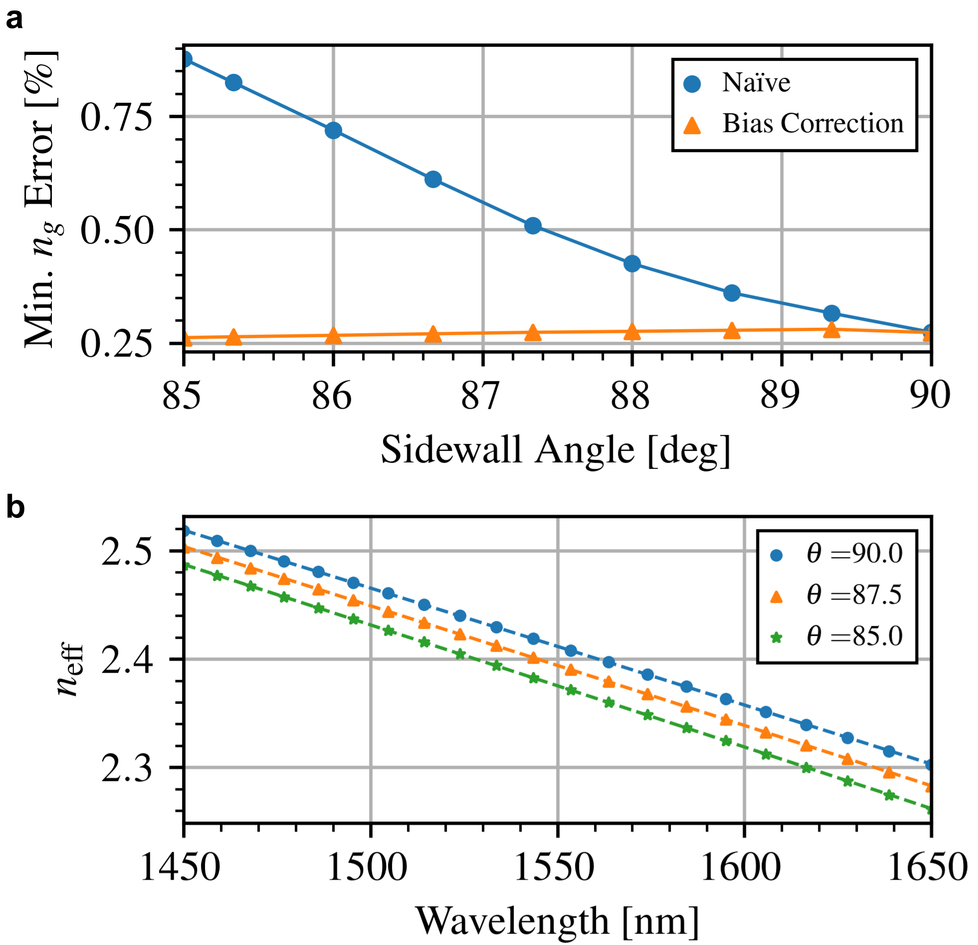
III-B Sidewall Angle
We now consider how the parameter extraction behaves when used for waveguides with some sidewall angle. Up to this point, our simulations assumed the waveguides to have no sidewall angle. Real waveguides, however, typically deviate from this ideal [55]. To study how our bias correction behaves under these conditions, a SOI waveguide with the same nominal (480 x 220 nm) design as before was simulated with a series of sidewall angles from 85 to 90 degrees as this is a range typical of foundries [56, 25]. As only the aggregate behavior is being studied, width and thickness variations were not included. As seen in Fig. 9a, the minimum of the error function optimized in the etch bias estimation step remain roughly constant for all considered sidewall angles. This results in very accurate predictions of the effective index from our model, even though the fundamental geometry is different. We interpret this as our optimization routine is picking an ‘equivalent’ waveguide width that matches the extracted profile. This equivalent width always seems to result in a waveguide design with a similar confinement factor and effective index—and therefore behavior—as seen in Fig. 9b.
III-C Material Variation
This method for increasing the accuracy of the guessed relies on the assumption that the material properties of the fabricated waveguides generally match the assumed material properties used in the simulation data used to construct the model. In practice, however, there can be a great deal of deviation between the assumed and actual optical properties of the waveguide materials. As a workaround, the authors suggest extracting and building a model based around the dispersion of the waveguide , as this waveguide parameter can be extracted exactly from measurements. The nominal model of can then replace in (20) to estimate the width of the measured device. This width can then be used in conjunction with simulation data to assign it an guess. Though the limits of such a technique are unclear to the authors, experimental results in Section V demonstrate to be effective enough for describing the , loss, and thermo-optic effect for all measured device performance.
IV Extracting Local Parameter Variations
Process variations (e.g. thickness variation, cladding and core index variations) will appear in our model as variations in the fifteen model parameters that comprise Eq. (1). Capturing these variations requires the ability to extract their value locally, which cannot be done just by looking at the performance of any individual device. It is commonly assumed in prior literature that most process parameters slowly vary across the entire wafer [25]. This assumption implies that the values of the parameters comprising our model also vary slowly across the wafer. The authors therefore propose analyzing the performance of several waveguide width designs in close proximity to each other to locally extract all of the fifteen model parameters. Each local extraction serves as the observations of each model parameter that are tracked across the entire wafer.
The simplest way to create a statistical model is to treat each of fifteen sub-parameters as independent statistical variables. This is not ideal, however, as each additional variable drastically increases the number of required iterations for accurate Monte Carlo simulations. To minimize model complexity, we would like to represent each sub-parameter as a linear function of an ensemble of variables:
| (21) |
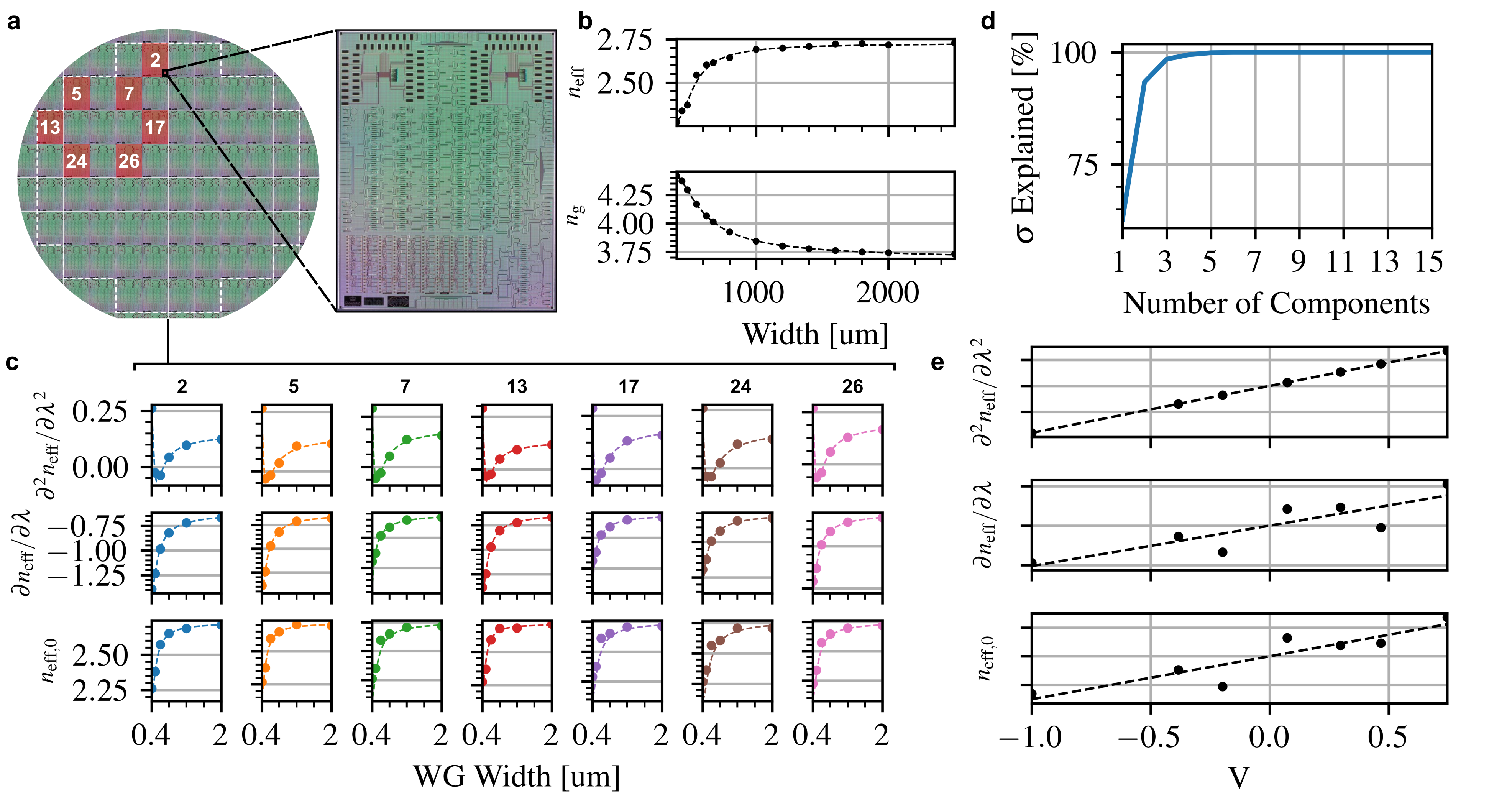
is the vector of variables that represent the process variations. Minimizing model complexity would be the equivalent of minimizing the size of . describes the corresponding sensitivities of a given parameter to each element in . To minimize the size of , we leverage the fact that each extracted model parameter will be strongly correlated to one another. This is because the variations in each model parameter share common origins such as wafer thickness, annealing time, etc. We therefore propose using principal component analysis (PCA), a technique for transforming a number of possibly correlated variables into a smaller number of uncorrelated variables (i.e principal components) [57], to minimize model complexity. The chosen principal components are then the variables that make up . The chosen principal components are then the variables that make up . The number of components in is flexible (see Appendix -B for details). Since our waveguide geometry is primarily a function of two process variables—waveguide width and thickness—we use only the first principal component to preserve its physical interpretation. The result is a model of effective index as a function of width and our process variations–, representing width variations and an additional variable we will call , representing an aggregate of other process variations, including thickness variation:
| (22) |
This full model of is then used in the local optimization and re-extraction of each measured device. The cost function is defined as the sum of the relative and errors to match both the measured fringe locations and FSR respectively.
Thus, we can employ a two-stage direct statistical compact model extraction procedure [24]. In the first stage, we use group extraction to obtain the complete set of fifteen parameters for a uniform device. In a second step, a subset of model parameters are re-extracted for each member of a large ensemble of devices measurements. This approach will be the most accurate representation of how device performance varies across the wafer without any presumption of variation source, statistical distribution, correlation, and the resulting model sensitivity to the variation. An inherent strength of this approach over others is that it is potentially useful for modeling other waveguide geometries as well. This potential is due to the model designer having the option of picking the number of principal components based on a physical assumption on the key process variables or optimize the percentage of explained parameter variance (see Appendix -B). While further investigation would be required to confirm this, the methodology’s flexibility holds a great deal of promise.
V Experimental Demonstration
We measured 7 reticles, each with 135 MZIs consisting of 27 different waveguide widths (w) from 400 nm to 2500 nm and 5 different arm length delays (L) from 100 nm to 500 nm, fabricated on a custom 300 mm full wafer through AIM Photonics (Fig. 10a). All 135 MZI were measured on reticle 2 while a smaller subset of 30 MZIs were measured on each of the remaining reticles, totaling 315 measured devices. Devices with the same waveguide width are placed adjacently to minimize the impact of local process variations on device performance. All MZIs have a nominal waveguide height of 220 nm, and grating couplers designed for quasi-TE polarization are utilized for optical I/O. The two arms of each MZIs consist of symmetric waveguide bends to mitigate the impact of bending on the . For devices with waveguides beyond the single-mode cutoff width, Euler bends are used to maintain single mode operation and high mode isolation [18]. A tunable laser was swept from 1450–1610 nm at a 10 pm resolution to characterize the transmission spectrum of each MZI.
V-A Nominal Extraction
A nominal model is created by averaging the extracted parameters for all measured devices as shown in Fig. 10b. We apply the extraction method described in Section II-E to every collected transmission spectrum. A preliminary model is built using the simulation data described in Section II to estimate the expected device FSR for each waveguide width variation. This estimated FSR is then fed into a peak finding algorithm to extract the parameters, and then estimate fringe orders—and, therefore the —of each measured device. As the measured deviated a great deal from the simulated values, the technique described in Section III-C is employed where a preliminary model based on is created and used to estimate waveguide geometry to estimate the fringe order. All three Taylor-expansion parameters are then derived using (10a)-(10c), and then averaged across for each width variation across the entire wafer to create a nominal experimental model. The extraction is then repeated locally for devices that are close in proximity to one another to extract local values for the model’s sub-parameters (Fig. 10c).
Fig. 10d shows that using (31) this first principal component can explain 62.7% of all variance in the sub-parameter values across the wafer. The authors determined that due to the clear connection between the and the three model parameters that determine device behavior as , this principal component was likely capturing width-independent sources of variance such as thickness variations (Fig. 10e). The authors will now show that this provides a model robust enough for capturing statistical behavior while preserving the goal for clear physical interpretation.
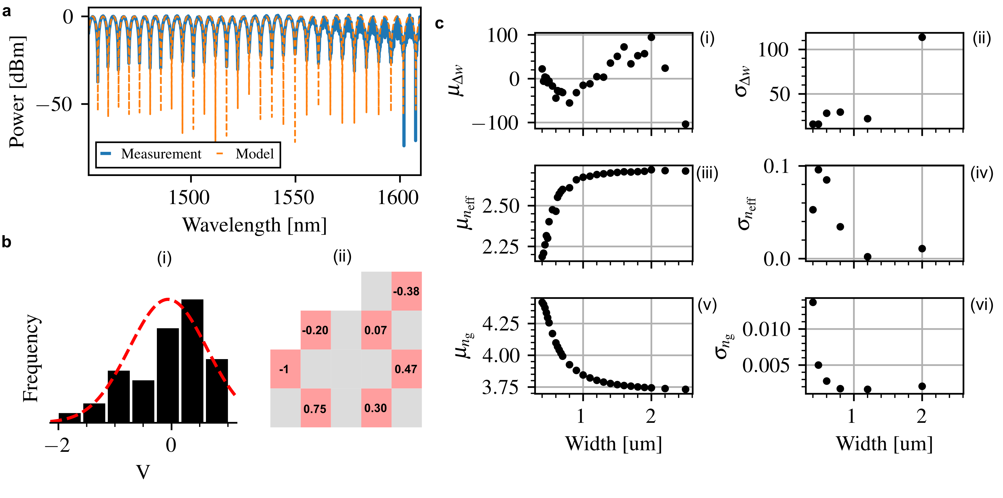
V-B Statistical Extraction
The sum of the relative and errors is optimized using the Nelder-Mead algorithm [58]. The drawn waveguide width and the extracted from the local extraction performed in Fig. 10c are used as the initial guesses for and . Despite the limited sample size of collected data, we can already see several notable preliminary statistical trends in as a result of our model. The model of extracted from each local optimization was found to result in a close agreement between the measured and modeled MZI performance. The extracted values for exhibits the intended physical behavior of process parameter that varies slowly across the wafer (Fig. 11b). Local optimization yielded a total, average intra-die, and average local device standard deviation of 0.603, 0.386, and 0.167 respectively, showing a correlation between device proximity and their extracted values. The mean values of for die both (i) in close proximity to each other and (ii) equidistant from the center of the wafer tend to be similar in value, as shown in the inset of Fig. 11b.
Decoupling the process variations of from the width variations enables extraction of width-dependent systemic effects, as shown in Fig. 11c(i). Our method estimates that waveguide widths with smaller mean errors also tend to have smaller (Fig. 11c(ii)). This carries over as an explanation for why for m, varies more than for m, allowing insight on what waveguide geometry best minimizes both and . This sort of process insight for circuit designers is only possible due to the group benchmarking of all device performance within a localized area.
V-C Thermo-optic Effect Model Validation
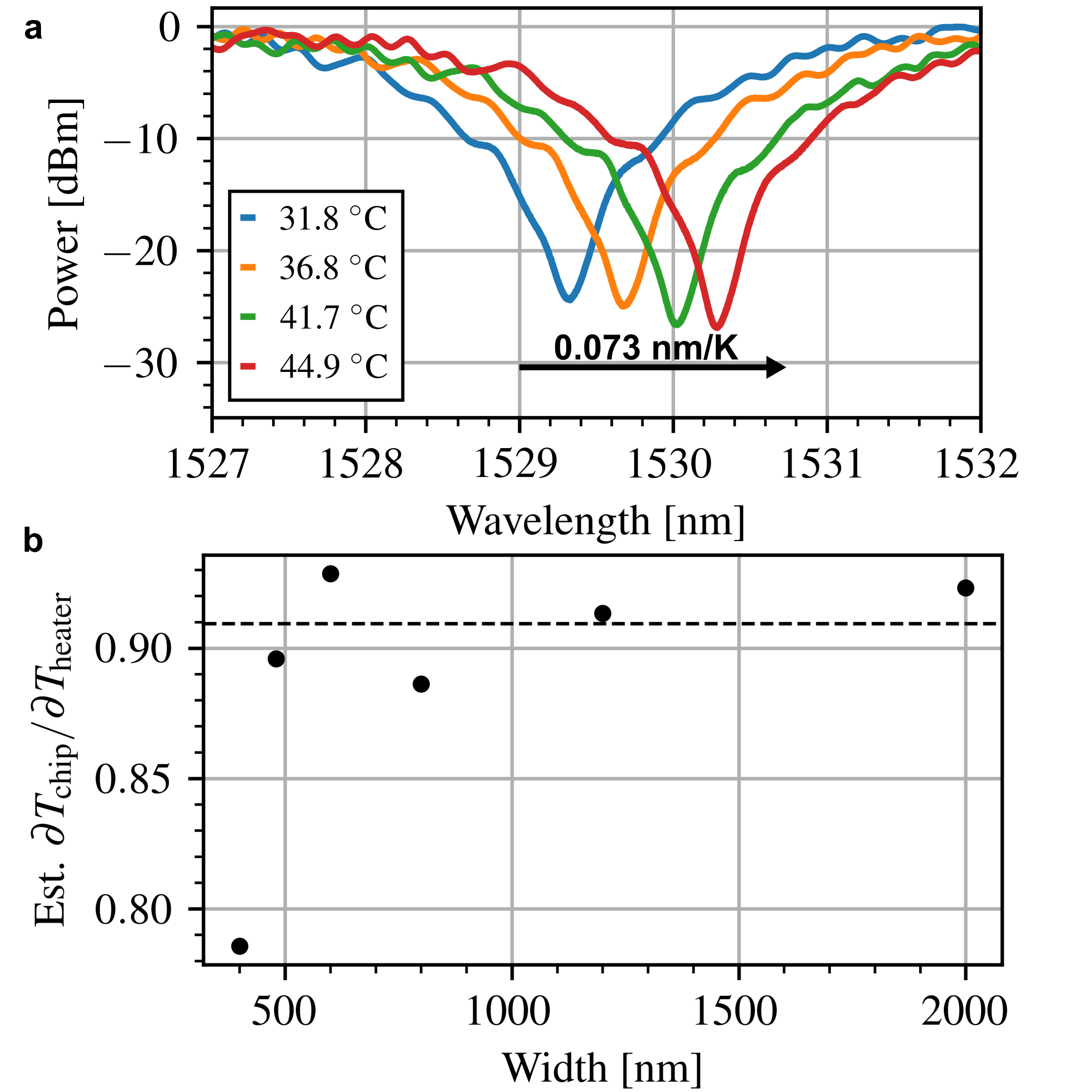
To validate the thermo-optic effect model developed in Section II-D, we re-characterized the MZI transmission spectra from a single die of the chip shown in Fig. 10a. The thermal characterization was performed by adhering a Thorlabs TLK-H polyimide heater to the side of the chip stage. The heater was controlled by a Thorlabs TC200 Temperature Controller to set the heater temperature. Thermal paste was applied between the chip and the chip stage to minimize thermal resistance between the chip and the heater. The thermal response of one of the tested MZI is shown in Fig. 12. The fringe closest to 1550 nm is tracked at each temperature step and plotted against temperature to extract . This value is then compared to our predicted value for gained by taking the derivative of in (11) with respect to temperature

| (23) |
where is the order of the tracked fringe, is the path length difference between the two arms, and represents the heat transfer efficiency from the heater to the chip itself. This last term is included as the authors only know the temperature of the resistive heater rather than the chip temperature itself. We know as heater cannot raise the temperature of the chip to a value higher than its own. The extracted parameters for and are used in calculating (23).
On average, the measured thermo-optic effect was found to be 0.91 our model’s (9) prediction. This value was found to be independent of waveguide geometry with the exception of 400 nm (Fig. 12b). This error for 400 nm is assumed to be because this width is close enough to the cutoff condition for our model to lose accuracy. In contrast, the measured thermo-optic effect was 1.21 the previously reported model’s prediction. This implies that either the chip’s change in temperature is greater than the heater’s or the previously reported model is incorrect. The change in temperature of the PIC can only ever be smaller than the heater’s temperature delta, making the old model’s prediction clearly nonphysical.
V-D Scattering Loss Model Validation
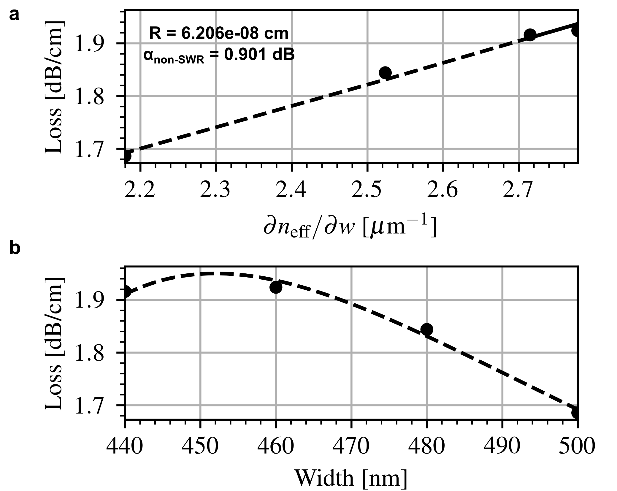
To validate the scattering loss model, we measured a die with 25 spiral loss structures consisting of 5 different waveguide widths (w) from 400 nm to 500 nm and 5 different spiral lengths (L) from 1 cm to 5 cm, fabricated on a custom 300 mm full wafer through AIM Photonics (Fig. 13). Again, all spiral structures have a nominal waveguide height of 220 nm, and grating couplers designed for quasi-TE polarization are utilized for optical I/O. The losses of each spiral length were recorded, and then fit to a linear equation. The slope of the this fit was taken to be the propagation loss associated with each waveguide width. The results of our model fit are shown in Fig. 14. The model built in Section V-B was used to build a model of . Fitting our modeled to the measured propagation loss yields proportionality constant of cm and (Fig. 14a). The intercept of the loss fit is interpreted as the aggregate non-SWR loss, with a value of 0.901 dB. Fig. 14b shows the excellent agreement between our model and the data, predicting the similar propagation losses of both the 440 nm and 460 nm waveguides. As mentioned in Section V-B, both 400 and 420 nm waveguide widths are likely near the cutoff condition. Since (4) is only valid sufficiently far away from this condition, those data points are not included in the plot.
V-E Verilog-A Implementation
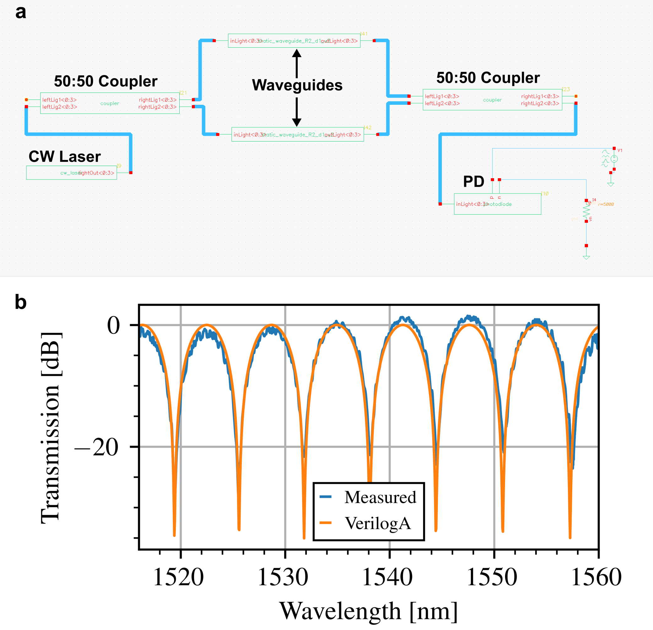
To demonstrate its compatibility with electronic-photonic co-simulation, the circuit model was implemented in Verilog-A within Cadence Virtuoso (Fig. 15a). As Verilog-A does not inherently support optical signals, some compatibility code as well as a small library of photonic device models were built based upon on previously reported demonstrations [59, 32, 60].
VI Conclusion
In summary, we have demonstrated a novel compact model that can greatly expand the accuracy of circuit-level simulation capabilities of silicon PICs. In contrast to prior work that focused on providing metrology information that could be use to fabrication engineers [61, 26, 62], we present this PDK model as a tool suitable for true-to-measurement circuit simulation and optimization. By leveraging this underlying physical behavior and locally extracting process variations by performing group extraction, we have demonstrated a framework for building a model of that is entirely driven by measurement data. This model was shown to accurately describing the phase, loss, and thermo-optic behavior of the measured integrated waveguides over 4 the optical bandwidth and over 80 the range of waveguides widths reported in prior work. We envision that the advancement over prior demonstrations this work represents can support the development of waveguide-based PDK components and enable the robust optimization of next generation PICs.
VII Acknowledgements
This work was supported in part by the U.S. Advanced Research Projects Agency–Energy under ENLITENED Grant DE-AR000843 and in part by the U.S. Defense Advanced Research Projects Agency under PIPES Grant HR00111920014. The authors thank AIM Photonics for chip fabrication.
-A Derivation of Thermo-Optic Model
Starting from (8) from [46], the effect of a thermal perturbation on the effective index is investigated. Carrying out this perturbation and following the chain rule yields:
| (24) |
Noting that and inserting above, the relationship simplifies to (25). Combining with (1) yields:
| (25a) | |||
| (25b) | |||
It is noted that appears on both sides of the equation. Multiplying both sides by effective index yields a quadratic equation whose solution is:
| (26a) | |||
| (26b) | |||
The expression can be simplified by noting that for typical values for the thermo-optic coefficients. Understanding this, it is clear that the behavior of the square root term is approximately linear. The 1st order Taylor expansion of the square root term is:
| (27) |
Noting again that , (27) simplifies to:
| (28) |
Replacing the square root term in (26) with this expression and simplifying will then yield (9).
-B Principal Component Analysis
To start, we form a matrix X our of our list of local sub-parameter extractions, where each column represents a model parameter and each row is an observation of said parameter:
| (29) |
A covariance matrix S is then created from X and find its eigenvectors:
| (30) |
where lists the eigenvectors and are their associated eigenvalues. The eigenvectors of the correlation matrix represent the directions of the axes where there is the most variance (i.e. the most information). Each eigenvalue is proportional to how much variance is captured by its associated principal component . Picking the eigenvectors with the largest eigenvalues allows us to reduce data dimensionality at the expense of some accuracy. The percentage of variability explained by a principal component is calculated as
| (31) |
where is the eigenvalue for each eigenvector, is the number of principal components the designer has chosen to include, and is the maximum number of principal components.
References
- [1] A. Rizzo, S. Daudlin, A. Novick, A. James, V. Gopal, V. Murthy, Q. Cheng, B. Y. Kim, X. Ji, Y. Okawachi, M. van Niekerk, V. Deenadayalan, G. Leake, M. Fanto, S. Preble, M. Lipson, A. Gaeta, and K. Bergman, “Petabit-scale silicon photonic interconnects with integrated kerr frequency combs,” IEEE Journal of Selected Topics in Quantum Electronics, vol. 29, no. 1: Nonlinear Integrated Photonics, pp. 1–20, 2023.
- [2] Q. Cheng, M. Bahadori, M. Glick, S. Rumley, and K. Bergman, “Recent advances in optical technologies for data centers: a review,” Optica, vol. 5, no. 11, pp. 1354–1370, Nov 2018.
- [3] M. Wade, E. Anderson, S. Ardalan, P. Bhargava, S. Buchbinder, M. L. Davenport, J. Fini, H. Lu, C. Li, R. Meade et al., “Teraphy: a chiplet technology for low-power, high-bandwidth in-package optical i/o,” IEEE Micro, vol. 40, no. 2, pp. 63–71, 2020.
- [4] G. Moody, V. J. Sorger, D. J. Blumenthal, P. W. Juodawlkis, W. Loh, C. Sorace-Agaskar, A. E. Jones, K. C. Balram, J. C. Matthews, A. Laing et al., “2022 roadmap on integrated quantum photonics,” Journal of Physics: Photonics, vol. 4, no. 1, p. 012501, 2022.
- [5] G. R. Steinbrecher, J. P. Olson, D. Englund, and J. Carolan, “Quantum optical neural networks,” npj Quantum Information, vol. 5, no. 1, pp. 1–9, 2019.
- [6] S. Takeda and A. Furusawa, “Toward large-scale fault-tolerant universal photonic quantum computing,” APL Photonics, vol. 4, no. 6, p. 060902, 2019.
- [7] N. C. Harris, D. Bunandar, M. Pant, G. R. Steinbrecher, J. Mower, M. Prabhu, T. Baehr-Jones, M. Hochberg, and D. Englund, “Large-scale quantum photonic circuits in silicon,” Nanophotonics, vol. 5, no. 3, pp. 456–468, 2016.
- [8] J. E. Bourassa, R. N. Alexander, M. Vasmer, A. Patil, I. Tzitrin, T. Matsuura, D. Su, B. Q. Baragiola, S. Guha, G. Dauphinais et al., “Blueprint for a scalable photonic fault-tolerant quantum computer,” Quantum, vol. 5, p. 392, 2021.
- [9] D. Marpaung, J. Yao, and J. Capmany, “Integrated microwave photonics,” Nature photonics, vol. 13, no. 2, pp. 80–90, 2019.
- [10] Y. Yang, Y. Yamagami, X. Yu, P. Pitchappa, J. Webber, B. Zhang, M. Fujita, T. Nagatsuma, and R. Singh, “Terahertz topological photonics for on-chip communication,” Nature Photonics, vol. 14, no. 7, pp. 446–451, 2020.
- [11] B. Zong, C. Fan, X. Wang, X. Duan, B. Wang, and J. Wang, “6g technologies: Key drivers, core requirements, system architectures, and enabling technologies,” IEEE Vehicular Technology Magazine, vol. 14, no. 3, pp. 18–27, 2019.
- [12] W. Shi, Y. Tian, and A. Gervais, “Scaling capacity of fiber-optic transmission systems via silicon photonics,” Nanophotonics, vol. 9, no. 16, pp. 4629–4663, 2020.
- [13] Z. Zhou, R. Chen, X. Li, and T. Li, “Development trends in silicon photonics for data centers,” Optical Fiber Technology, vol. 44, pp. 13–23, 2018.
- [14] R. Sabella, “Silicon photonics for 5g and future networks,” IEEE Journal of Selected Topics in Quantum Electronics, vol. 26, no. 2, pp. 1–11, 2019.
- [15] R. Gardner, J. Bieker, and S. Elwell, “Solving tough semiconductor manufacturing problems using data mining,” in 2000 IEEE/SEMI Advanced Semiconductor Manufacturing Conference and Workshop. ASMC 2000 (Cat. No. 00CH37072). IEEE, 2000, pp. 46–55.
- [16] N. Kumar, K. Kennedy, K. Gildersleeve, R. Abelson, C. Mastrangelo, and D. Montgomery, “A review of yield modelling techniques for semiconductor manufacturing,” International Journal of Production Research, vol. 44, no. 23, pp. 5019–5036, 2006.
- [17] W. Bogaerts and L. Chrostowski, “Silicon photonics circuit design: methods, tools and challenges,” Laser & Photonics Reviews, vol. 12, no. 4, p. 1700237, 2018.
- [18] A. Rizzo, U. Dave, A. Novick, A. Freitas, S. P. Roberts, A. James, M. Lipson, and K. Bergman, “Fabrication-robust silicon photonic devices in standard sub-micron silicon-on-insulator processes,” Opt. Lett., vol. 48, no. 2, pp. 215–218, Jan 2023. [Online]. Available: https://opg.optica.org/ol/abstract.cfm?URI=ol-48-2-215
- [19] Y. Wang, P. Sun, J. Hulme, M. A. Seyedi, M. Fiorentino, R. G. Beausoleil, and K.-T. Cheng, “Energy efficiency and yield optimization for optical interconnects via transceiver grouping,” J. Lightwave Technol., vol. 39, no. 6, pp. 1567–1578, Mar 2021. [Online]. Available: http://opg.optica.org/jlt/abstract.cfm?URI=jlt-39-6-1567
- [20] A. V. Krishnamoorthy, X. Zheng, G. Li, J. Yao, T. Pinguet, A. Mekis, H. Thacker, I. Shubin, Y. Luo, K. Raj et al., “Exploiting cmos manufacturing to reduce tuning requirements for resonant optical devices,” IEEE Photonics Journal, vol. 3, no. 3, pp. 567–579, 2011.
- [21] N. Margalit, C. Xiang, S. M. Bowers, A. Bjorlin, R. Blum, and J. E. Bowers, “Perspective on the future of silicon photonics and electronics,” Applied Physics Letters, vol. 118, no. 22, p. 220501, 2021.
- [22] Y. Wang, S. Wang, A. Novick, A. James, R. Parsons, A. Rizzo, and K. Bergman, “Dispersion-engineered and fabrication-robust soi waveguides for ultra-broadband dwdm,” in 2023 Optical Fiber Communications Conference and Exhibition (OFC) [To appear], 2023, pp. 1–3.
- [23] R. Woltjer, L. Tiemeijer, and D. Klaassen, “An industrial view on compact modeling,” in 2006 European Solid-State Device Research Conference. IEEE, 2006, pp. 41–48.
- [24] N. Moezi, “Statistical compact model strategies for nano cmos transistors subject of atomic scale variability,” Ph.D. dissertation, University of Glasgow, 2012.
- [25] Y. Xing, J. Dong, S. Dwivedi, U. Khan, and W. Bogaerts, “Accurate extraction of fabricated geometry using optical measurement,” Photonics Research, vol. 6, no. 11, pp. 1008–1020, 2018.
- [26] Z. Lu, J. Jhoja, J. Klein, X. Wang, A. Liu, J. Flueckiger, J. Pond, and L. Chrostowski, “Performance prediction for silicon photonics integrated circuits with layout-dependent correlated manufacturing variability,” Optics express, vol. 25, no. 9, pp. 9712–9733, 2017.
- [27] W. A. Zortman, D. C. Trotter, and M. R. Watts, “Silicon photonics manufacturing,” Optics express, vol. 18, no. 23, pp. 23 598–23 607, 2010.
- [28] Z. Zhang, S. I. El-Henawy, C. Ríos, and D. S. Boning, “Inference of process variations in silicon photonics from characterization measurements,” in CLEO: Science and Innovations. Optica Publishing Group, 2022, pp. SF3O–5.
- [29] T. H. Stievater, N. F. Tyndall, M. W. Pruessner, D. A. Kozak, and W. S. Rabinovich, “Optical and geometric parameter extraction for photonic integrated circuits,” Optics Express, vol. 30, no. 9, pp. 14 453–14 460, 2022.
- [30] M. J. Shawon and V. Saxena, “Rapid simulation of photonic integrated circuits using verilog-a compact models,” IEEE Transactions on Circuits and Systems I: Regular Papers, vol. 67, no. 10, pp. 3331–3341, 2020.
- [31] Z. Zhang, R. Wu, Y. Wang, C. Zhang, E. J. Stanton, C. L. Schow, K.-T. Cheng, and J. E. Bowers, “Compact modeling for silicon photonic heterogeneously integrated circuits,” Journal of Lightwave Technology, vol. 35, no. 14, pp. 2973–2980, 2017.
- [32] C. Sorace-Agaskar, J. Leu, M. R. Watts, and V. Stojanovic, “Electro-optical co-simulation for integrated cmos photonic circuits with veriloga,” Optics express, vol. 23, no. 21, pp. 27 180–27 203, 2015.
- [33] B. E. Saleh and M. C. Teich, Fundamentals of photonics. John Wiley & Sons, 2019.
- [34] A. James, Y. Wang, A. Rizzo, and K. Bergman, “Flexible, process-aware compact model of effective index in silicon waveguides for commercial foundries,” in 2022 International Conference on Numerical Simulation of Optoelectronic Devices (NUSOD). IEEE, 2022, pp. 173–174.
- [35] A. E. James, A. Wang, S. Wang, and K. Bergman, “Evaluating regression-based techniques for modelling fabrication variations in silicon photonic waveguides,” in Applications of Machine Learning 2021, vol. 11843. International Society for Optics and Photonics, 2021, p. 1184305.
- [36] M. J. Heck, J. F. Bauters, M. L. Davenport, D. T. Spencer, and J. E. Bowers, “Ultra-low loss waveguide platform and its integration with silicon photonics,” Laser & Photonics Reviews, vol. 8, no. 5, pp. 667–686, 2014.
- [37] D. Melati, A. Melloni, and F. Morichetti, “Real photonic waveguides: guiding light through imperfections,” Advances in Optics and Photonics, vol. 6, no. 2, pp. 156–224, 2014.
- [38] J. Lacey and F. Payne, “Radiation loss from planar waveguides with random wall imperfections,” IEE Proceedings J-Optoelectronics, vol. 137, no. 4, pp. 282–288, 1990.
- [39] F. Payne and J. Lacey, “A theoretical analysis of scattering loss from planar optical waveguides,” Optical and Quantum Electronics, vol. 26, no. 10, pp. 977–986, 1994.
- [40] E. Jaberansary, T. M. B. Masaud, M. Milosevic, M. Nedeljkovic, G. Z. Mashanovich, and H. M. Chong, “Scattering loss estimation using 2-d fourier analysis and modeling of sidewall roughness on optical waveguides,” IEEE Photonics Journal, vol. 5, no. 3, pp. 6 601 010–6 601 010, 2013.
- [41] S. Kawakami, “Relation between dispersion and power-flow distribution in a dielectric waveguide,” JOSA, vol. 65, no. 1, pp. 41–45, 1975.
- [42] N. Y. Winnie, J. Michel, L. C. Kimerling, and L. Eldada, “Polymer-cladded athermal high-index-contrast waveguides,” in Optoelectronic Integrated Circuits X, vol. 6897. International Society for Optics and Photonics, 2008, p. 68970S.
- [43] P. Jean, A. Douaud, T. Thibault, S. LaRochelle, Y. Messaddeq, and W. Shi, “Sulfur-rich chalcogenide claddings for athermal and high-q silicon microring resonators,” Optical Materials Express, vol. 11, no. 3, pp. 913–925, 2021.
- [44] H. Zhang, J. Chen, J. Jin, J. Lin, L. Zhao, Z. Bi, A. Huang, and Z. Xiao, “On-chip modulation for rotating sensing of gyroscope based on ring resonator coupled with mach-zehnder interferometer,” Scientific reports, vol. 6, no. 1, pp. 1–9, 2016.
- [45] Z. Zhou, B. Yin, Q. Deng, X. Li, and J. Cui, “Lowering the energy consumption in silicon photonic devices and systems,” Photonics Research, vol. 3, no. 5, pp. B28–B46, 2015.
- [46] A. Yariv and P. Yeh, Photonics: optical electronics in modern communications. Oxford university press, 2007.
- [47] E. D. Palik, Handbook of optical constants of solids. Academic press, 1998, vol. 3.
- [48] B. J. Frey, D. B. Leviton, and T. J. Madison, “Temperature-dependent refractive index of silicon and germanium,” in SPIE Proceedings, E. Atad-Ettedgui, J. Antebi, and D. Lemke, Eds. SPIE, jun 2006. [Online]. Available: https://doi.org/10.1117%2F12.672850
- [49] A. W. Elshaari, I. E. Zadeh, K. D. Jöns, and V. Zwiller, “Thermo-optic characterization of silicon nitride resonators for cryogenic photonic circuits,” IEEE Photonics Journal, vol. 8, no. 3, pp. 1–9, 2016.
- [50] D. Coenen, H. Oprins, Y. Ban, F. Ferraro, M. Pantouvaki, J. Van Campenhout, and I. De Wolf, “Thermal modelling of silicon photonic ring modulator with substrate undercut,” Journal of Lightwave Technology, 2022.
- [51] M. Jacques, A. Samani, E. El-Fiky, D. Patel, Z. Xing, and D. V. Plant, “Optimization of thermo-optic phase-shifter design and mitigation of thermal crosstalk on the soi platform,” Optics express, vol. 27, no. 8, pp. 10 456–10 471, 2019.
- [52] M. de Cea, A. H. Atabaki, and R. J. Ram, “Power handling of silicon microring modulators,” Opt. Express, vol. 27, no. 17, pp. 24 274–24 285, Aug 2019. [Online]. Available: https://opg.optica.org/oe/abstract.cfm?URI=oe-27-17-24274
- [53] C. Oton, C. Manganelli, F. Bontempi, M. Fournier, D. Fowler, and C. Kopp, “Silicon photonic waveguide metrology using mach-zehnder interferometers,” Optics express, vol. 24, no. 6, pp. 6265–6270, 2016.
- [54] Q. Deng, L. Liu, X. Li, J. Michel, and Z. Zhou, “Linear-regression-based approach for loss extraction from ring resonators,” Opt. Lett., vol. 41, no. 20, pp. 4747–4750, Oct 2016. [Online]. Available: http://opg.optica.org/ol/abstract.cfm?URI=ol-41-20-4747
- [55] W. Bogaerts, P. De Heyn, T. Van Vaerenbergh, K. De Vos, S. Kumar Selvaraja, T. Claes, P. Dumon, P. Bienstman, D. Van Thourhout, and R. Baets, “Silicon microring resonators,” Laser & Photonics Reviews, vol. 6, no. 1, pp. 47–73, 2012.
- [56] W. N. Ye, D.-X. Xu, S. Janz, P. Cheben, M.-J. Picard, B. Lamontagne, and N. G. Tarr, “Birefringence control using stress engineering in silicon-on-insulator (soi) waveguides,” Journal of Lightwave Technology, vol. 23, no. 3, pp. 1308–1318, 2005.
- [57] H. Abdi and L. J. Williams, “Principal component analysis,” Wiley interdisciplinary reviews: computational statistics, vol. 2, no. 4, pp. 433–459, 2010.
- [58] S. Singer and J. Nelder, “Nelder-mead algorithm,” Scholarpedia, vol. 4, no. 7, p. 2928, 2009.
- [59] E. Kononov, “Modeling photonic links in verilog-a,” Ph.D. dissertation, Massachusetts Institute of Technology, 2013.
- [60] J. C. Leu, “Integrated silicon photonic circuit simulation,” Ph.D. dissertation, Massachusetts Institute of Technology, 2018.
- [61] Y. Xing, M. Wang, A. Ruocco, J. Geessels, U. Khan, and W. Bogaerts, “Compact silicon photonics circuit to extract multiple parameters for process control monitoring,” OSA Continuum, vol. 3, no. 2, pp. 379–390, Feb 2020. [Online]. Available: https://opg.optica.org/osac/abstract.cfm?URI=osac-3-2-379
- [62] D. S. Boning, S. I. El-Henawy, and Z. Zhang, “Variation-aware methods and models for silicon photonic design-for-manufacturability,” Journal of Lightwave Technology, vol. 40, no. 6, pp. 1776–1783, 2022.
| Aneek James received his B.S. in Electrical and Electronics Engineering from the University of Georgia, Athens, GA in 2017 and his M.S., and M.Phil., in Electrical Engineering from Columbia University, New York, NY in 2019 and 2021, respectively. He is working as a Ph.D. candidate in Electrical Engineering in the Lightwave Research Laboratory under Professor Keren Bergman. His research interests include modeling fabrication variations in silicon photonic devices, as well as the testing and automated control of silicon photonic systems for high-throughput optical interconnects. |
| Anthony Rizzo received his B.S. in Physics from Haverford College, Haverford, PA in 2017 and his M.S., M.Phil., and Ph.D., all in Electrical Engineering, from Columbia University, New York, NY in 2019, 2021, and 2022, respectively. He completed his doctoral research in the Lightwave Research Laboratory at Columbia University under Professor Keren Bergman, where he led the first demonstration of data transmission using an integrated Kerr frequency comb source and silicon photonic transmitter. He is currently a Research Scientist at the Air Force Research Laboratory (AFRL) Information Directorate in Rome, NY, with a focus in large-scale silicon photonic systems for quantum information processing and artificial intelligence. |
| Yuyang Wang received the B.Eng. degree in electronic engineering from Tsinghua University, Beijing, China in 2015, and the M.S. and PhD degrees in computer engineering from the University of California, Santa Barbara (UCSB), CA, USA, in 2018 and 2021 respectively. He is currently a post-doctoral researcher in the Lightwave Research Laboratory under Professor Keren Bergman. He was a Design Engineering Intern at Cadence Design Systems in 2018 and a Visiting Intern at the Hong Kong University of Science and Technology in 2019. His research interests include variation-aware modeling, design, and optimization of silicon photonic interconnects and systems. |
| Asher Novick received his M.Eng. and B.S. degrees in Electrical and Computer Engineering from Cornell University, Ithaca, NY, USA, in 2016 and 2015,respectively. Between 2016 and 2019, he was at Panduit’s Fiber Research Lab, where he researched and developed new patentable technologies for optical fiber-based communication in data center and enterprise applications. He is currently working toward his Ph.D. degree in Electrical Engineering in the Lightwave Research Laboratory at Columbia University in the City of New York. His current research interest is in the modeling, design, and testing of silicon photonic systems and devices for scalable and efficient link architectures. |
| Songli Wang received his B.Eng. in Optoelectronic Information Science and Engineering from Harbin Institute of Technology, Harbin, China, in 2019 and his M.S. in Electrical Engineering from Columbia University, New York, NY in 2020. He is currently working towards the Ph.D. degree in Electrical Engineering in the Lightwave Research Laboratory at Columbia University. His current research interests include modeling, design and testing of silicon photonic devices and systems. |
| Robert Parsons received the B.S. degree in biomedical engineering from George Washington University, Washington, D.C., USA, and the M.S. degree in electrical engineering from Columbia University, New York, NY, USA, in 2020 and 2022, respectively. He is currently working toward the Ph.D. degree in electrical engineering with the Lightwave Research Laboratory, Columbia University under Professor Keren Bergman. His research interests include the modeling, testing, and co-optimization of link architectures and constituent silicon photonic devices for high-bandwidth, energy-efficient optical interconnects. |
| Kaylx Jang received his B.S. in Electrical Engineering from the University of California, Irvine, CA in 2020 and his M.S. in Electrical Engineering from Columbia University in 2022. In 2019 and 2020, he interned in the testing department at Ayar Labs and in 2021 did a co-op in the Silicon Photonics Design team at Nokia (former Elenion). He is working as a Ph.D. student in Electrical Engineering in the Lightwave Research Lab under Professor Keren Bergman. His research interests include modeling, design, and testing of high-performance silicon photonic devices for energy efficient and scalable link architectures. |
| Maarten Hattink is a graduate student with Columbia University, New York, NY, USA. He received the B.S. and M.S. degrees from the Eindhoven University of Technology, The Netherlands, in 2015 and 2017, respectively. While pursuing these degrees, he worked at Prodrive Technologies B.V. as a Software and FPGA Engineer. He is currently working toward the Ph.D. degree and his research interest lies in photonic device integration and thermal control. |
| Keren Bergman (S’87–M’93–SM’07–F’09) received the B.S. degree from Bucknell University, Lewisburg, PA, in 1988, and the M.S. and Ph.D. degrees from the Massachusetts Institute of Technology, Cambridge, in 1991 and 1994, respectively, all in electrical engineering. Dr. Bergman is currently a Charles Batchelor Professor at Columbia University, New York, NY, where she also directs the Lightwave Research Laboratory. She leads multiple research programs on optical interconnection networks for advanced computing systems, data centers, optical packet switched routers, and chip multiprocessor nanophotonic networks-on-chip. Dr. Bergman is a Fellow of the IEEE and Optica. |