Supercurrent in Bi4Te3 Topological Material-Based Three-Terminal Junctions
Abstract
In an in-situ prepared three-terminal Josephson junction based on the topological insulator Bi4Te3 and the superconductor Nb the transport properties are studied. The differential resistance maps as a function of two bias currents reveal extended areas of Josephson supercurrent including coupling effects between adjacent superconducting electrodes. The observed dynamics for the coupling of the junctions is interpreted using a numerical simulation of a similar geometry based on a resistively and capacitively shunted Josephson junction model. The temperature dependency indicates that the device behaves similar to prior experiments with single Josephson junctions comprising topological insulators weak links. Irradiating radio frequencies to the junction we find a spectrum of integer Shapiro steps and an additional fractional step, which is interpreted by a skewed current-phase relationship. In a perpendicular magnetic field we observe Fraunhofer-like interference patterns of the switching currents.
I Introduction
Hybrid structures comprising three-dimensional topological insulator nanoribbons combined with superconductors are a very promising platform for realizing circuits for fault-tolerant topological quantum computing [1, 2, 3, 4]. For its operation Majorana bound states are employed, which are formed by aligning an external magnetic field with a nanoribbon proximitized with an s-type superconductor [5, 6, 7]. For the braiding of different pairs of Majorana states for qubit operation multi-terminal structures are required [8, 2, 9]. Braiding can be performed by adjusting the superconducting phase of the superconducting electrodes to each other.
Multi-terminal Josephson junctions are the backbone of Majorana braiding mechanism in a topological qubit; where a three-terminal Josephson junction acts as a basic building block [2]. Understanding the superconducting transport in such a device holds a key importance for the realization of a topological quantum system. Generally, the use of hybrid devices with multiple connections leads to rich physics in terms of transport properties. Indeed, theoretical studies have investigated singularities, such as Weyl nodes, in the Andreev spectra of multi-terminal Josephson junctions [10, 11, 12]. Moreover, multi-terminal Josephson junctions with topologically trivial superconducting leads may lead to realizations where the junction itself can be regarded as an artificial topological material [13]. Furthermore, three-terminal junctions also allow transport via the quartet mechanism and non-local Andreev processes [14, 15, 16, 17].
On the experimental side, multi-terminal Josephson junctions were fabricated with different materials for the weak link. In three-terminal Josephson junctions with a Cu or InAs nanowire subgap states [18, 19] and half-integer Shapiro steps [20] were observed, indicating transport via quartets of entangled Cooper pairs. Supercurrent flow affected by dissipative currents in an adjacent junction was studied on graphene-based junctions [21]. Moreover, the higher-dimensional phase space was found to lead to fractional Shapiro steps in this type of junctions due to the inverse AC Josephson effect [4]. By combining a multi-terminal junction with a top gate, the effect of gate voltage and magnetic field on the critical current contour has been studied [3, 24, 25]. Recently, flakes of the topological insulator Bi2Se3 were also used as a weak link in an interferometer structure, and evidence for a non-sinusoidal current-phase relationship was observed [26]. In flux-controlled three-terminal junctions based on Bi2Te3, the opening and closing of a minigap was studied using normal probes [27].
Here, we report on the transport properties of a three-terminal Josephson junction based on the Bi4Te3 material system as the weak link and Nb as the superconductor. To fabricate the samples, we used selective-area growth for the Bi4Te3 layer in combination with an in-situ bridge technology to define the superconducting electrodes [2]. Bi4Te3 is a natural superlattice of alternating Bi2 bilayers and Bi2Te3 quintuple layers. Initially, Bi4Te3 has been reported to be a semimetal with zero band gap and a Dirac cone at the point [29]. However, recent band structure calculations in conjunction with scanning tunneling spectroscopy and angular photoemission spectroscopy measurements suggest that the material is a semimetal with topological surface states [30, 31, 32]. In particular, advanced -band structure calculations have shown that a band gap of about opens at the point, which significantly reduces the density of the bulk state in this energy range [32]. Bi4Te3 is classified as a dual topological insulator, a strong topological insulator with a non-zero mirror Chern number, i.e. a topological crystalline insulator phase. Though Bi4Te3 does not exhibit the proposed Dirac semimetal phase, it is still a very interesting material as it resides in close proximity to the critical point of band crossing in the topological phase diagram of BixTey alloys [33]. Such a transition is proposed by Yang et al. [34] where a topological crystalline insulator (Bi2Te3) [35] can be topologically transformed into a topological Dirac semimetal through alloying it with other materials. On our multi-terminal junctions, we first investigated the DC properties and related the results to simulations based on the resistively and capacitively shunted Josephson junction (RCSJ) model. We then measured the radio frequency (rf) response, finding evidence for coupling of adjacent junctions. Finally, the behavior of our three-terminal junctions when an out-of-plane magnetic field is applied is investigated.
II Experimental
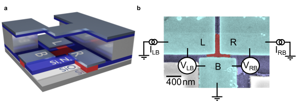
Using the previously introduced technologies of topological insulator selective-area growth and in-situ bridge technology we fabricated three-terminal Josephson junctions, as illustrated in Fig. 1(a) [36, 2]. The geometry of the nanoribbon T-shaped junction for selective-area growth is defined by trenches in a SiO2/Si3N4 (5 nm/15 nm) layer on a highly-resistive Si (111) substrate [37]. First, the 600-nm-wide nanotrenches are etched into the top Si3N4 layer using a combination of electron beam lithography and reactive ion etching. Subsequently, a second set of layers, i.e. a 100-nm-thick SiO2 layer and a 300-nm-thick Si3N4 layer, is deposited on top to define the stencil mask for the in-situ Nb deposition [2]. After patterning the structures for the stencil mask into Si3N4, SiO2 is etched in hydrofluoric acid (HF) forming the free-hanging bridge structures. Simultaneously, the Si(111) surface in the selective-area growth trenches is released in the bottom SiO2 layer defined by the Si3N4 layer on top. The Bi4Te3 layer is selectively grown within these trenches, while the Si3N4 bridge structures are employed to define the geometry of the in situ deposited superconducting electrodes [2]. The Bi4Te3 layer is grown at a temperature of C using molecular beam epitaxy. Subsequently, the 50-nm-thick superconducting Nb electrodes are deposited by electron beam evaporation followed by covering the whole structure with a 5-nm-thick Al2O3 dielectric capping layer. Our processing scheme ensured a high-quality crystalline topological insulator material with clean superconductor interfaces [38, 2], as reported in previous transmission electron microscopy studies. An electron microscopy image of the investigated device is presented in Fig. 1(b).
The measurements of the three-terminal Josephson junction were carried out in a dilution refrigerator with base temperature of . containing a vector magnet. As indicated in Fig. 1(b), the left, right, and bottom junction electrodes are labeled as ”L”, ”R”, and ”B”, respectively. Two current sources supply currents and from L and R to the bottom electrode, respectively, with the according voltages and measured. The differential resistances are measured by adding an ac current of 10 nA to the DC current bias using a lock-in amplifier. The rf-irradiation for the Shapiro step measurements was provided by an antenna placed in close vicinity to the sample.
III Results and Discussion
DC characteristics
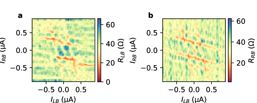
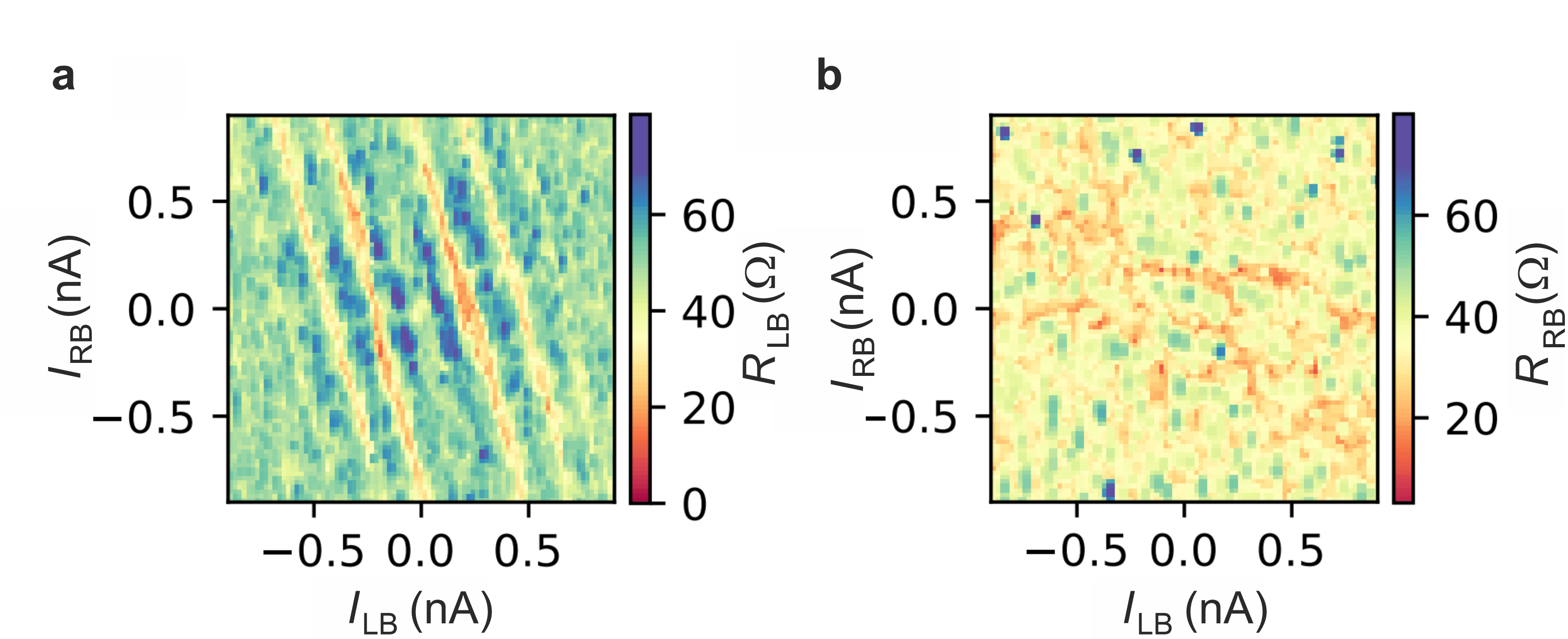
Information about the basic junction characteristics is obtained by measuring the differential resistances and as a function of the bias currents and , respectively. Starting with the left junction we find that shown in Figs 2(a) and (b) contains a superconducting region in the center when and are varied. The observed critical current contour is similar to what has been observed in induced superconducting nano junctions made of high mobility materials such as InAs/Al [3, 24] or graphene [21].
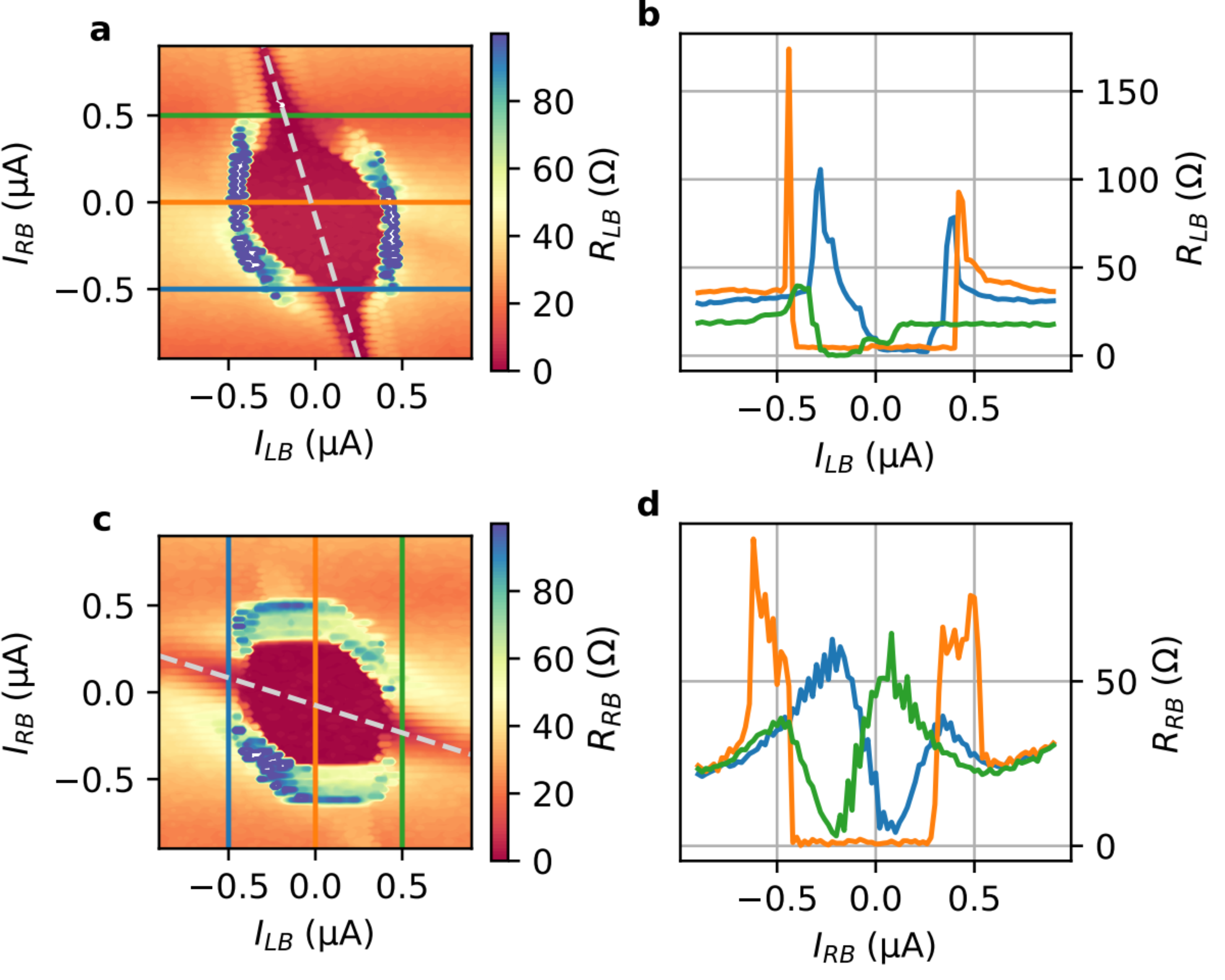
The superconducting region extends along an inclined line indicated by the dashed line in Fig. 2(a). The switching to the superconducting state can be seen in the line cuts at fix values and A provided in Fig. 2(b). The extension of the superconducting state originates from a part of which flows via R to L through the junction between L and B compensating the current partly and by that reducing the total current. For our three-terminal device no reduced differential resistance is observed along the line , which would indicate the presence of a Josephson supercurrent between the junction formed between electrodes L and R [3, 25]. We attribute this to the fact that the distance between these electrodes is slightly larger than for the other junctions so that no Josephson supercurrent is obtained. However, the junction between L and R acts as a shunt resistor taking care that the switching to the superconducting state is non-hysteretic. The differential resistance measured between R and B electrodes, depicted in Figs 2(c) and (d), shows a similar behaviour as , i.e. featuring also an extended superconducting range due a compensation provided by part of . The tilt of the superconducting range indicated by the dashed line in Figure 2(c) is lower compared to Fig. 2(a) since now is the compensating current.
Simulations
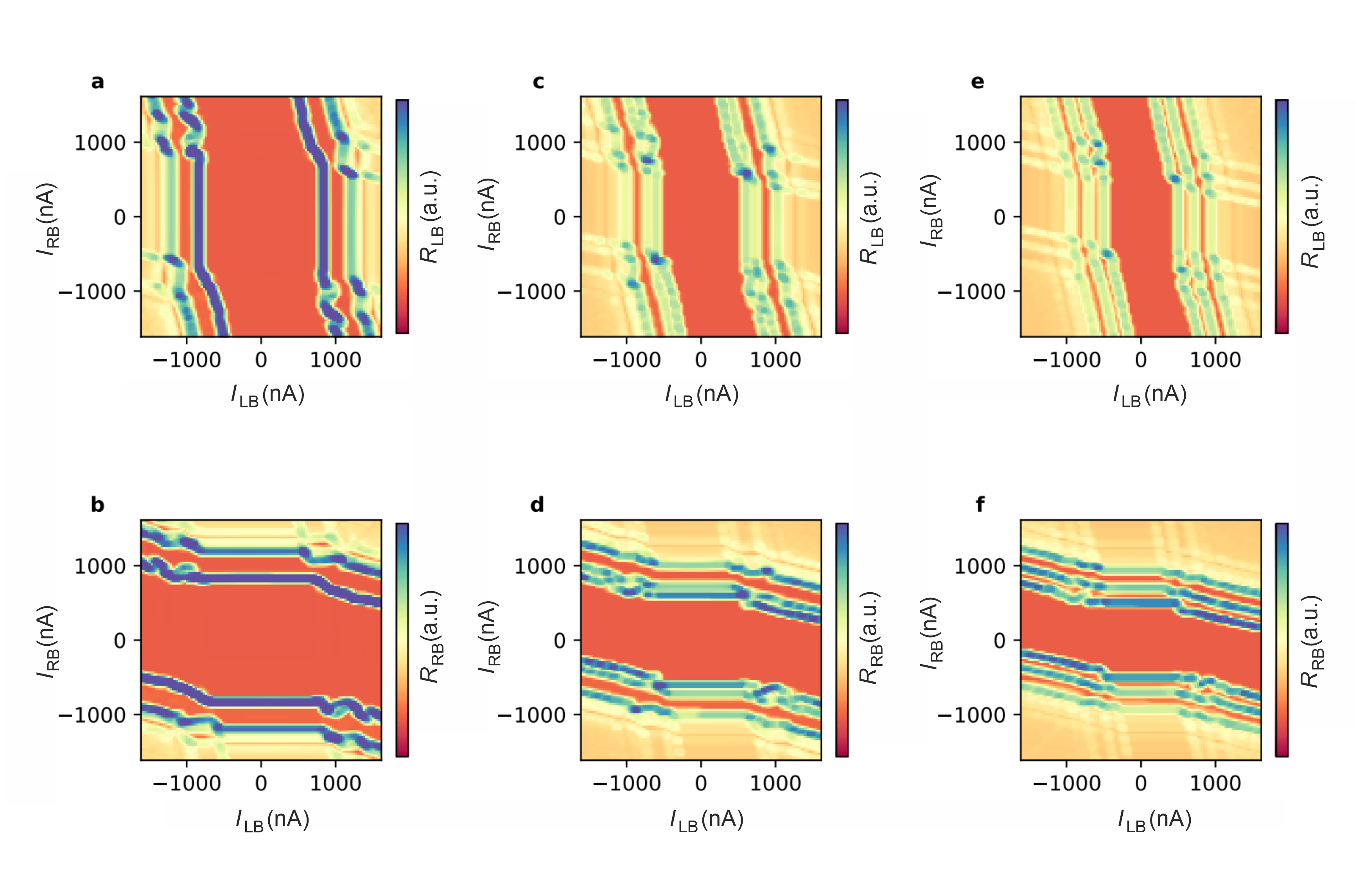
The experimental results are modeled by assuming a network of two resistively and capacitively shunted Josephson (RCSJ) junctions coupled by a resistor , as illustrated in Fig. 3(a). Solving the related system of differential equations numerically, in analogy to what was presented in previous works [3, 4], we simulate the behaviour of the experimental system (information about the procedure see Supplementary Material). The results of the simulations are shown in Figs. 3(b) to (e), where the differential resistance is given as a function of the bias currents and .
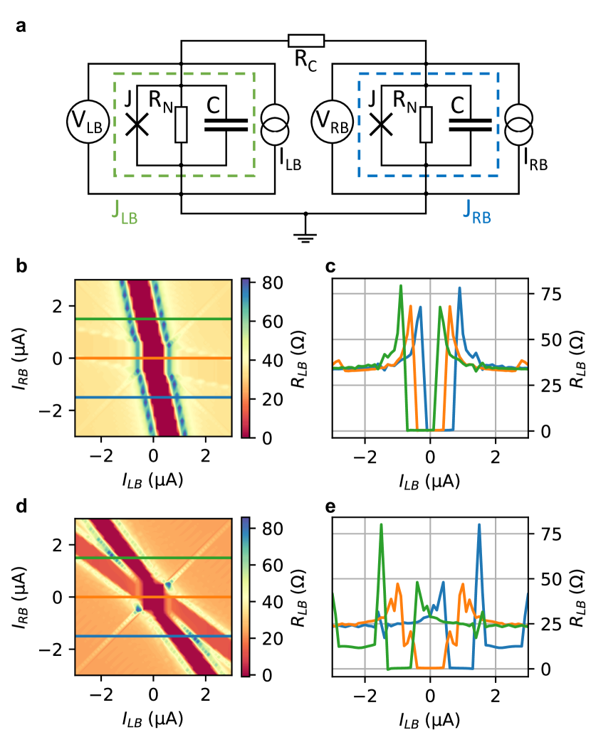
The model describes the experiment well by reproducing the Josephson supercurrent along the inclined lines originating from compensating currents from both electrodes with a superconducting region at the center. The inclination is determined by the coupling resistance . In Figs. 3(b) and (c), the coupling resistance was taken as , with which results in the same tilt as observed experimentally. Taking these values into account the normal state resistance is given by . In our simulations for the critical current and for the Steward-McCumber parameter we assumed and , respectively, with c the junction capacitance. We found that the superconducting state in the junction between R and B leads to some weak feature as a similar line inclined towards horizontal orientation. Note, that for this line is non-zero, as the supercurrent in the other junction only partly reduces the current in the junction between L and B and hence only partially reduces the voltage drop. A noticeable difference between experiment and simulation is that in the measurements the extension of the superconducting state observed along the inclined line (cf. Fig. 2(a) is decreased compared to the simulation depicted in Fig. 3(b). As discussed by Draelos et al. [21], this effect can be explained by dissipation in the neighboring junction being in the normal state resulting in an effective heating, in particular for junctions with small dimensions. In our simulation the direct coupling between the different junctions was neglected. As shown by Arnault et al. [4], including coupling results in a more complex contour of the critical current area. If the coupling resistance becomes very small, i.e. , the observed lines in the differential resistance shift towards the diagonal (cf. Figs. 3(d) and (e). Thus, both junctions are maximally correlated to both current biases and .
Temperature dependence
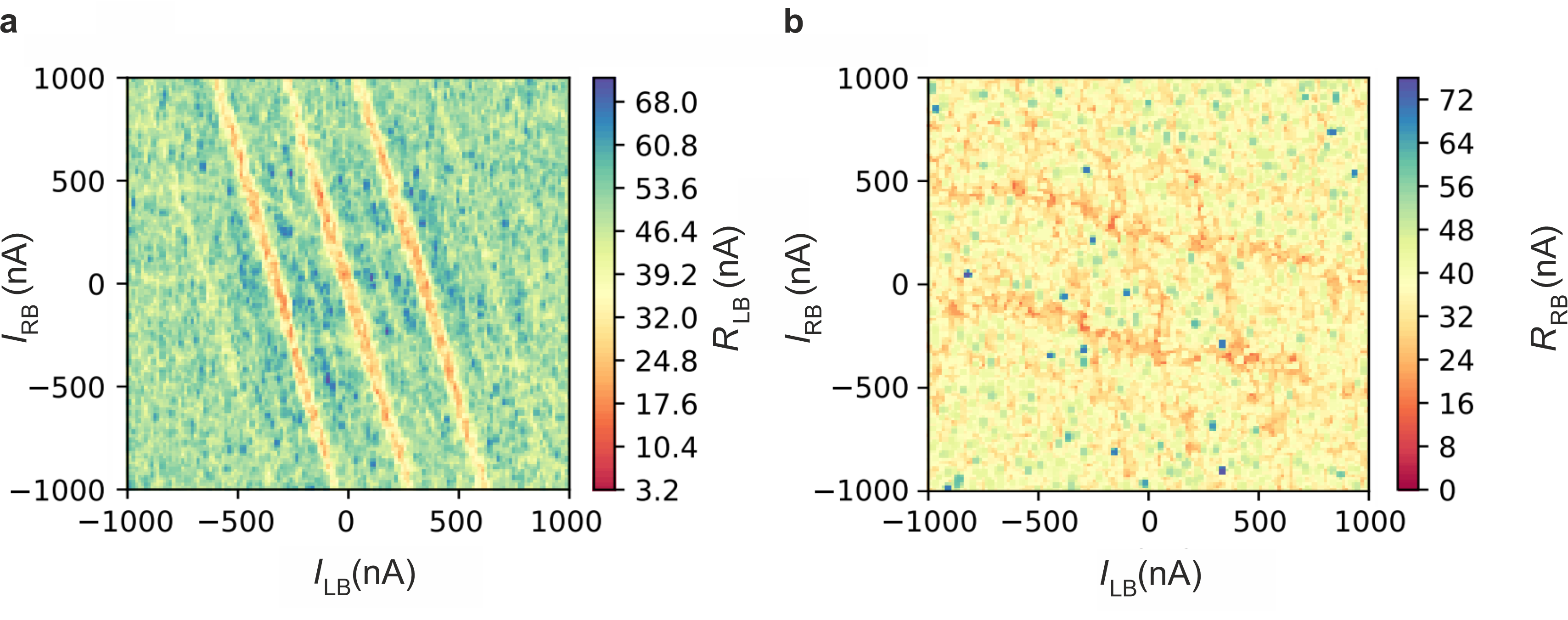
In Figs. 4(a) to (f) the differential resistance maps are shown for and measured at temperatures of 100 mK, 200 mK, and 800 mK.
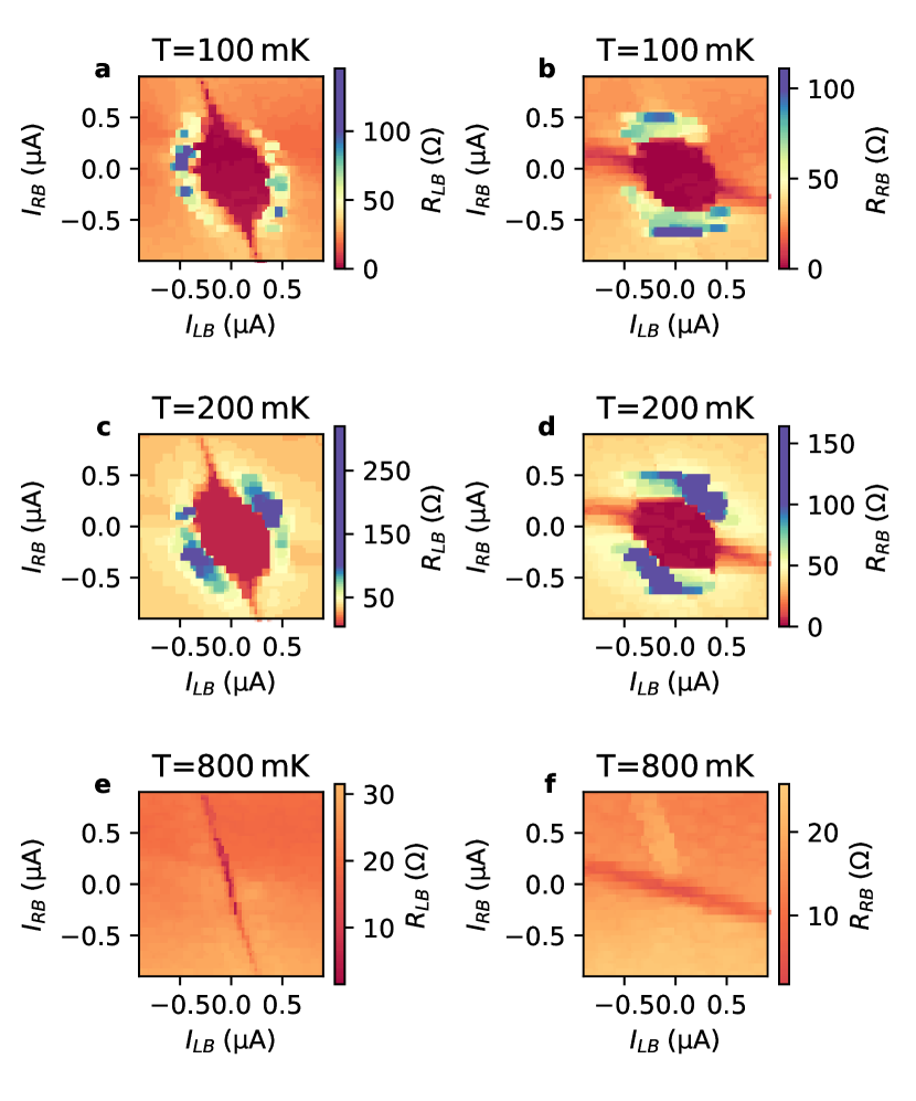
One finds that with increasing temperature the area of the central superconducting region shrinks. This is in accordance with the temperature dependence of the critical current of a single Nb/Bi4Te3/Nb reference junction, as shown in the Supplementary Material. It is noteworthy that the superconducting feature along the inclined lines basically does not change with increasing temperature. This can be explained by the fact, that the dissipation in the neighboring junction already leads to an increased temperature being larger than the substrate temperature.
rf characteristics
Next the radio frequency response of the system is investigated in order to confirm that the experiment is described well by Josephson junction physics and to analyze the rf response of the Josephson current. This is done by first choosing a frequency and an amplitude for the rf irradiation so that both junctions show a large rf response in the differential resistance. Subsequently the same DC bias sweeps are performed as in the prior experiments. Figures 5(a) and (b) show Shapiro step measurements of the differential resistances and , respectively, as a function of bias currents and . The differential resistances are calculated by numerical differentiation. Differential resistances obtained by lock-in amplifier measurements can be found in the Supplementary Material.
The rf frequency and the according power was set to and 0 dBm, respectively. The differential resistances show clear intercrossing stripe-like patterns which can be attributed to the presence of Shapiro steps confirming the presence of a Josephson supercurrent. The intercrossing parallel stripes indicating a coupling of both junctions. By calculating the related voltage drop we find that for both junctions the Shapiro steps are located at integer multiples, , of the characteristic voltage .
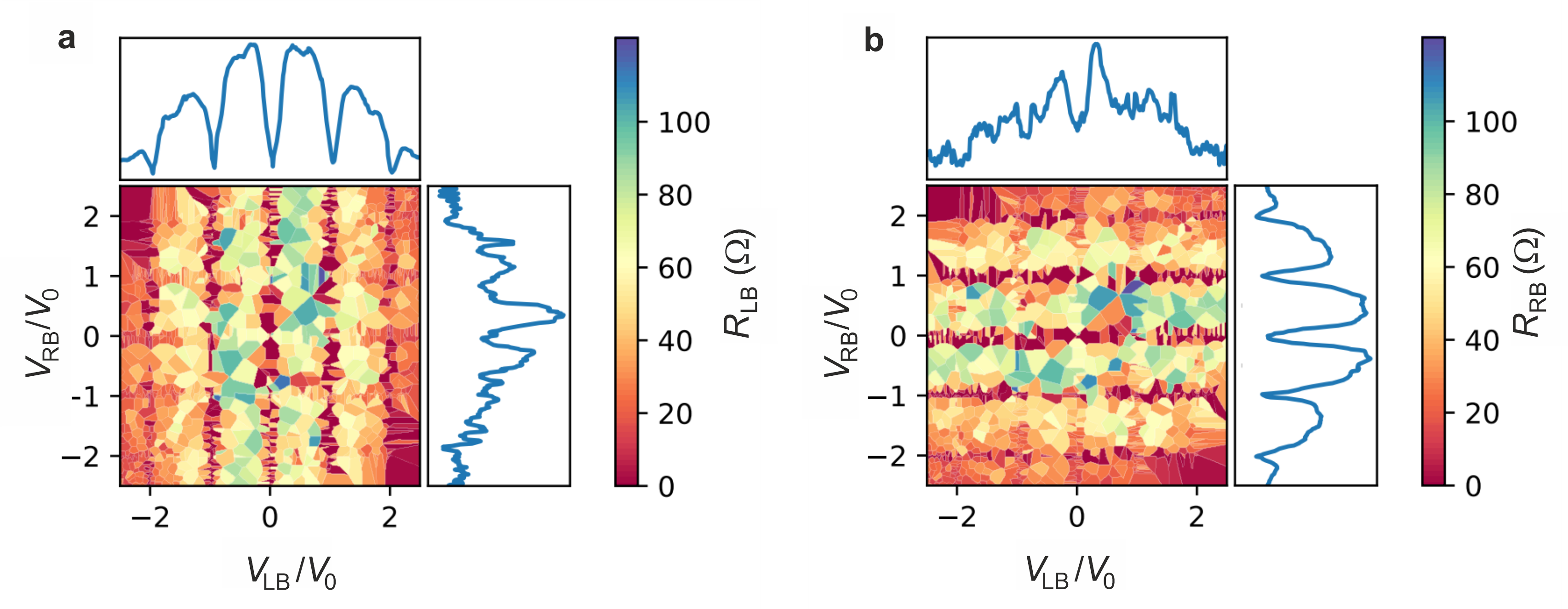
In Figs. 6(a) and (b) the differential resistance maps of and , now taken at at 0 dBm, are depicted, respectively.
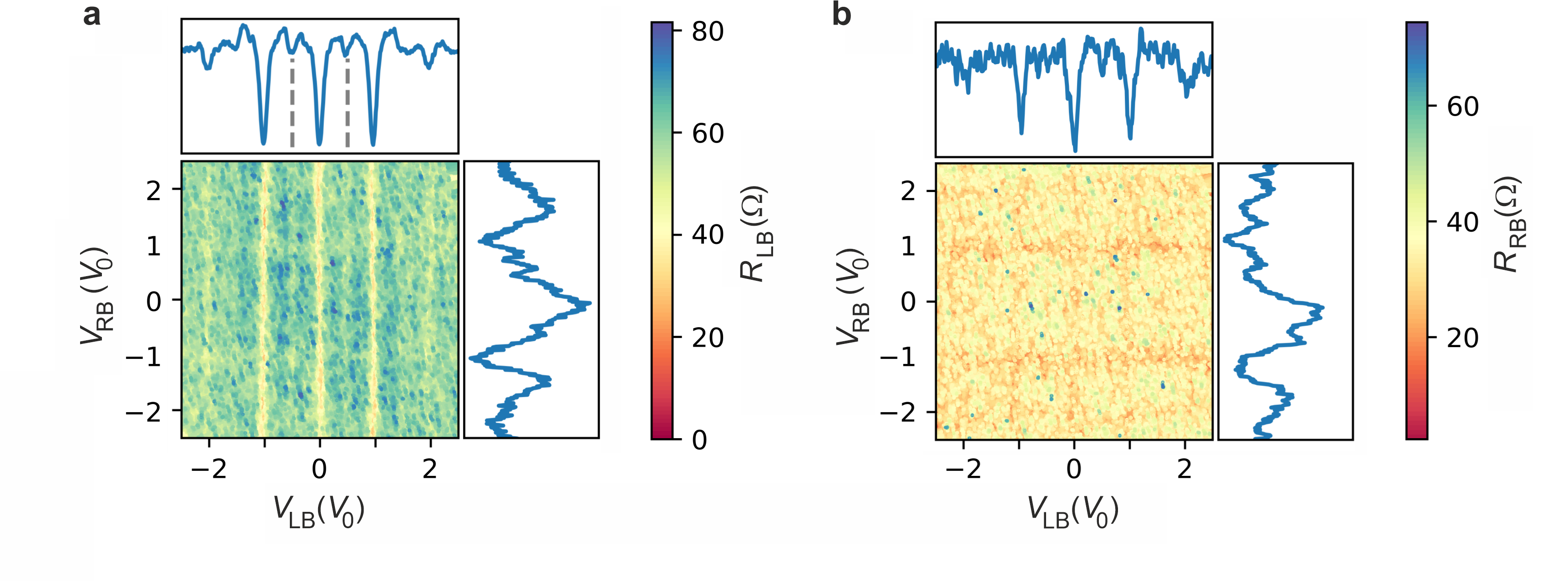
Here, the color maps are plotted as a function of the normalized voltages and . On first sight one finds that the Shapiro step pattern is more pronounced in . We attribute this to a stronger coupling of the rf signal compared to the neighbouring junction due to spatial variations of the rf field. As for the measurements at a coupling of both junctions, although weaker, is observed. Our experimental results of Shapiro step measurements are supported by comparison to simulations based on the previously introduced RCSJ model. In Supplementary Figures 4(a) and (b) maps of the simulated values of and as a function of the normalized bias voltages are shown. There, one finds that the coupling by results in a weak cross coupling of the Shapiro signal resulting in intercrossing stripe-like patterns of different contrast.
A closer inspection of the resistance map presented in Fig. 6(a) reveals that apart from the integer Shapiro steps also half-integer Shapiro steps, e.g. at , are observed. The half integer steps are also clearly resolved in the averaged value of along shown in Fig. 6(a). In single Josephson junctions such fractional steps are interpreted by assuming a skewed current-phase relationship [39, 40, 41] (a simulation for this case using our model is provided in the Supplementary Material). More specifically for multi-terminal junctions the rf response of superconductivity induced into normal metal has been studied previously by Duvauchelle et al. [20]. Here, half-integer steps have been found and interpreted as a feature due to the presence of coherent quartet states. However, in Fig. 2 we did not find indications of quartet states, which would be visible by a feature in the differential resistance at opposite voltage drops on the left and right terminal [18]. Other experimental observations of such fractional steps in multi-terminal junctions are interpreted on the basis of highly connected nonlinear networks of Josephson junctions, where (due to the higher phase space) different transitions of the phase particle in the washboard potential are possible [4]. However, since fractional Shapiro steps were observed in single junctions made with similar materials [42], we favor the explanation based on a skewed current-phase relationship, which can be attributed to contributions of quasi-ballistic transport. In our measurements under rf radiation we did not find indications of missing odd Shapiro steps, as predicted when Majorana bound states are present in topological junctions [43, 2]. Probably, for our samples the narrow width of the Bi4Te3 ribbons prevents the formation of these states, since due to the finite Berry phase a magnetic field along the junctions is required to gain a gap closure for the coherent surface states around the nanoribbon cross section [36].
Magnetic field response
The junction characteristics were also analyzed in a perpendicularly oriented magnetic field . In Fig. 7(a) the magnetic field dependence is plotted as a function of and , while is kept at zero. One clearly observes a Fraunhofer-like interference pattern of the switching current, i.e. the boundary between the red superconducting areas and the areas with finite resistance. The blue line in Fig. 7(a) indicates the according fitting based on the Fraunhofer interference relation. The close resemblance of the experimental data to an ideal Fraunhofer pattern points towards a relatively homogeneous distribution of the supercurrent density. From the fit we extract a period of about , which corresponds to a junction area of . Relating these values to the dimensions of the left junction one finds that the period is about a factor of ten smaller than expected. Based on the actual junction size of a period of is expected for a flux periodicity. We attribute the discrepancy to the experimental period to a pronounced flux focusing effect, where the magnetic field is expelled from the edge regions of the superconducting electrodes and bundled in the junction area. As a matter of fact, a comparably large flux focusing effect was previously observed in similar planar Josephson junctions based on topological insulators and Nb superconducting electrodes [36].
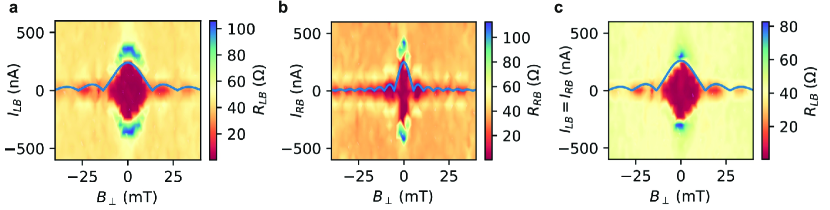
In Fig. 7(b) the magnetic field dependence is shown as a function of and at . Once again, a Fraunhofer-like interference is observed, although with a smaller period, i.e. an larger effective area where the magnetic flux is picked up. The reason for the difference compare to the measurements shown in Fig. 7(a) might be some inhomogeneity in the supercurrent density in the junction. Finally, the maps are scanned diagonally, i.e. , as shown in Fig. 7(c). Here, once again a regular Fraunhofer pattern is observed, which is almost identical to the pattern shown in Fig. 7(d), indication, that the current through the neighboring junction basically has not effect.
IV Conclusion
We have succeeded in extending the previously developed in situ fabrication technology for Josephson junctions to a working more complex design of a three-terminal junction. Analysis of the transport experiments shows that our system indeed behaves like a coupled network of Josephson junctions in DC transport, rf response, as well as magnetic field response. This is the first report on the topological multi-terminal devices where an interaction between the individual Josephson junctions is observed. Moreover, the observation of fractional steps in the rf response opens a window that provides a first insight into the novel physics of this type of device. On a more technical level, our results demonstrate the realization of more complex devices required for network structures in topological quantum circuits.
Further investigations and detailed understanding of such a system are crucial for the realization of complex topological quantum systems. In future, similar experiments with more intricate circuit designs and superconducting phase controlled measurements will be performed. The complexities in the junction characteristics arose from the selected weak-link material Bi4Te3. In future experiments we plan to incorporate conventional three-dimensional topological insulators, e.g. Bi2Te3, Sb2Te3, Bi2Se3, and the topological Dirac semimetal exhibited by the correctly tuned BixTey stoichiometric alloy.
Acknowledgement
We thank Herbert Kertz for technical assistance as well as Kristof Moors and Roman Riwar for fruitful discussion. This work was partly funded by the Deutsche Forschungsgemeinschaft (DFG, German Research Foundation) under Germany’s Excellence Strategy—Cluster of Excellence Matter and Light for Quantum Computing (ML4Q) EXC 2004/1—390534769, the German Federal Ministry of Education and Research (BMBF) via the Quantum Futur project “MajoranaChips” (Grant No. 13N15264) within the funding program Photonic Research Germany, as well as the Bavarian Ministry of Economic Affairs, Regional Development and Energy within Bavaria’s High-Tech Agenda Project “Bausteine für das Quantencomputing auf Basis topologischer Materialien mit experimentellen und theoretischen Ansätzen“ (grant allocation no. 07 02/686 58/1/21 1/22 2/23).
References
- Kitaev [2003] A. Kitaev, Fault-tolerant quantum computation by anyons, Annals of Physics 303, 2 (2003).
- Hyart et al. [2013] T. Hyart, B. van Heck, I. C. Fulga, M. Burrello, A. R. Akhmerov, and C. W. J. Beenakker, Flux-controlled quantum computation with Majorana fermions, Phys. Rev. B 88, 035121 (2013).
- Aasen et al. [2016] D. Aasen, M. Hell, R. V. Mishmash, A. Higginbotham, J. Danon, M. Leijnse, T. S. Jespersen, J. A. Folk, C. M. Marcus, K. Flensberg, and J. Alicea, Milestones toward Majorana-based quantum computing, Phys. Rev. X 6, 031016 (2016).
- Manousakis et al. [2017] J. Manousakis, A. Altland, D. Bagrets, R. Egger, and Y. Ando, Majorana qubits in a topological insulator nanoribbon architecture, Phys. Rev. B 95, 165424 (2017).
- Cook and Franz [2011] A. Cook and M. Franz, Majorana fermions in a topological-insulator nanowire proximity-coupled to an -wave superconductor, Phys. Rev. B 84, 201105 (2011).
- Cook et al. [2012] A. M. Cook, M. M. Vazifeh, and M. Franz, Stability of Majorana fermions in proximity-coupled topological insulator nanowires, Phys. Rev. B 86, 155431 (2012).
- Legg et al. [2021] H. F. Legg, D. Loss, and J. Klinovaja, Majorana bound states in topological insulators without a vortex, Phys. Rev. B 104, 165405 (2021).
- Fu and Kane [2008] L. Fu and C. L. Kane, Superconducting proximity effect and Majorana fermions at the surface of a topological insulator, Phys. Rev. Lett. 100, 096407 (2008).
- Stenger et al. [2019] J. P. T. Stenger, M. Hatridge, S. M. Frolov, and D. Pekker, Braiding quantum circuit based on the Josephson effect, Phys. Rev. B 99, 035307 (2019).
- Yokoyama and Nazarov [2015] T. Yokoyama and Y. V. Nazarov, Singularities in the Andreev spectrum of a multiterminal Josephson junction, Phys. Rev. B 92, 155437 (2015).
- Eriksson et al. [2017] E. Eriksson, R.-P. Riwar, M. Houzet, J. S. Meyer, and Y. V. Nazarov, Topological transconductance quantization in a four-terminal Josephson junction, Phys. Rev. B 95, 075417 (2017).
- Xie et al. [2018] H.-Y. Xie, M. G. Vavilov, and A. Levchenko, Weyl nodes in Andreev spectra of multiterminal Josephson junctions: Chern numbers, conductances, and supercurrents, Phys. Rev. B 97, 035443 (2018).
- Riwar et al. [2016] R.-P. Riwar, M. Houzet, J. S. Meyer, and Y. V. Nazarov, Multi-terminal Josephson junctions as topological matter, Nature Comm. 7, 1 (2016).
- Houzet and Samuelsson [2010] M. Houzet and P. Samuelsson, Multiple Andreev reflections in hybrid multiterminal junctions, Phys. Rev. B 82, 060517 (2010).
- Freyn et al. [2011] A. Freyn, B. Douçot, D. Feinberg, and R. Mélin, Production of nonlocal quartets and phase-sensitive entanglement in a superconducting beam splitter, Phys. Rev. Lett. 106, 257005 (2011).
- Nowak et al. [2019] M. P. Nowak, M. Wimmer, and A. R. Akhmerov, Supercurrent carried by nonequilibrium quasiparticles in a multiterminal Josephson junction, Phys. Rev. B 99, 075416 (2019).
- Melo et al. [2022] A. Melo, V. Fatemi, and A. R. Akhmerov, Multiplet supercurrent in Josephson tunneling circuits, SciPost Phys. 12, 17 (2022).
- Pfeffer et al. [2014] A. H. Pfeffer, J. E. Duvauchelle, H. Courtois, R. Mélin, D. Feinberg, and F. Lefloch, Subgap structure in the conductance of a three-terminal Josephson junction, Phys. Rev. B 90, 075401 (2014).
- Cohen et al. [2018] Y. Cohen, Y. Ronen, J.-H. Kang, M. Heiblum, D. Feinberg, R. Mélin, and H. Shtrikman, Nonlocal supercurrent of quartets in a three-terminal Josephson junction, Proceedings of the National Academy of Sciences 115, 6991 (2018).
- Duvauchelle et al. [2016] J. E. Duvauchelle, A. H. Pfeffer, H. Courtois, and F. Lefloch, Quantum coherence of the quartet scheme observed by Shapiro resonance under radio-frequency irradiation in three terminal Josephson junctions, IEEE Transactions on Applied Superconductivity 26, 1 (2016).
- Draelos et al. [2019] A. W. Draelos, M.-T. Wei, A. Seredinski, H. Li, Y. Mehta, K. Watanabe, T. Taniguchi, I. V. Borzenets, F. Amet, and G. Finkelstein, Supercurrent flow in multiterminal graphene Josephson junctions, Nano Letters 19, 1039–1043 (2019).
- Arnault et al. [2021] E. G. Arnault, T. F. Q. Larson, A. Seredinski, L. Zhao, S. Idris, A. McConnell, K. Watanabe, T. Taniguchi, I. Borzenets, F. Amet, and G. Finkelstein, Multiterminal inverse ac Josephson effect, Nano Letters 21, 9668 (2021).
- Graziano et al. [2020] G. V. Graziano, J. S. Lee, M. Pendharkar, C. J. Palmstrøm, and V. S. Pribiag, Transport studies in a gate-tunable three-terminal Josephson junction, Phys. Rev. B 101, 054510 (2020).
- Pankratova et al. [2020] N. Pankratova, H. Lee, R. Kuzmin, K. Wickramasinghe, W. Mayer, J. Yuan, M. G. Vavilov, J. Shabani, and V. E. Manucharyan, Multiterminal Josephson effect, Phys. Rev. X 10, 031051 (2020).
- Graziano et al. [2022] G. V. Graziano, M. Gupta, M. Pendharkar, J. T. Dong, C. P. Dempsey, C. Palmstrøm, and V. S. Pribiag, Selective control of conductance modes in multi-terminal Josephson junctions, arXiv preprint arXiv:2201.01373 (2022).
- Kurter et al. [2015] C. Kurter, A. Finck, Y. S. Hor, and D. J. Van Harlingen, Evidence for an anomalous current–phase relation in topological insulator Josephson junctions, Nature Comm. 6, 1 (2015).
- Yang et al. [2019] G. Yang, Z. Lyu, J. Wang, J. Ying, X. Zhang, J. Shen, G. Liu, J. Fan, Z. Ji, X. Jing, F. Qu, and L. Lu, Protected gap closing in Josephson trijunctions constructed on Bi2Te3 , Phys. Rev. B 100, 180501 (2019).
- Schüffelgen et al. [2019] P. Schüffelgen, D. Rosenbach, C. Li, T. W. Schmitt, M. Schleenvoigt, A. R. Jalil, S. Schmitt, J. Kölzer, M. Wang, B. Bennemann, U. Parlak, L. Kibkalo, S. Trellenkamp, T. Grap, D. Meertens, M. Luysberg, G. Mussler, E. Berenschot, N. Tas, A. A. Golubov, A. Brinkman, T. Schäpers, and D. Grützmacher, Selective area growth and stencil lithography for in situ fabricated quantum devices, Nature Nanotechnology 14, 825 (2019).
- Saito et al. [2017] Y. Saito, P. Fons, K. Makino, K. V. Mitrofanov, F. Uesugi, M. Takeguchi, A. V. Kolobov, and J. Tominaga, Compositional tuning in sputter-grown highly-oriented Bi–Te films and their optical and electronic structures, Nanoscale 9, 15115 (2017).
- Chagas et al. [2020] T. Chagas, G. A. S. Ribeiro, P. H. R. Gonçalves, L. Calil, W. S. Silva, Â. Malachias, M. S. C. Mazzoni, and R. Magalhães-Paniago, Bi2:Bi2Te3 stacking influence on the surface electronic response of the topological insulator Bi4Te3, Electronic Structure 2, 015002 (2020).
- Chagas et al. [2022] T. Chagas, O. A. Ashour, G. A. S. Ribeiro, W. S. Silva, Z. Li, S. G. Louie, R. Magalhães Paniago, and Y. Petroff, Multiple strong topological gaps and hexagonal warping in Bi4Te3, Phys. Rev. B 105, L081409 (2022).
- Nabok et al. [2022] D. Nabok, M. Tas, S. Kusaka, E. Durgun, C. Friedrich, G. Bihlmayer, S. Blügel, T. Hirahara, and I. Aguilera, Bulk and surface electronic structure of Bi4Te3 from GW calculations and photoemission experiments, Phys. Rev. Materials 6, 034204 (2022).
- Jalil [2022] A. R. Jalil, Engineering topological superlattices and their epitaxial integration in selectively grown hybrid nanostructures via MBE, Ph.D. thesis, RWTH Aachen University (2022).
- Yang and Nagaosa [2014] B.-J. Yang and N. Nagaosa, Classification of stable three-dimensional dirac semimetals with nontrivial topology, Nature Comm. 5, 1 (2014).
- Rauch et al. [2014] T. c. v. Rauch, M. Flieger, J. Henk, I. Mertig, and A. Ernst, Dual topological character of chalcogenides: Theory for Bi2Te3, Phys. Rev. Lett. 112, 016802 (2014).
- Rosenbach et al. [2021] D. Rosenbach, T. W. Schmitt, P. Schüffelgen, M. P. Stehno, C. Li, M. Schleenvoigt, A. R. Jalil, G. Mussler, E. Neumann, S. Trellenkamp, A. A. Golubov, A. Brinkman, D. Grützmacher, and T. Schäpers, Reappearance of first Shapiro step in narrow topological Josephson junctions, Science Advances 7, eabf1854 (2021).
- Schmitt et al. [2022] T. W. Schmitt, M. R. Connolly, M. Schleenvoigt, C. Liu, O. Kennedy, J. M. Chávez-Garcia, A. R. Jalil, B. Bennemann, S. Trellenkamp, F. Lentz, et al., Integration of topological insulator Josephson junctions in superconducting qubit circuits, Nano Letters 22, 2595 (2022).
- Kölzer et al. [2021] J. Kölzer, K. Moors, A. R. Jalil, E. Zimmermann, D. Rosenbach, L. Kibkalo, P. Schüffelgen, G. Mussler, D. Grützmacher, T. L. Schmidt, H. Lüth, and T. Schäpers, In-plane magnetic field-driven symmetry breaking in topological insulator-based three-terminal junctions, Comm. Materials 2, 116 (2021).
- Snyder et al. [2018] R. A. Snyder, C. J. Trimble, C. C. Rong, P. A. Folkes, P. J. Taylor, and J. R. Williams, Weak-link Josephson junctions made from topological crystalline insulators, Phys. Rev. Lett. 121, 097701 (2018).
- Panghotra et al. [2020] R. Panghotra, B. Raes, C. C. de Souza Silva, I. Cools, W. Keijers, J. E. Scheerder, V. V. Moshchalkov, and J. Van de Vondel, Giant fractional Shapiro steps in anisotropic Josephson junction arrays, Comm. Physics 3, 53 (2020).
- Raes et al. [2020] B. Raes, N. Tubsrinuan, R. Sreedhar, D. S. Guala, R. Panghotra, H. Dausy, C. C. de Souza Silva, and J. Van de Vondel, Fractional Shapiro steps in resistively shunted Josephson junctions as a fingerprint of a skewed current-phase relationship, Phys. Rev. B 102, 054507 (2020).
- Rosenbach [2021] D. Rosenbach, Quantum transport and induced superconductivity in selectively deposited topological insulator devices, Dissertation, RWTH Aachen University, Aachen (2021).
- Domínguez et al. [2017] F. Domínguez, O. Kashuba, E. Bocquillon, J. Wiedenmann, R. S. Deacon, T. M. Klapwijk, G. Platero, L. W. Molenkamp, B. Trauzettel, and E. M. Hankiewicz, Josephson junction dynamics in the presence of - and -periodic supercurrents, Phys. Rev. B 95, 195430 (2017).
Supplementary Material: Supercurrent in Bi4Te3 Topological Material-Based Three-Terminal Junctions
SI Single junction measurements
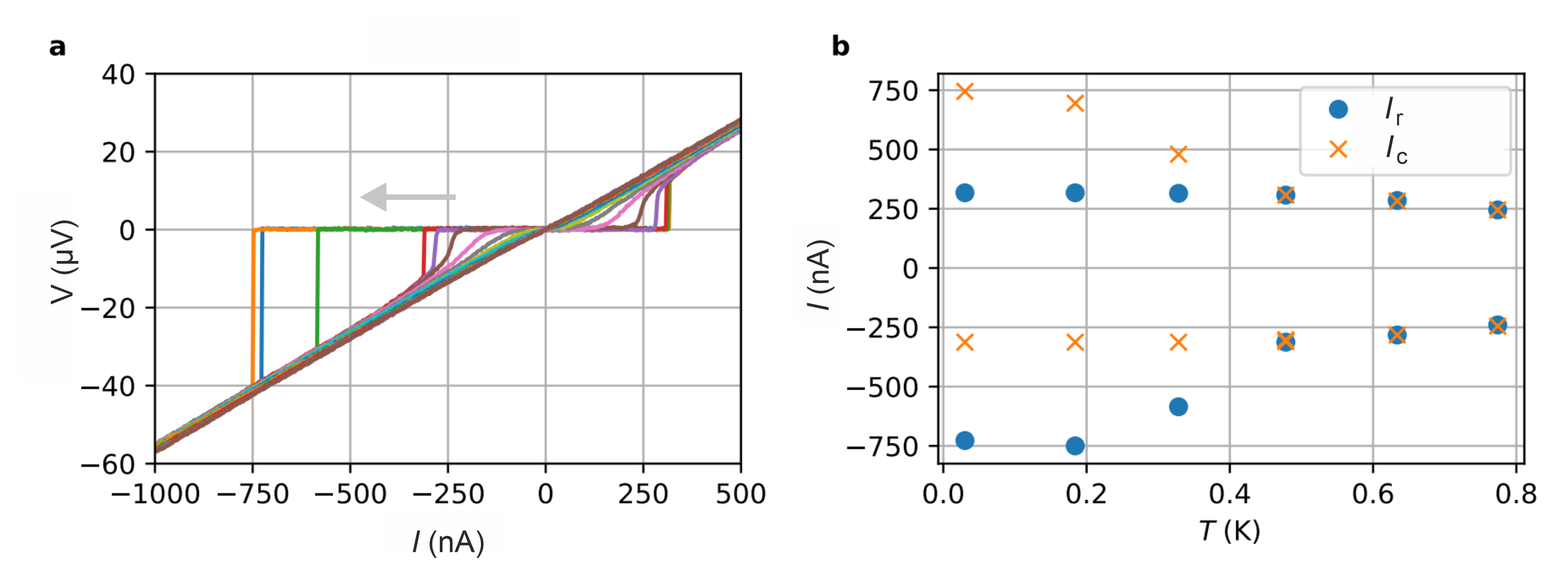
As a reference a single Nb/Bi4Te3/Nb junction was measured. The junction has a length of and a width of . In Supplementary Figure S1(a) the current voltage characteristics is shown at temperatures in the range from to . At lowest temperature a critical current of is obtained. In contrast to the three terminal junction, here, a hysteretic behaviour is observed, which can be explained by the missing shunt for the single Josephson junction. We attribute the hysteresis to heating resulting in a lower return current compared to [1]. The critical current monotonously decreases with temperature with some kink around . The latter might be attributed to a switching from a more diffusive to a more ballistic transport in the weak link [2].
SII RCSJ model for a three-terminal junction
The characteristics of our three-terminal junctions is simulated by employing a two-dimensional resistively and capacitively shunted Josephson junction (RCSJ) Ansatz in analogy to what was presented in previous works [3, 4]. In Fig. 3(a) in the main text the corresponding network is depicted including two resistively and capacitively shunted Josephson junctions with the normal state resistance and the capacitance . We assume two identical junctions each having a critical current of . The junctions are connected by a coupling resistor representing the non-superconducting junction between electrodes L and R. Following the RCSJ Ansatz the characteristics of the three-terminal junction can be described by a set of coupled differential equations of the form:
| (S1) |
| (S2) |
with and the phase differences between junctions and , respectively, the normalized time, , with the magnetic flux quantum, and the Stewart-McCumber parameter [5]. The equations are similar to the standard RCSJ model for a single junction, except of the last term, which introduces the current through the resistor, coupling the two junctions. This current is a result of the voltage difference between the two junctions and the coupling resistance. For the coupling term goes to zero, leading to two individual junctions (decoupled system) and for the system is dominated by the coupling term.
SIII Shapiro Steps in Three-Terminal Junction Experiments
The differential resistances and exposed to an rf radiation with a frequency of at 0 dBm recorded as a function of the applied DC currents are presented in Supplementary Figures S2(a) and (b). In contrast to the corresponding figure, which was gained by numerical differentiation, here, the resistance is directly taken using a lock-in amplifier. In Supplementary Figures S3 the corresponding measurements at a frequency of at 0 dBm are shown.
SIV Shapiro Steps in Three-Terminal Junction Simulation
Using the model described in Supplementary Information SII the Shapiro response was simulated by adding an oscillation contribution , , to the dc bias currents. The simulated differential resistances and as a function of the normalized voltage drops at a frequency of are presented in Supplementary Figures S4(a) and (b). One finds that the Shapiro response is strong in the corresponding junctions, while the coupling from the neighboring junction is weak.
In order to simulate the appearance of the fractional Shapiro steps a non-sinusoidal current-phase relationship was assumed for the Josephson junction by including a contribution. In Supplementary Figures S5(a) and (b) the respective simulation outcomes and for junctions and are shown as a function of bias currents. One finds that by increasing the contribution fractional steps appear.
References
- Courtois et al. [2008] H. Courtois, M. Meschke, J. T. Peltonen, and J. P. Pekola, Origin of hysteresis in a proximity Josephson junction, Physical Review Letters 101, 067002 (2008).
- Schüffelgen et al. [2019] P. Schüffelgen, D. Rosenbach, C. Li, T. W. Schmitt, M. Schleenvoigt, A. R. Jalil, S. Schmitt, J. Kölzer, M. Wang, B. Bennemann, U. Parlak, L. Kibkalo, S. Trellenkamp, T. Grap, D. Meertens, M. Luysberg, G. Mussler, E. Berenschot, N. Tas, A. A. Golubov, A. Brinkman, T. Schäpers, and D. Grützmacher, Selective area growth and stencil lithography for in situ fabricated quantum devices, Nature Nanotechnology 14, 825 (2019).
- Graziano et al. [2020] G. V. Graziano, J. S. Lee, M. Pendharkar, C. J. Palmstrøm, and V. S. Pribiag, Transport studies in a gate-tunable three-terminal Josephson junction, Phys. Rev. B 101, 054510 (2020).
- Arnault et al. [2021] E. G. Arnault, T. F. Q. Larson, A. Seredinski, L. Zhao, S. Idris, A. McConnell, K. Watanabe, T. Taniguchi, I. Borzenets, F. Amet, and G. Finkelstein, Multiterminal inverse ac Josephson effect, Nano Letters 21, 9668 (2021).
- Tinkham [2004] M. Tinkham, Introduction to Superconductivity (Dover Publications, New York, 2004).