Mechanical scanning probe lithography of perovskites for fabrication of high-Q planar polaritonic cavities
Abstract
Exciton-polaritons are unique quasiparticles with hybrid properties of an exciton and a photon, opening ways to realize ultrafast strongly nonlinear systems and inversion-free lasers based on Bose-Einstein polariton condensation. However, the real-world applications of the polariton systems are still limited due to the temperature operation and costly fabrication techniques for both exciton materials and photon cavities. 2D perovskites represent one of the most prospective platforms for the realization of strong light-matter coupling since they support room-temperature exciton states with large oscillator strength and can simultaneously be used for the fabrication of planar photon cavities with high field localization due to the high refractive index of the material. In this work, we demonstrate the affordable for research purposes mechanical scanning probe lithography method for the realization of room-temperature exciton-polariton systems based on the 2D perovskite (PEA)2PbI4 with the Rabi splitting exceeding 200 meV. By the precise control of the lithography parameters, we broadly adjust the exciton-polariton dispersion and, in particular, vary the radiative coupling of polaritonic modes to the free space. Our findings represent a versatile approach to the fabrication of planar high-quality perovskite-based photonic cavities supporting the strong light-matter coupling regime for the development of on-chip all-optical active and nonlinear polaritonic devices.
Photonics deals both with fundamental and applied aspects of operating with optical signals, as well as with prospective designing energy-efficient optical computing devices. Implementing such devices where light is controlled by light requires systems with strong optical nonlinearity. Optical systems with the strong coupling of photon cavity mode with an exciton resonance, resulting in exciton-polariton, demonstrate a nonlinear response up to 3-4 orders of magnitude higher than in weakly coupled systems.Bélanger, Villeneuve, and Aitchison (1997) Such systems are realized by embedding an excitonic material with high exciton oscillator strength into a photon cavity supporting a mode with strong field enhancement and a long radiative lifetime. Kavokin et al. (2017) The search for excitonic materials as well as the design of photon cavities suitable for the incorporation with efficient fabrication methods is therefore of great importance for polaritonics today.
One of the most studied and widely used material platforms for the exciton-polariton systems is the GaAs quantum well (QW), embedded into the vertical Bragg cavity.Weisbuch et al. (1992) Due to the low exciton binding energy, the operation of these polariton systems is limited to cryogenic temperatures.Bajoni et al. (2008); Kasprzak et al. (2006) The temperature limitations can be overcome with wide-gap semiconductor QWs such as ZnOvan Vugt et al. (2006) or GaN Semond et al. (2005), but they still require time-consuming and costly fabrication methods such as epitaxial growth techniques. Monolayer transition metal dichalcogenides have become perspective materials for room-temperature polariton systems, Stepanov et al. (2021); Kravtsov et al. (2020) though their potential applications are still limited by technological scalability. Currently, halide perovskites represent the promising platform for exciton-polariton systems due to their easy and cost-efficient fabrication as well as their outstanding excitonic properties making it possible to implement room-temperature exciton-polariton systems.Su et al. (2021) Moreover, two-dimensional perovskites with enormous exciton binding energy in the range of meVGélvez-Rueda et al. (2020) and exceptionally strong excitonic response Zhao et al. (2018) have experimentally demonstrated the record-high value of Rabi splitting among perovskites exceeding 200 meV at room temperature Wang et al. (2018) and therefore represent one of the promising materials for polaritonic systems.
The most commonly used photon resonator in polaritonic systems is the vertical Bragg cavity since it provides all necessary requirements such as low optical losses, controllable lifetimes, and high field enhancement.Butté et al. (2005) Exciton-polaritons in perovskite materials and also in 2D-perovskites have been already demonstrated in the Bragg resonators.Wang et al. (2018); Su et al. (2020); Wu et al. (2021) Nevertheless, such structures are bulky, i.e. have large vertical sizes and also require sophisticated and costly fabrication methods, which severely hinder real-world applications.Sturm et al. (2009) Meanwhile, compatible with on-chip designs planar photon cavities, such as metasurfaces or photonic crystal slabs (PCSs) can demonstrate comparable characteristics and have been recently employed in exciton-polariton systems with various materials.Whittaker et al. (2021); Kravtsov et al. (2020); Masharin et al. (2022a) Moreover, high-Q symmetry-protected bound states in the continuum (BICs), appearing in metasurfaces, when strongly coupled to the exciton resonance,Koshelev et al. (2018) allow to even realize polariton Bose–Einstein condensation.Ardizzone et al. (2022) Although planar photon cavities based on perovskites are more suitable for future applications, there is still a lack of efficient and low-cost cavity fabrication techniques.
Previously, several methods for perovskite nanostructuring have already been demonstrated, however, all of them have disadvantages and limitations. The material degradation may be caused during focused ion beam and electron beam lithography Alias et al. (2015); Lamers, Zhang, and Wallentin (2022). Direct laser writing avoids this problem but has a limited lateral resolution above 200 nm.Zhizhchenko et al. (2021) Nanoimprint method maintains the resolution of ion (or electron) beam lithography and does not cause degradation, but the stamp geometry can not be changed after its fabrication.Masharin et al. (2022a, b) From this point of view, mechanical scanning probe lithography (m-SPL)Garcia, Knoll, and Riedo (2014) (Fig. 1a) appears one of the most versatile and convenient nanostructuring techniques for the perovskite planar exciton-polariton system since the mechanical cutting of perovskites does not cause material degradation, the atomic force microscopy (AFM) tip can be less than 10 nm in its lateral sizes, and high-precision piezo-stages of m-SPL allow for the dynamic tuning of various parameters of the resulting structure.
In this work, we demonstrate a universal and affordable for research purposes technology of 2D-perovskite film nanostructuring for the realization of room-temperature exciton-polariton planar cavities based on PCS with the precise control of polariton dispersion. By varying the period and modulation of PCS we change the exciton-polariton dispersion and its radiative lifetime. The developed m-SPL method for perovskites opens the way for the realization of planar polaritonic cavities with on-demand optical properties for nonlinear and active polaritonics.
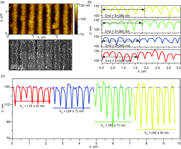
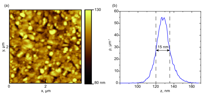
To fabricate the sample, first, a thin film of 2D perovskite is synthesized by the solvent engineering methodJeon et al. (2014). The solution for the synthesis is prepared by dissolving 149.4 mg of PEAI and 138.3 mg of PbI2 in 1 ml of dimethylformamide. Before the synthesis of the thin film, we clean 1212 mm SiO2 substrates with soapy water, acetone, and isopropanol consistently. To achieve the hydrophilic surface of the substrates, they are placed in the oxygen plasma cleaner for 10 minutes. The synthesis of (PEA)2PbI4 films is performed in a glove box with a dry nitrogen atmosphere with the spin-coating method. The prepared perovskite solution is deposited on top of the substrate and after it accelerates for 2 seconds and rotates at a speed of 4000 rpm for 60 seconds. The resulting film is annealed at 70∘ for 10 minutes. The morphology of the synthesized film is studied with AFM, resulting in 130 nm film thickness and surface roughness of 15 nm (See Fig. S1 in Supplementary Information (SI)).
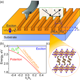
For m-SPL we use an atomic force microscope AIST-NT SMART SPM and cantilevers with a single-crystal diamond tip (TipsNano DRP-IN) with a resonant frequency of 500 – 1000 kHz, a normal spring constant of 350 N/m (See SI for the details), and a tip curvature radius of 25 – 35 nm. Before the lithography, the film morphology was characterized with AFM in a semi-contact regime. The use of the piezo-stages of the atomic force microscope makes it possible to control the diamond-tipped cantilever position with an accuracy of nanometers. Thus, fabricating the 1D PCS, we precisely control the period, the height modulation, and the trench width (see Fig.1a).
During the fabrication, the cantilever is pushed towards the surface with force controlled by the AFM feedback system. The cantilever moves once along the specified direction, forming trenches in the perovskite film. During trench formation, the material is partially compressed and partially ejected towards the sides of the trench. However, most of it is moved by the tip to the end of the trench. At the end of each trench, the probe lifts off the film surface. The cut grains remain at the edge of the fabricated structure and do not affect the optical properties of the whole PCS.
The height modulation depends on the applied cantilever force, which is defined by the shift of the cantilever from the initial position and its stiffness. The force required to achieve a modulation of nm on perovskite films is experimentally estimated to be in the range of . Since the tip is conical in shape, the minimum trench width depends on the modulation . For modulation of nm, the width at the half-height of the trench is nm (See SI for more details). The speed of the cantilever during the lithography process is limited by 3 /s because at higher values the probe begins to pull out perovskite grains. The optimal speed for the 2D-perovskite film lithography is found to be approximately 1 /s.
By choosing the trajectory of the AFM tip with piezo-stages, this method allows the realization of mostly arbitrary structures. Particularly, it is possible to change the period of the PCS by programming the cantilever movement coordinates with nanometer precision. One of the most important advantages of m-SPL is the potential applicability of this method for the creation of PCSs, coupled waveguides, or other planar photonic designs on one 2D-perovskite film, combining them into one photonic on-chip system.
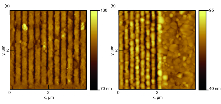
The fabricated PCSs have a lateral size of 15x30 . The typical morphology of the structure studied with AFM and scanning electron microscopy (SEM) is shown in Fig. 2a. By varying the cantilever displacement coordinate, we fabricated PCSs with the periods of 320, 340, 360, 380 nm and modulation of about nm (Fig. 2b). By changing the pushing force in the range of 9-24 , we also realize structures with different modulations of nm and a period of nm (Fig. 2c). Resulting structures are expected to have different spectral positions of the resonances and also different coupling with the free space, which we study further.
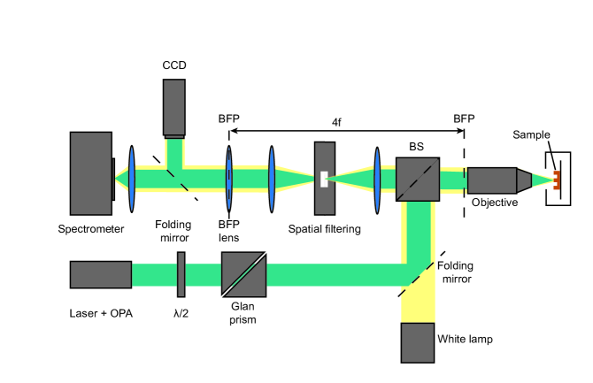
In order to study leaky optical modes of the fabricated PCSs, we perform angle-resolved spectroscopy measurements based on the back focal plane (BFP) setup. The BFP of the objective lens (Mitutoyo NIR 50 with an N.A. of 0.55) is imaged on a slit spectrometer coupled to a liquid nitrogen-cooled imaging CCD camera (Princeton Instruments SP2500+PyLoN) using the 4f scheme (see SI for the details). For the illumination of the sample as well as for the measurements of the reflectance spectra, a halogen lamp is used. The plane of incidence contains both normal to the sample and the direction of periodicity of the PCS (see Fig. 1a). Before impinging the slit of the imaging spectrometer, light reflected from the sample passes through a linear polarizer aligned such that TE modes are studied. The scheme is also used to obtain the angle-resolved photoluminescence spectra using a femtosecond laser (Pharos, Light Conversion) coupled with a broad-bandwidth optical parametric amplifier (Orpheus-F, Light Conversion) at the wavelength of 480 nm, 100 kHz repetition rate as a non-resonant excitation source. All measurements were performed at a room temperature of 300K.
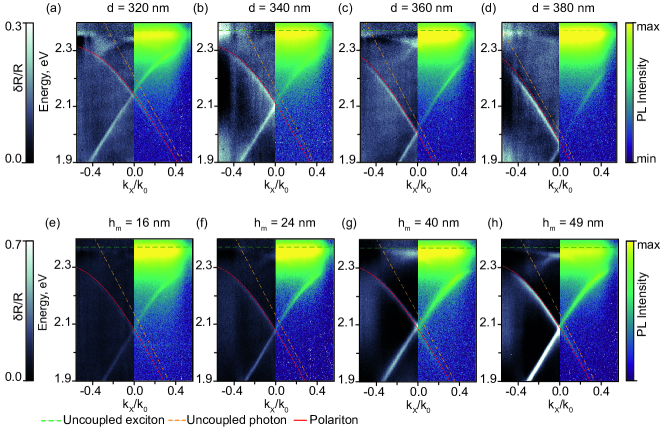
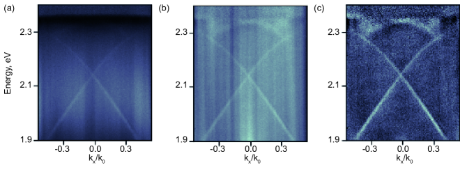
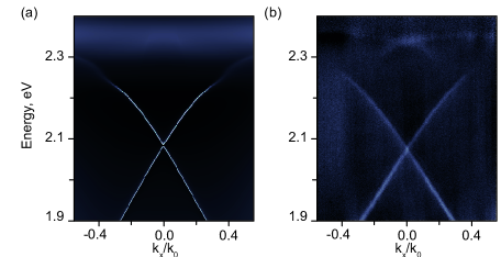
We measure angle-resolved reflectance and photoluminescence spectra for every of the fabricated PCSs, shown in Fig. 3. The measured data show the pronounced leaky modes in the spectral region below the exciton resonance around 2.37 eV. All the studied samples demonstrate the curving of the mode dispersion asymptotically approaching the exciton level in the high-frequency region, revealing the signs of the strong light-matter coupling regime.Masharin et al. (2022a)
In order to verify the strong light-matter coupling regime, we extract the modes from the experimental data by the following procedure: first, we subtract the unbound exciton photoluminescence signal from the experimental dispersion at each , then we fit the resulting modes by the peak Lorentz function data. Combining the spectral peak positions for each in-plane wavevector , we obtain the extracted mode dispersion. Since the upper polariton branch (UPB) above the exciton resonance does not exist due to the strong non-radiative absorption, the only way to confirm the strong light-matter coupling regime is to fit the extracted mode with a lower polariton branch (LPB), estimated by the two-coupled oscillator model asHopfield (1958):
| (1) |
where is complex energy accounting for the spectral position and the linewidth of the uncoupled exciton resonance, is the complex dispersion of the uncoupled cavity photon mode, - is a light-matter coupling coefficient. The Rabi splitting corresponds to the minimal energy distance between UPB and LPB, however, as UPB does not exist, we can only estimate this value based on the described model:
| (2) |
The uncoupled photon cavity mode has linear dependence of the energy on the wavenumber since the refractive index is considered to have negligible changes in the considered spectral range without accounting for the exciton resonance. Therefore, we estimate uncoupled photon cavity dispersions as based on the calculations of Fourier modal methodLi (1997) (see SI for details). The coupling coefficient , as well as the half-widths of an unbound photon and exciton , are chosen as the optimization parameters in the fitting of the LPB. The resulting real part of the PL dispersion optimized for each of the samples is shown as red curves in Fig. 3.
The estimated values from the fitting of the uncoupled cavity photon and exciton do not exceed 23 meV and 18 meV, respectively. The resulting values of Rabi splitting for each of the PCSs are shown in Figs. 4e and 4f, which exceed 230 meV for all PCS modulations. The obtained values satisfy the strong light-matter regime criteria (; )Schneider et al. (2018) with a margin in all studied samples.
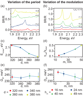
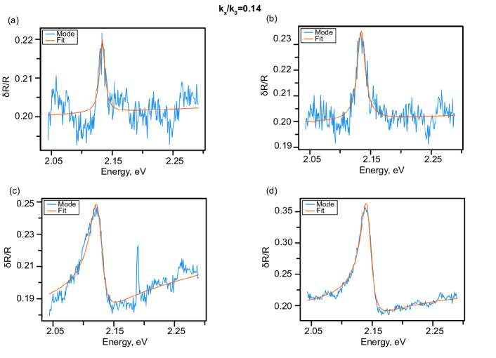
The leaky mode dispersion of the 1D PCS is determined by the waveguide modes folded towards the first Brillouin zone with the edges of , where is a PCS period. For a planar waveguide with the chosen thickness, with the change of the PCS period, the spectral position of folded uncoupled leaky modes, and, hence, polariton branches shift proportionally. Gerace and Andreani (2004) Actually the difference in the spectral position of the polariton modes can be noticed in Figs. 3(a-d). In order to reveal the dependence of the spectral position of polariton mode as a function of period, we extract the reflection spectra at normal incidence (Fig. 4a). The frequencies of the modes are estimated by fitting with the Fano resonance functionMiroshnichenko, Flach, and Kivshar (2010); Fano (1961); Fan, Suh, and Joannopoulos (2003) (See SI for details) and as expected show a monotonous decrease with the increase of PCS period (Fig. 4c).
The value of the Rabi splitting depends on the coupling coefficient and the linewidths of uncoupled exciton and cavity photon modes (Eq. 2). Since the coupling coefficient, depends on the cavity mode localization and oscillator strengthHopfield (1958); Gambino et al. (2014), it should not change strongly with the PCS period or other geometrical parameters. This was confirmed by the results of fitting all the experimental data. In turn, the uncoupled exciton linewidth is the property of the material and thus should not depend on the PCS design, which we also confirmed by analyzing the data. Hence, the only way to tune the Rabi splitting is to vary the radiative part of leaky mode losses , which is dictated by the PCS modulation. Thus, with the variation of the PCS period, we do neither expect nor observe the pronounced dependence of the estimated Rabi splitting values (Fig. 4e).
The variation of the modulation with constant period provides the change in differential reflection contrast of the experimentally measured polariton modes, as shown in Figs. 3e-h and Fig. 4b. Higher modulation causes higher coupling of the leaky mode with the free space, or in other words, increases the radiative losses of the mode. In order to reveal the dependence, we estimate the ratio by fitting the amplitude and asymmetry parameter of the Fano resonance (See SI for details) for different modulations at the = 0.14 and show it in Fig. 4d. Note that the non-radiative losses should be nearly constant for each of the PCSs because they are mostly dictated by the material defect states and excitonic absorption. Hence, the total optical losses rise with increasing the PCS modulation, which leads to the moderate reduction of the Rabi splitting value (Fig. 4f). Thus by applying the different forces on the cantilever during the m-SPL process it is possible to control the modes contrast and the value of the Rabi splitting in the planar exciton-polariton PCS leaky modes.
To conclude, in this work, we have demonstrated the method of mechanical scanning probe lithography for the realization of planar room-temperature exciton-polariton systems based on 2D perovskites. The fabricated PCSs support the long-living polariton modes with a Q-factor up to 100. Thanks to the flexibility of the m-SPL method, it is possible to vary the modulation of the structures with a few tens of nanometers precision. The period of the PCS is controlled with nanometer precision. The width of the trenches is tens of nanometers. In this way, we have achieved full control the dispersion, optical radiative losses, and the Rabi splitting of the exciton-polariton states in the planar photon cavity based on (PEA)2PbI4. Note that the demonstrated method can be introduced for other halide perovskites and for the fabrication of other planar photon cavities, including metasurfaces and PCSs. Our work reveals the affordable for research purposes and time-efficient method for the fabrication of planar high optical quality exciton-polariton systems based on 2D perovskite film, which is highly demanded for the realization of non-equilibrium exciton-polariton condensation in perovskite metasurfaces Masharin et al. (2023) and optical nonlinear and active on-chip polaritonic devices.
Supplementary Information
See supplementary information for more details on the surface morphology of the perovskite films, geometrical and mechanical properties of tip for m-SPL, description of the experimental setup, information on the processing of experimental data, fitting of polariton modes, and errors of the extracted qualities.
Acknowledgements.
The authors thank Rumon Miah for the SEM characterization of the samples. The experimental part of this work was funded by the Russian Science Foundation, grant #21-12-00218 and Ministry of Science and Higher Education of the Russian Federation (Project 075-15-2021-589). A.S. acknowledges the Deutsche Forschungsgemeinschaft (Grant SFB TRR142/project A6), the Mercur Foundation (Grant Pe-2019–0022), and TU Dortmund core funds.References
- Bélanger, Villeneuve, and Aitchison (1997) N. Bélanger, A. Villeneuve, and J. Aitchison, “Solitonlike pulses in self-defocusing algaas waveguides,” JOSA B 14, 3003–3012 (1997).
- Kavokin et al. (2017) A. V. Kavokin, J. J. Baumberg, G. Malpuech, and F. P. Laussy, Microcavities, Vol. 21 (Oxford university press, 2017).
- Weisbuch et al. (1992) C. Weisbuch, M. Nishioka, A. Ishikawa, and Y. Arakawa, “Observation of the coupled exciton-photon mode splitting in a semiconductor quantum microcavity,” Physical Review Letters 69, 3314 (1992).
- Bajoni et al. (2008) D. Bajoni, P. Senellart, E. Wertz, I. Sagnes, A. Miard, A. Lemaître, and J. Bloch, “Polariton laser using single micropillar gaas- gaalas semiconductor cavities,” Physical review letters 100, 047401 (2008).
- Kasprzak et al. (2006) J. Kasprzak, M. Richard, S. Kundermann, A. Baas, P. Jeambrun, J. M. J. Keeling, F. Marchetti, M. Szymańska, R. André, J. Staehli, et al., “Bose–einstein condensation of exciton polaritons,” Nature 443, 409–414 (2006).
- van Vugt et al. (2006) L. K. van Vugt, S. Rühle, P. Ravindran, H. C. Gerritsen, L. Kuipers, and D. Vanmaekelbergh, “Exciton polaritons confined in a zno nanowire cavity,” Physical review letters 97, 147401 (2006).
- Semond et al. (2005) F. Semond, I. Sellers, F. Natali, D. Byrne, M. Leroux, J. Massies, N. Ollier, J. Leymarie, P. Disseix, and A. Vasson, “Strong light-matter coupling at room temperature in simple geometry gan microcavities grown on silicon,” Applied Physics Letters 87, 021102 (2005).
- Stepanov et al. (2021) P. Stepanov, A. Vashisht, M. Klaas, N. Lundt, S. Tongay, M. Blei, S. Höfling, T. Volz, A. Minguzzi, J. Renard, et al., “Exciton-exciton interaction beyond the hydrogenic picture in a mose 2 monolayer in the strong light-matter coupling regime,” Physical Review Letters 126, 167401 (2021).
- Kravtsov et al. (2020) V. Kravtsov, E. Khestanova, F. A. Benimetskiy, T. Ivanova, A. K. Samusev, I. S. Sinev, D. Pidgayko, A. M. Mozharov, I. S. Mukhin, M. S. Lozhkin, et al., “Nonlinear polaritons in a monolayer semiconductor coupled to optical bound states in the continuum,” Light: Science & Applications 9, 1–8 (2020).
- Su et al. (2021) R. Su, A. Fieramosca, Q. Zhang, H. S. Nguyen, E. Deleporte, Z. Chen, D. Sanvitto, T. C. Liew, and Q. Xiong, “Perovskite semiconductors for room-temperature exciton-polaritonics,” Nature Materials 20, 1315–1324 (2021).
- Gélvez-Rueda et al. (2020) M. C. Gélvez-Rueda, M. B. Fridriksson, R. K. Dubey, W. F. Jager, W. Van der Stam, and F. C. Grozema, “Overcoming the exciton binding energy in two-dimensional perovskite nanoplatelets by attachment of conjugated organic chromophores,” Nature Communications 11, 1901 (2020).
- Zhao et al. (2018) Y.-Q. Zhao, Q.-R. Ma, B. Liu, Z.-L. Yu, J. Yang, and M.-Q. Cai, “Layer-dependent transport and optoelectronic property in two-dimensional perovskite:(pea) 2 pbi 4,” Nanoscale 10, 8677–8688 (2018).
- Wang et al. (2018) J. Wang, R. Su, J. Xing, D. Bao, C. Diederichs, S. Liu, T. C. Liew, Z. Chen, and Q. Xiong, “Room temperature coherently coupled exciton–polaritons in two-dimensional organic–inorganic perovskite,” ACS nano 12, 8382–8389 (2018).
- Butté et al. (2005) R. Butté, E. Feltin, J. Dorsaz, G. Christmann, J.-F. Carlin, N. Grandjean, and M. Ilegems, “Recent progress in the growth of highly reflective nitride-based distributed bragg reflectors and their use in microcavities,” Japanese journal of applied physics 44, 7207 (2005).
- Su et al. (2020) R. Su, S. Ghosh, J. Wang, S. Liu, C. Diederichs, T. C. Liew, and Q. Xiong, “Observation of exciton polariton condensation in a perovskite lattice at room temperature,” Nature Physics 16, 301–306 (2020).
- Wu et al. (2021) J. Wu, S. Ghosh, R. Su, A. Fieramosca, T. C. Liew, and Q. Xiong, “Nonlinear parametric scattering of exciton polaritons in perovskite microcavities,” Nano Letters 21, 3120–3126 (2021).
- Sturm et al. (2009) C. Sturm, H. Hilmer, R. Schmidt-Grund, C. Czekalla, J. Sellmann, J. Lenzner, M. Lorenz, and M. Grundmann, “Strong exciton-photon coupling in zno based resonators,” Journal of Vacuum Science & Technology B: Microelectronics and Nanometer Structures Processing, Measurement, and Phenomena 27, 1726–1730 (2009).
- Whittaker et al. (2021) C. Whittaker, T. Isoniemi, S. Lovett, P. Walker, S. Kolodny, V. Kozin, I. Iorsh, I. Farrer, D. Ritchie, M. Skolnick, et al., “Exciton–polaritons in gaas-based slab waveguide photonic crystals,” Applied Physics Letters 119, 181101 (2021).
- Masharin et al. (2022a) M. A. Masharin, V. A. Shahnazaryan, F. A. Benimetskiy, D. N. Krizhanovskii, I. A. Shelykh, I. V. Iorsh, S. V. Makarov, and A. K. Samusev, “Polaron-enhanced polariton nonlinearity in lead halide perovskites,” Nano Letters (2022a).
- Koshelev et al. (2018) K. Koshelev, S. Lepeshov, M. Liu, A. Bogdanov, and Y. Kivshar, “Asymmetric metasurfaces with high-q resonances governed by bound states in the continuum,” Physical review letters 121, 193903 (2018).
- Ardizzone et al. (2022) V. Ardizzone, F. Riminucci, S. Zanotti, A. Gianfrate, M. Efthymiou-Tsironi, D. Suàrez-Forero, F. Todisco, M. De Giorgi, D. Trypogeorgos, G. Gigli, et al., “Polariton bose–einstein condensate from a bound state in the continuum,” Nature 605, 447–452 (2022).
- Alias et al. (2015) M. S. Alias, I. Dursun, D. Shi, M. I. Saidaminov, E. M. Diallo, D. Priante, T. K. Ng, O. M. Bakr, and B. S. Ooi, “Focused-ion beam patterning of organolead trihalide perovskite for subwavelength grating nanophotonic applications,” Journal of Vacuum Science & Technology B, Nanotechnology and Microelectronics: Materials, Processing, Measurement, and Phenomena 33, 051207 (2015).
- Lamers, Zhang, and Wallentin (2022) N. Lamers, Z. Zhang, and J. Wallentin, “Perovskite-compatible electron-beam-lithography process based on nonpolar solvents for single-nanowire devices,” ACS applied nano materials 5, 3177–3182 (2022).
- Zhizhchenko et al. (2021) A. Y. Zhizhchenko, A. B. Cherepakhin, M. A. Masharin, A. P. Pushkarev, S. A. Kulinich, A. A. Kuchmizhak, and S. V. Makarov, “Directional lasing from nanopatterned halide perovskite nanowire,” Nano Letters 21, 10019–10025 (2021).
- Masharin et al. (2022b) M. A. Masharin, V. A. Shahnazaryan, I. V. Iorsh, S. V. Makarov, A. K. Samusev, and I. A. Shelykh, “Room-temperature polaron-mediated polariton nonlinearity in mapbbr3 perovskites,” ACS Photonics (2022b).
- Garcia, Knoll, and Riedo (2014) R. Garcia, A. W. Knoll, and E. Riedo, “Advanced scanning probe lithography,” Nature nanotechnology 9, 577–587 (2014).
- Jeon et al. (2014) N. J. Jeon, J. H. Noh, Y. C. Kim, W. S. Yang, S. Ryu, and S. I. Seok, “Solvent engineering for high-performance inorganic–organic hybrid perovskite solar cells,” Nature materials 13, 897–903 (2014).
- Hopfield (1958) J. Hopfield, “Theory of the contribution of excitons to the complex dielectric constant of crystals,” Physical Review 112, 1555 (1958).
- Li (1997) L. Li, “New formulation of the fourier modal method for crossed surface-relief gratings,” JOSA A 14, 2758–2767 (1997).
- Schneider et al. (2018) C. Schneider, M. M. Glazov, T. Korn, S. Höfling, and B. Urbaszek, “Two-dimensional semiconductors in the regime of strong light-matter coupling,” Nature communications 9, 1–9 (2018).
- Gerace and Andreani (2004) D. Gerace and L. C. Andreani, “Gap maps and intrinsic diffraction losses in one-dimensional photonic crystal slabs,” Physical Review E 69, 056603 (2004).
- Miroshnichenko, Flach, and Kivshar (2010) A. E. Miroshnichenko, S. Flach, and Y. S. Kivshar, “Fano resonances in nanoscale structures,” Reviews of Modern Physics 82, 2257 (2010).
- Fano (1961) U. Fano, “Effects of configuration interaction on intensities and phase shifts,” Physical Review 124, 1866 (1961).
- Fan, Suh, and Joannopoulos (2003) S. Fan, W. Suh, and J. D. Joannopoulos, “Temporal coupled-mode theory for the fano resonance in optical resonators,” JOSA A 20, 569–572 (2003).
- Gambino et al. (2014) S. Gambino, M. Mazzeo, A. Genco, O. Di Stefano, S. Savasta, S. Patane, D. Ballarini, F. Mangione, G. Lerario, D. Sanvitto, et al., “Exploring light–matter interaction phenomena under ultrastrong coupling regime,” ACS Photonics 1, 1042–1048 (2014).
- Masharin et al. (2023) M. A. Masharin, A. K. Samusev, A. A. Bogdanov, I. V. Iorsh, H. V. Demir, and S. V. Makarov, “Room-Temperature Exceptional-Point-Driven Polariton Lasing from Perovskite Metasurface,” Adv. Funct. Mater. n/a, 2215007 (2023).
- Ciers et al. (2017) J. Ciers, J. G. Roch, J.-F. Carlin, G. Jacopin, R. Butté, and N. Grandjean, “Propagating polaritons in iii-nitride slab waveguides,” Physical Review Applied 7, 034019 (2017).
- Zhang et al. (2018) L. Zhang, R. Gogna, W. Burg, E. Tutuc, and H. Deng, “Photonic-crystal exciton-polaritons in monolayer semiconductors,” Nature communications 9, 1–8 (2018).
- Schmidt-Grund et al. (2008) R. Schmidt-Grund, B. Rheinländer, C. Czekalla, G. Benndorf, H. Hochmuth, M. Lorenz, and M. Grundmann, “Exciton–polariton formation at room temperature in a planar zno resonator structure,” Applied Physics B 93, 331–337 (2008).
- Makarov et al. (2019) S. Makarov, A. Furasova, E. Tiguntseva, A. Hemmetter, A. Berestennikov, A. Pushkarev, A. Zakhidov, and Y. Kivshar, “Halide-perovskite resonant nanophotonics,” Advanced optical materials 7, 1800784 (2019).
- Steele et al. (2017) J. A. Steele, H. Yuan, C. Y. Tan, M. Keshavarz, C. Steuwe, M. B. Roeffaers, and J. Hofkens, “Direct laser writing of -to -phase transformation in formamidinium lead iodide,” ACS nano 11, 8072–8083 (2017).
- Yi et al. (2017) N. Yi, S. Wang, Z. Duan, K. Wang, Q. Song, and S. Xiao, “Tailoring the performances of lead halide perovskite devices with electron-beam irradiation,” Advanced Materials 29, 1701636 (2017).
- Alias et al. (2016) M. S. Alias, Y. Yang, T. K. Ng, I. Dursun, D. Shi, M. I. Saidaminov, D. Priante, O. M. Bakr, and B. S. Ooi, “Enhanced etching, surface damage recovery, and submicron patterning of hybrid perovskites using a chemically gas-assisted focused-ion beam for subwavelength grating photonic applications,” The journal of physical chemistry letters 7, 137–142 (2016).
- Ivchenko (2005) E. L. Ivchenko, Optical spectroscopy of semiconductor nanostructures (Alpha Science Int’l Ltd., 2005).
[Mechanical scanning probe lithography of 2D perovskites for fabrication of planar polaritonic cavities] Supplementary Materials: Mechanical scanning probe lithography of perovskites for fabrication of high-Q planar polaritonic cavities N. Glebov
M. Masharin
B. BorodinP. Alekseev
F. BenimetskiyS. MakarovA. Samusev*
S1 Surface morphology of the pristine 2D perovskite film
The topographical surface map of the pristine quasi-2D perovskite thin film is shown in Fig. S5a. The topography is obtained by atomic force microscopy (AFM). Structuring by mechanical scanning probe lithography requires the roughness of the sample lower than the assumed modulation of the photonic crystal slab. The roughness can affect the non-uniform broadening of the optical modes, leading to a decrease in the radiative lifetime. Based on the obtained data we estimate the height distribution, shown in Fig. S5b. The width at the half-height of this distribution determines the roughness of the sample. The roughness of the fabricated samples does not exceed 15 nm.
S2 Tip for mechanical scanning probe lithography
For the procedure of mechanical scanning probe lithography, we use an atomic force microscope SMART, cantilevers with a single-crystal diamond tip (TipsNano DRP-IN). The tip with a resonant frequency of 500 – 1000 kHz, a spring constant of 100 – 600 N/m, and a normal spring constant of 350 N/m. Normal spring constants for AFM tips used in experiments were calculated using the Sader methodsader1999calibration. This method allows us to determine the spring constant of an atomic force microscope cantilever using the following parameters: the resonant frequency, the quality factor of the cantilever in air, and their geometrical dimensions. The spring constant is given by:
| (S3) |
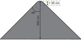
where is the resonant frequency of the cantilever in air, are width and length of the cantilever, is the quality factor, is the density of the air and is the imaginary part of the so-called “hydrodynamic function”green2005frequency. This hydrodynamic function only depends on the Reynolds number , where is the viscosity of the surrounding environment and is independent of the cantilever thickness and density. We experimentally measured parameters such as and for each of cantilever. The physical constants associated with the surrounding environment were taken from the literature: and . Fig. S6 shows schematically the geometry of the tip used. The tip has a conical shape. The radius of curvature of its tip is less than 35 nm. The solution angle is 45 degrees. The height of the tip is () nm. Thus, knowing the geometry of the probe used, it is possible to unambiguously determine the minimum dimensions of the cavities depending on the modulation depth.
S3 Pushing force
For the procedure of mechanical scanning probe lithography, we set the pushing force on the perovskite thin film. It is possible to estimate the pushing force asmironov2004basics:
| (S4) |
where - the cantilever stiffness, - the value characterizing the bending of the cantilever, induced by its shift with respect to the sample along the surface normal. In order to make the PCS with the necessary modulation, the pushing force was selected as follows. With some steps, starting with the minimum pressure for each following structure, we increased the force, until the huge pushing force completely carve the perovskite grains. We estimated the force required to obtain PCS with modulation in the 15-50 nm range based on quasi-two-dimensional perovskite using the probes indicated above for the m-SPL procedure.
S4 Angle-resolved spectroscopy at room temperature
For the optical characterization of photonic crystal slabs (PCS), angle-resolved photoluminescence and reflection spectra were measured using the optical setup shown in Fig. S7. The sample was placed in a chamber with a vacuum pump and optical window. The vacuum pump evacuates air up to pressure around 10-5 bar to avoid the degradation of the perovskite sample from the oxygen. All measurements were carried out at room temperature. (See "optical experiment" section in the main text)
S5 Spectral processing of experimental data
In order to make the angle-resolved reflection spectra more contrast, we perform the data treatment shown in Fig.S8. The first step is to normalize the reflection spectra at each wavenumber by the average value of the spectrum in terms of energy at that wavenumbers (Fig.S8b). The second step is to find a linear function which is an underlying background of the spectra at each wavenumber . Then the spectra at each wavenumber are normalized to the corresponding linear functions and the final data are obtained (Fig.S8c).
S6 Fitting of polariton dispersions
To extract the polariton mode from the angle-resolved photoluminescence spectrum, we first subtract the uncoupled exciton resonance signal from the measured spectrum at each wavenumber and fit the data by a Lorentz peak function. Combining the positions of the peaks at all wavenumbers , we obtain the polariton dispersion. It is possible to estimate the coupling strength between cavity photon and exciton resonance using the fitted bound oscillator Hopfield (1958), a model that takes into account the spectral position and linewidth of the unbound exciton and the photon mode parameters of the unbound cavity . Polariton states are defined as:
| (S5) |
where – is the light-matter coupling strength. To use this model for parameter fitting, it is necessary to estimate the parameters of the uncoupled excitation resonance and photon. The exciton level was found from the reflection spectrum from the unstructured sample. The uncoupled photon parameters for structures with different periods or modulations were determined in different ways. For a period-changing PCS, the slope coefficient of an unbound photon is determined from the calculated dispersion of a polariton by the modal Fourier method Li (1997) (See Fig.S9a).
The slope coefficient was estimated from the extrapolation of the polariton dispersion to large . The free parameter was estimated by the least squares method from fitting the data of experimental polariton dispersions. For a PCS with a change in modulation, the parameters of an unbound photon were estimated from the modal Fourier method. Then were the fitting parameters in the model of two coupled oscillators. After that they were averaged and fixed for all structures.
S7 Fitting polariton modes with the Fano profile
S7.1 Fano resonance in optical cavities
Using the theoretical model of a single-mode optical resonator associated with 2 ports, one can obtain the intensity reflection coefficient:Fan, Suh, and Joannopoulos (2003)
| (S6) |
where and are the center frequency and the lifetime of the resonance, respectively. and are real parameters of S-matrix with . Sign corresponds to the parity of the resonant mode with respect to the mirror plane. In all systems except those with r or t being zero, the spectral profile of the reflectance coefficient has Fano line shape.
S7.2 Fit Fano function with losses
The Fano function with an amplitude coefficient was used to fit the parameters of the exciton-polariton modes in reflection, shown in Fig. S10Fano (1961):
| (S8) |
where B is the amplitude coefficient, q is the phenomenological shape parameter, . is the resonant energy and is the width of the autoionized state. In the limit , the shape of the line is determined by the transition through a discrete state with a Lorentz profile, as the transition to the continuum is very weak Miroshnichenko, Flach, and Kivshar (2010). The total loss can be represented as a sum of radiative and nonradiative losses , then the Lorentz profile can be expressed asIvchenko (2005) :
| (S9) |
The parameters are estimated during the fit by the Fano function of the experimental reflectance spectrum at . We use the limit pass of the Fano resonance to the Lorentz profile to express the ratio of the radiative and total losses.
| (S10) |
| (S11) |
Thus it is possible to relate the fit parameters to the ratio of radiative and total losses:
| (S12) |
S8 Mechanical scanning probe lithography of and
Mechanical scanning probe lithography is an excellent method for structuring other perovskites as well, including 3D perovskites. As an example, the structuring of a thin film of perovskite was carried out (See Fig. S11b).
S9 Errors of the extracted quantities
| Period | Modulation | |||||||
|---|---|---|---|---|---|---|---|---|
| 320 nm | 340 nm | 360 nm | 380 nm | 16 nm | 24 nm | 40 nm | 49 nm | |
| , meV | 240 | 238 | 243 | 241 | 252 | 248 | 240 | 235 |
| RMS error, meV | 6 | 5 | 7 | 10 | 5 | 6 | 10 | 5 |
| , eV | 2.14 | 2.10 | 2.01 | 1.97 | ||||
| RMS error, eV | ||||||||
| 0.14 | 0.19 | 0.24 | 0.40 | |||||
| RMS error | ||||||||