Ferroelectrically switchable magnetic multistates in MnBi2Te4(Bi2Te3)n and MnSb2Te4(Sb2Te3)n ( = 0, 1) thin films
Abstract
Ferroelectric control of two-dimensional magnetism is promising in fabricating electronic devices with high speed and low energy consumption. The newly discovered layered MnBi2Te4(Bi2Te3)n and their Sb counterparts exhibit A-type antiferromagnetism with intriguing topological properties. Here, we propose to obtain tunable magnetic multistates in their thin films by ferroelectrically manipulating the interlayer magnetic couplings (IMCs) based on the Heisenberg model and first-principles calculations. Our strategy relies on that interfacing the thin films with appropriate ferroelectric materials can switch on/off an interlayer hopping channel between Mn- orbitals as the polarizations reversed, thus resulting in a switchable interlayer antiferromagnetism-to-ferromagnetism transition. On the other hand, the interface effect leads to asymmetric energy barrier heights for the two polarization states. These properties allow us to build ferroelectrically switchable triple and quadruple magnetic states with multiple Chern numbers in thin films. Our study reveals that ferroelectrically switchable magnetic and topological multistates in MnBi2Te4 family can be obtained by rational design for multifunctional electronic devices, which can also be applied to other two-dimensional magnetic materials.
I INTRODUCTION
Two-dimensional (2D) magnetic materials provide an ideal platform to explore novel magnetic and electronic properties [1, 2, 3, 4, 5, 6, 7]. The delicate interlayer exchange couplings in these systems enable a variety of methods of manipulating their magnetism. For instance, recent studies revealed that the A-type antiferromagnetic (AFM) CrI3 bilayer could be tuned into ferromagnetic (FM) by external electric field [8, 9], electrostatic doping [10, 11], and interface engineering [12, 13, 14, 15, 16, 17]. Twisting the bilayer may yield non-collinear magnetism [18, 19, 20].
Recently, the MnBi2Te4 family, i.e., MnBi2Te4(Bi2Te3)n and MnSb2Te4(Bi2Te3)n, which are hereafter referred to as MAT, have attracted much attention due to the coexistence and interesting interplay of intrinsic magnetism and band topology in them [21, 22, 23, 24, 25, 26, 27, 28, 26, 29, 30, 31, 32, 33, 34, 35, 36, 37, 38]. This series of materials also have a layered van der Waals (vdW) structure with the A-type AFM structure as revealed by experiments [39, 40, 41, 42], which preserves the combination of the time-reversal and a half lattice translation symmetry. As a result, many of them show nontrivial topological properties such as topological insulators [21] and axion insulators [22]. Moreover, the systems can also be turned into Weyl semimetals as the interlayer couplings become ferromagnetic [22, 23, 36].
The A-type AFM coupling in MAT yields unusual even-odd layer-number dependent magnetism for their thin films [43, 35, 44]. The even-number (even-) systems are expected to have no net magnetization. Whereas those with odd-number (odd-) layers have uncompensated magnetization. This difference can lead to distinct topological properties for them. For instance, the thin films of MnBi2Te4 with odd- septuple layers are quantum anomalous Hall insulators. However, those with even- layers have a zero Chern number[43]. Instead, their topological properties can be characterized by the so-called pseudospin Chern number[45]. Due to the weak interlayer interaction, small magnetic fields could induce spin-flip transitions, giving rise to an AFM-to-FM transition in the IMCs [41, 35]. Chemical dopings [46, 47] and antisite defects [48, 49, 50, 51, 52] can also be used to manipulate the IMCs in these systems, although they may complicate the nature of the surface states. First-principles calculations suggest that the AFM double-septuple MnBi2Te4 could be driven into a Chern insulator with a high Chern number under electric fields [53], and could be driven into FM IMCs by interfacing with monolayers of transition-metal dichalcogenide and h-BN [54].
In this paper, we propose to ferroelectrically tune the IMCs in MnBi2Te4(Bi2Te3)n and MnSb2Te4(Sb2Te3)n ( = 0 and 1) thin films for magnetic multistates by interface, which is desired for memory devices with high density storage, high speed, and low power consumption. We reveal that hole doping can lead to an interlayer AFM-to-FM transition in MAT bilayers based on the understanding of the IMCs using the Heisenberg model. We provide a guideline for designing ferroelectric substrates that may induce transitions in the interlayer exchange couplings, i.e., polarization dependent IMCs, as demonstrated by our first-principles calculations. Moreover, we find that the interface effect results in symmetry breaking in the two polarization states of the FE substrate. This asymmetry allows us to design switchable magnetic multistates in sandwich structures made of MnBi2Te4 multilayers and 2D ferroelectric (FE) materials, which also exhibit distinct electronic and topological properties.
II COMPUTATIONAL DETAILS
We perform DFT calculations for our systems using the Vienna Ab initio Simulation Package [55]. The pseudopotentials were constructed by the projector augmented wave method [56, 57]. An 11 11 1 and 21 21 1 -centered -mesh were used to sample the 2D Brillouin zone for structural relaxation and electronic structure calculations, respectively. The plane-wave energy cutoff is set to 400 eV for all calculations. A 20 Å vacuum region was used between adjacent plates to avoid the interaction between neighboring periodic images. Van der Waals (vdW) dispersion forces between the adsorbate and the substrate were accounted for through the DFT-D3 [58]. Different vdW methods/functionals such as DFT-D2 and optPBE-vdW were also used for comparison [59, 60, 61]. The systems were fully relaxed until the residual force on each atom is less than 0.01 eV/Å. The DFT+U method [62] is used to treat electron correlations due to the partially filled -orbital of Mn for which a value of 5.34 eV is used [21]. Our results on the structural properties, magnetism, and band structures of the free-standing MAT films are consistent with previous studies [21, 36, 32]. The kinetic pathways of transitions between different polarization states are calculated using the climbing image nudge elastic band (CI-NEB) method [63, 64]. The topological properties calculations were done using the WANNIER90 [65] and WannierTools package [66].
III RESULTS AND DISCUSSIONS
III.1 Concept of ferroelectric tuning of IMCs in MAT bilayers
We begin by presenting the concept of FE tuning of IMCs in MAT bilayers, which is shown in Fig. 1. In these systems, each Mn atom is coordinated with six chalcogen atoms, which form a distorted octahedron. The Mn-3 orbitals are split into triply degenerate states and the doubly degenerate states due to the octahedral ligand field. The states are further split due to the magnetic exchange interaction between the Mn atoms. As a result, the majority states of the and orbitals are fully occupied by the five electrons of the Mn2+ ions (see Fig. 1), resulting in a high spin state for the Mn2+ ions. Like the 2D magnetic bilayers reported by Refs 31, 67, this type of occupation favors AFM IMCs between the Mn+2 ions, which are mediated by the -orbitals of the nonmetallic atoms (denoted by ). Whereas FM IMCs are energetically unfavorable because the hopping between the Mn- orbitals of adjacent layers is prohibited [31, 67, 68]. For our systems, reducing the occupation of the orbitals makes the hopping channel energetically favorable, thus enhancing the stability of the FM IMCs. Indeed, our DFT calculations indicate that all the MAT bilayers undergo the AFM-to-FM transition by small hole dopings (see Fig. 1c and Fig. S1[69]), which is also expected for their multilayers.
The IMCs in MAT-2L can be understood using the following spin Hamiltonian.
| (1) |
where and denote the intra- and interlayer exchange interactions between the Mn ions, respectively. The intralayer ones are denoted by for the top layer and for the bottom layer, for which only the first nearest-neighbor interactions are taken into account. are equal to for the freestanding MAT-2L. Whereas for the interlayer ones, the second nearest neighbors are included. For the bilayers without doping, we obtain positive and negative (see Fig. 1d, Fig. S2 and Table S1[69]). Note that the magnitude of is larger than that of . So, the sum of and , i.e., , is positive, which gives rise to AFM IMCs. Introducing hole doping suppresses while enhances . As a result, decreases with increasing of the hole doping and eventually changes its sign across the AFM-to-FM transition (see Fig. 1d).
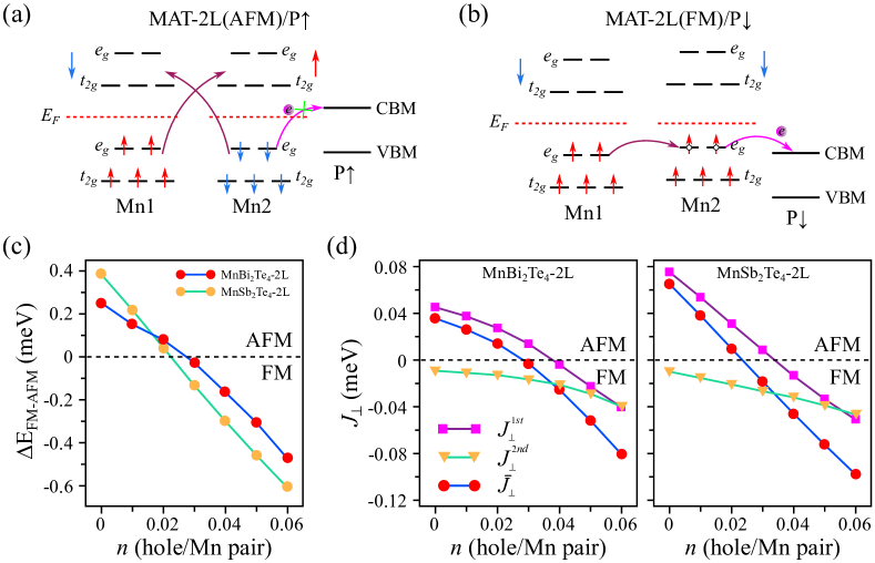
Experiments find that most of MnA2Te4(A2Te3)n (A = Bi, Sb; = 0 2) show n-type metallic conductivity mainly due to the existence of antisite mixing of A and Mn[28, 40, 48, 49, 70, 47], which is unfavorable for the FM IMCs. Doping with Sb can induce a n-to-p transition in the carrier type[48, 70, 47]. However, different groups report different IMCs at high concentrations of Sb, e.g., MnSb2Te4. Both AFM and FM IMCs were reported by previous studies, which suggests that the IMCs in this family are strongly dependent on the growth condition[48, 70, 47]. In addition, recent experiment finds that doping of Sb at = 0.25 can give rise to an AFM-to-FM transition in the interlayer couplings for For Mn(Bi1-xSbx)6Te10 [47, 71]. For the MAT thin films, the hole doping can also be achieved via interfacial charge transfer which requires suitable band alignments between them and the substrates. When their bands are in the type-I or type-II alignment, interfacial charge transfer can be negligible. In these cases, the IMCs are most likely to be AFM. In contrast, electrons will be transferred from the MAT bilayer to the substrate when they are in the type-III band alignment that the valence band maximum (VBM) of the MAT bilayer are higher than the conduction band minimum (CBM) of the substrate. Namely, hole doping is introduced to the MAT bilayer, which is desired for the AFM-to-FM transition. Ferroelectrically switchable IMCs may be achieved if a 2D FE materials serves as the substrate so that reversing its polarizations gives rise to a switching of the band alignment from type-III to type-I (II) or vice versa (see Fig. 1). However, one can expect that the transferred electrons mainly come from the interfacial MAT layer because of the vdW-type interlayer bonding. Therefore, the spin-flipping most likely happen to the interfacial MAT layer rather than those further away from the substrate.
III.2 MAT-2L/In2Se3 heterostructures
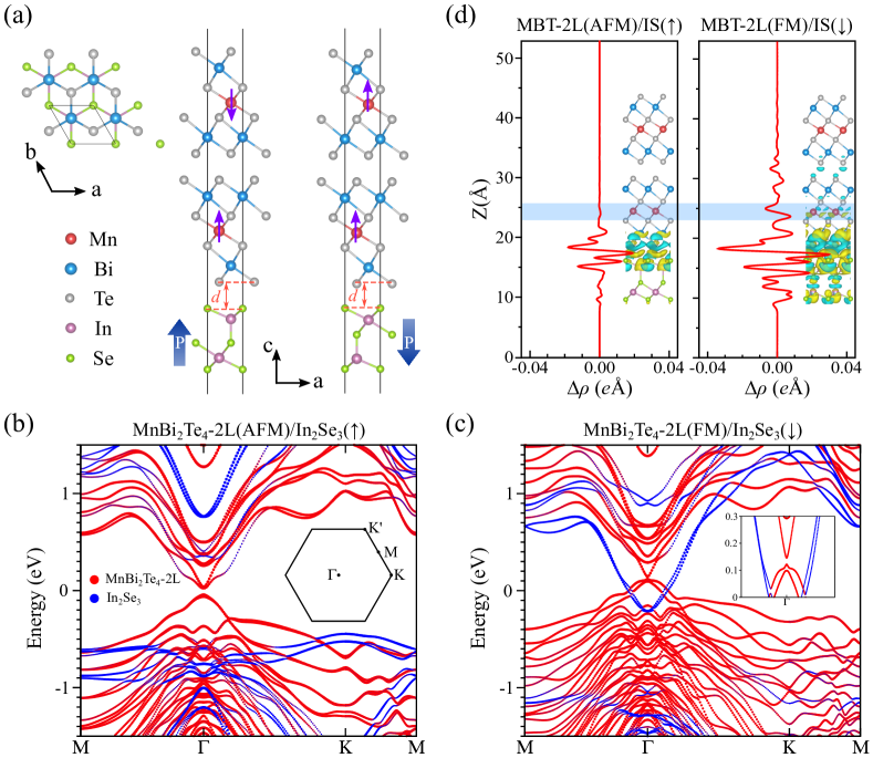
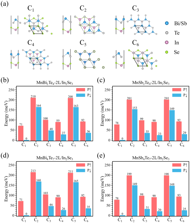
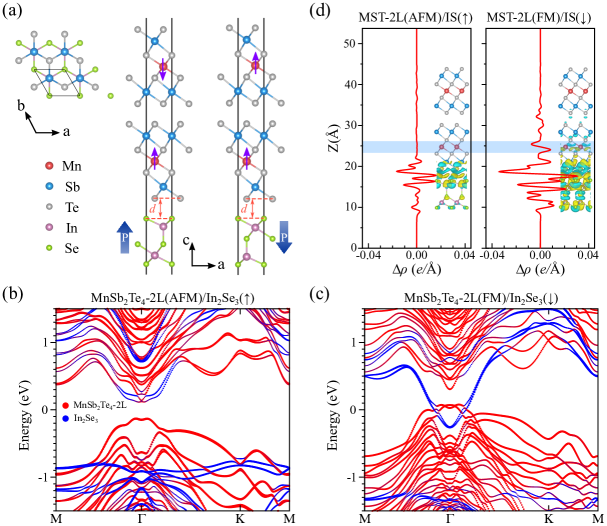
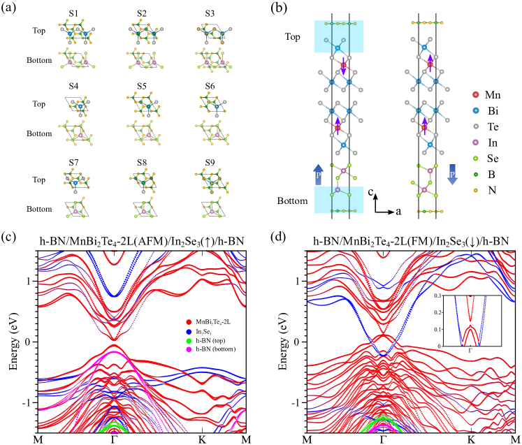
We now come to first-principles calculations of the heterostructures of MAT thin films and 2D FE materials. We choose In2Se3 monolayer as the substrate, which has been experimentally proved since its prediction in 2017 [72, 73, 74]. We applied the same way for the structural modelings of the heterostructures as Ref. 75, that is, the lattice constants of MAT thin fimls are fixed, whereas that of In2Se3 is adjusted to match those of the overlayers. We have performed careful calculations over a number of stacking configurations (see Fig. S3 and Table S2 [69] ). The lowest energy configuration is shown in Fig. 2a, in which the interfacial Se and Te are in the hollow sites. The stacking order is the same as the one for MnBi2Te4 monolayer on In2Se3 [75], which shows up for all MAT bilayers on In2Se3. Table 1 summarizes the stability of the two magnetic states for MAT bilayers on In2Se3 monolayer in different polarization states. One can see that for all the MAT bilayers the IMCs remain AFM when the polarization is pointing toward the interface, but become FM as the polarization is reversed. The trend is independent of the vdW functionals/methods (Table S3 [69]).
| Systems | [meV/(Mn pair)] | IMCs |
| MnBi2Te4-2L | 0.21 | AFM |
| MnBi2Te4-2L/In2Se3() | 0.22 | AFM |
| MnBi2Te4-2L/In2Se3() | -0.16 | FM |
| MnSb2Te4-2L | 0.39 | AFM |
| MnSb2Te4-2L/In2Se3() | 0.36 | AFM |
| MnSb2Te4-2L/In2Se3() | -0.40 | FM |
| MnBi4Te7-2L | 0.03 | AFM |
| MnBi4Te7-2L/In2Se3() | 0.03 | AFM |
| MnBi4Te7-2L/In2Se3() | -0.01 | FM |
| MnSb4Te7-2L | 0.06 | AFM |
| MnSb4Te7-2L/In2Se3() | 0.09 | AFM |
| MnSb4Te7-2L/In2Se3() | -0.04 | FM |
Below we focus on the electronic structure of MnBi2Te4 bilayer on In2Se3 monolayer, i.e., MnBi2Te4-2L/In2Se3, which are shown in Figs. 2b-d. Those for all other MAT systems are shown in Figs. S4S6 since they show pretty much the same trend as MnBi2Te4-2L/In2Se3. The Fermi level is located in the band gap for the AFM state. Whereas for the FM state, the conduction band of In2Se3 is shifted down into the valence band of MnBi2Te4-2L such that the Fermi level is crossing the valence band of the latter. This feature favors interfacial charge transfer. Fig. 2d depicts the differential charge density for the two magnetic states, which indicates that there is almost negligible interfacial charge transfer between the MnBi2Te4-2L and In2Se3 for the AFM state. In contrast, the charge transfer is much more significant for the FM state than that for the AFM state. A close inspection finds that the charge density on the Mn atoms in the interfacial layer becomes positive. This confirms the picture of hole doping over this layer and opens up the hopping channel. Consequently, the FM state becomes energetically favorable for this type of band structure. Thus, the FE In2Se3 monolayer fits the criterion for a substrate that gives switchable band alignments between type-II and type-III with MnBi2Te4-2L. The switchable band alignments induced by a monolayer of FE In2Se3 are robust and unchanged by the use of the HSE06 hybrid functional in the calculations (see Figs. S7[69]). Moreover, the trend that the charge transfer mainly happened to the interfacial layer also suggests that the spin-flipping accompanied by the AFM-FM transition takes place to the interfacial MnBi2Te4 layer. For the trilayers and quadlayers, our calculations find the same trend in the spin-flipping as the bilayers (Figs. S8S9[69]). We further investigate the effect of substrates on the IMCs in the heterojunctions MnBi2Te4-2L/In2Se3. We chose h-BN as the substrate to construct the sandwich heterojunction of h-BN/MnBi2Te4-2L/In2Se3/h-BN since it has been widely used as a capping layer in devices. Our result show that h-BN has minor effect on the energy difference between the interlayer FM and AFM states (Table S4[69]), as well as the band alignment between MnBi2Te4-2L and In2Se3 (Fig. S10 [69]).
III.3 Magnetic multistates in MAT multilayers
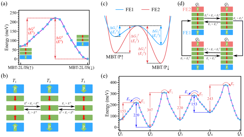
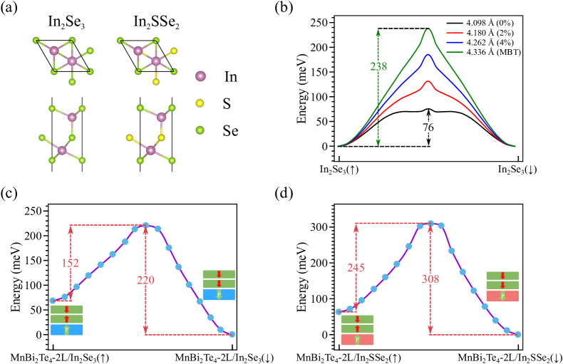
The interface has a significant impact on the polarization states of the FE In2Se3 monolayer by introducing a coupling between its polarizations and the local dipoles of MAT. This coupling breaks the symmetry of the two polarization states, that is, it gives rise to asymmetric barrier heights for the two polarization states. Fig. 3a shows that the state with the polarizations pointing toward the MnBi2Te4 bilayer has a barrier height of about 152 meV (), which is about 68 meV lower than the one with polarizations pointing away from the interface (). The barriers shown in Fig. 3a larger than that reported by Ref. 72 is due to the strain effect (see Fig. S11 [69]). Nevertheless, our results reveal asymmetry in the energy barriers. Therefore, the critical electric fields needed to flip the polarizations pointing toward the interface () is smaller than that for the reverse process (), i.e., . In Fig. 3a, we assume that the initial AFM ordering in the MnBi2Te4 bilayer is head-to-head. This configuration has almost the same energy as the one with tail-to-tail magnetizations in the case that magnetic anisotropy is not included (The magnetic anisotropy is pretty small, see Ref. 75).
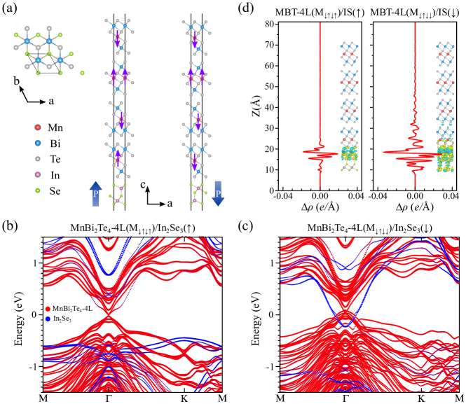
The asymmetric barrier heights along with the unique polarization-dependent IMCs allow designing ferroelectrically switchable magnetic multistates for MAT multilayers. We illustrate the concept in MnBi2Te4 trilayers and quadlayers, i.e., MnBi2Te4-3L and MnBi2Te4-4L. We first sandwich MnBi2Te4-3L in between two In2Se3 layers (Fig. 3b). Suppose that both the top and bottom In2Se3 layers have up polarizations, which can be achieved by applying external electric fields anyway. According to the polarization dependent IMCs discussed above, spins in the MnBi2Te4 layer next to the top In2Se3 layer will be flipped so that it will be ferromagnetically coupled with the underneath MnBi2Te4 layer. We label this magnetic state as . Then one can apply an electrical field antiparallel to the axis that is larger than the critical field overcoming but smaller than the one required to overcome , i.e., . As a result, the polarizations in the bottom layer will be reversed while those in the top layer will remain unchanged. Then, the magnetization of the bottom MnBi2Te4 layer will be flipped to be ferromagnetically coupled with the adjacent MnBi2Te4 layer, i.e., in Fig. 3b. Further increasing the electric field such that will also drive the polarizations of the top In2Se3 layer to be flipped. Correspondingly, the magnetizations of the top MnBi2Te4 layer will be flipped, for which the magnetic state is labelled as . Now, an electric field along the axis, i.e., , will first force the polarization of the bottom In2Se3 to be reversed when . As a result, the system will flow into . Further enhancing to the level that will drive the system back into . So the whole system have triple magnetic states, which can be ferroelectrically controlled. Likewise, sandwiching thicker films than triple layers by the same FE layers also gives rise to triple magnetic states.
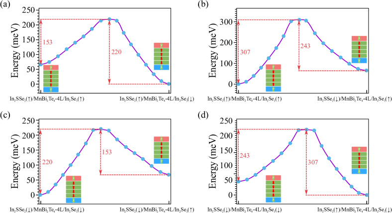
More magnetic states can be obtained by sandwiching the MAT thin films in between two different FE layers with a special combination of the barrier heights. Such a combination requires that the highest barrier for one FE monolayer should be lower than the lowest barrier for the other FE layer. We depict the barrier heights for the two different FE layers in Fig3c, and are for one FE layer (FE1), to which the corresponding critical electric fields are and , respectively. Whereas and are for the other layer colored in red (FE2), for which the critical fields are and , respectively. In the case that , i.e., , a layer-by-layer flipping mechanism for the FE contacts can be achieved by properly controlling the electric field. As a result, one can have quadruple magnetic states based on the polarization-dependent IMCs in MAT heterostructures (Fig. 3d). Our calculations find that the barrier heights of In2Se3 and In2SSe2 monolayers fit the above requirement for the quadruple magnetic states. Specifically, we obtain 245 meV () and 308 meV () for In2SSe2 with polarizations pointing toward and away from the MnBi2Te4 layer (see Figs. S11 and S12 [69]), respectively, which are larger than those of In2Se3 (see Fig. 3a, 152 meV for and 220 meV for ). In Fig. 3e, we show the kinetic pathway of transforming the polarization states, which suggests that the quadruple states are ferroelectrically switchable.
III.4 Topological properties of MAT thin films
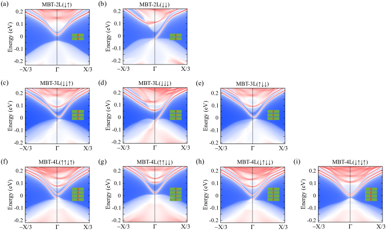
The ferroelectrically tunable magnetic multistates give rise to a variety of distinct topological properties for the MAT thin films. In MAT systems, each helical surface state contribute half-quantized Hall conductance. So, the Chern number () will be 0 when magnetizations of the two surfaces of the thin film are antiparallel, and will be 1/-1 when the surface magnetizations are parallel with up/down spin-polarizations. Therefore, according to our results shown in Fig. 3, there are two different Chern numbers for In2Se3/MnBi2Te4-3L/In2Se3 and In2Se3/MnBi2Te4-4L/In2Se3, and three Chern numbers for In2SSe2/MnBi2Te4-4L/In2Se3, respectively. We perform calculations of the Chern number for the MnBi2Te4 multilayers with the magnetic states shown in Figs. 2 and 3. For the bilayer systems, the topological properties of MnBi2Te4 remain unchanged upon interfacing, i.e., for the FM state and for the AFM state, which is also supported by the results of edge states (Figs. S13 and S14). For MnBi2Te4-3L, we have = 0, -1, and 0 for , , and , respectively. Whereas for MnBi2Te4-4L, there are three Chern numbers for the quadruple states, i.e., 1, 0, and -1. Table 2 summarizes the Chern numbers for the studied MnBi2Te4 thin films. We expect that such a ferroelectrically tunable multiplet for the Chern number may be seen in other MAT multilayers.
| Systems | IMCs | |
| MnBi2Te4-2L | M1 () | 0 |
| M2 () | -1 | |
| MnBi2Te4-3L | T1 () | 0 |
| T2 () | -1 | |
| T3 () | 0 | |
| MnBi2Te4-4L | Q1 () | 1 |
| Q2 () | 0 | |
| Q3 () | -1 | |
| Q4 () | 0 |
In conclusion, we have proposed to ferroelectrically tune the magnetism of MAT thin films using model and first-principles calculations. The scheme is based on the fact that the IMCs are strongly dependent on the occupation of -orbitals of the Mn2+ ions. The variation in the occupation can be controlled by interfacing the films with a FE layer with appropriate band alignments. We have demonstrated the concept in MAT/In2Se3 heterostructures by performing first-principles calculations. We find that the interfacing effect mainly has an impact on the interfacial MAT layer. Specifically, there is spin-flipping in the interfacial layer when polarizations of the In2Se3 are reversed, which results in ferroelectrically switchable IMCs and an AFM-to-FM transition. On the other hand, the interfacing effect leads to asymmetric energy barrier heights, which means that different electric fields are needed to switch the polarizations for the two states. We further show that this physics can be used to build magnetic multistates in their sandwich structures. Our calculations suggest that triple and quadruple magnetic states with tunable Chern number can be obtained for MnBi2Te4 thin films by sandwiching them in between appropriate FE layers. Our results will not only attract experimental interest in FE control of the magnetism and topological properties of MAT thin films, but also inspire designing novel magnetism in other 2D materials.
Acknowledgements.
We thank Haijun Zhang and Zhixin Guo for useful discussions. This work was supported by the National Natural Science Foundation of China (Grants No. 12174098, No. 11774084, No. U19A2090 and No. 91833302) and project supported by State Key Laboratory of Powder Metallurgy, Central South University, Changsha, China.References
- Huang et al. [2017] B. Huang, G. Clark, E. Navarro-Moratalla, D. R. Klein, R. Cheng, K. L. Seyler, D. Zhong, E. Schmidgall, M. A. McGuire, D. H. Cobden, W. Yao, D. Xiao, P. Jarillo-Herrero, and X. Xu, Layer-dependent ferromagnetism in a van der Waals crystal down to the monolayer limit, Nature 546, 270 (2017).
- Gong et al. [2017] C. Gong, Z. Li, H. Ji, A. Stern, Y. Xia, W. Bao, Y. Wang, Z. Q. Qiu, R. J. Cava, S. G. Louie, J. Xia, and X. Zhang, Discovery of intrinsic ferromagnetism in two-dimensional van der Waals crystals, Nature 546, 265 (2017).
- Fei et al. [2018] Z. Fei, B. Huang, P. Malinowski, W. Wang, T. Song, J. Sanchez, W. Yao, D. Xiao, X. Zhu, A. F. May, W. Wu, D. H. Cobden, J.-H. Chu, and X. Xu, Two-dimensional itinerant ferromagnetism in atomically thin Fe3GeTe2, Nat. Mater. 17, 778 (2018).
- Burch et al. [2018] K. S. Burch, D. Mandrus, and J.-G. Park, Magnetism in two-dimensional van der Waals materials, Nature 563, 47 (2018).
- Gong and Zhang [2019] C. Gong and X. Zhang, Two-dimensional magnetic crystals and emergent heterostructure devices, Science 363, eaav4450 (2019).
- Wang et al. [2021] L. Wang, Y. Shi, M. Liu, A. Zhang, Y.-L. Hong, R. Li, Q. Gao, M. Chen, W. Ren, H.-M. Cheng, Y. Li, and X.-Q. Chen, Intercalated architecture of MA2Z4 family layered van der Waals materials with emerging topological, magnetic and superconducting properties, Nat. Commun. 12, 2361 (2021).
- Ni et al. [2021] J. Y. Ni, X. Y. Li, D. Amoroso, X. He, J. S. Feng, E. J. Kan, S. Picozzi, and H. J. Xiang, Giant Biquadratic Exchange in 2D Magnets and Its Role in Stabilizing Ferromagnetism of Monolayers, Phys. Rev. Lett. 127, 247204 (2021).
- Huang et al. [2018] B. Huang, G. Clark, D. R. Klein, D. MacNeill, E. Navarro-Moratalla, K. L. Seyler, N. Wilson, M. A. McGuire, D. H. Cobden, D. Xiao, W. Yao, P. Jarillo-Herrero, and X. Xu, Electrical control of 2D magnetism in bilayer CrI3, Nat. Nanotechnol. 13, 544 (2018).
- Xu and Zou [2020] R. Xu and X. Zou, Electric Field-Modulated Magnetic Phase Transition in van der Waals CrI3 Bilayers, J. Phys. Chem. Lett. 11, 3152 (2020).
- Jiang et al. [2018] S. Jiang, L. Li, Z. Wang, K. F. Mak, and J. Shan, Controlling magnetism in 2D CrI3 by electrostatic doping, Nat. Nanotechnol. 13, 549 (2018).
- Soriano and Katsnelson [2020] D. Soriano and M. I. Katsnelson, Magnetic polaron and antiferromagnetic-ferromagnetic transition in doped bilayer CrI3, Phys. Rev. B 101, 041402 (2020).
- Lu et al. [2020] Y. Lu, R. Fei, X. Lu, L. Zhu, L. Wang, and L. Yang, Artificial Multiferroics and Enhanced Magnetoelectric Effect in van der Waals Heterostructures, ACS Appl. Mater. Interfaces 12, 6243 (2020).
- Cheng et al. [2021] H.-X. Cheng, J. Zhou, C. Wang, W. Ji, and Y.-N. Zhang, Nonvolatile electric field control of magnetism in bilayer on monolayer , Phys. Rev. B 104, 064443 (2021).
- Yang et al. [2021a] B. Yang, B. Shao, J. Wang, Y. Li, C. Yam, S. Zhang, and B. Huang, Realization of semiconducting layered multiferroic heterojunctions via asymmetrical magnetoelectric coupling, Phys. Rev. B 103, L201405 (2021a).
- Shen et al. [2021] S. Shen, Q. Wu, Y. Dai, B. Huang, and Y. Ma, Nonvolatile ferromagnetism in bilayer induced by a heterointerface, Phys. Rev. B 104, 064446 (2021).
- Tian et al. [2021] H. Tian, C. Xu, X. Li, Y. Yang, L. Bellaiche, and D. Wu, Band structure engineering of van der Waals heterostructures using ferroelectric clamped sandwich structures, Phys. Rev. B 103, 125426 (2021).
- Li et al. [2022a] P. Li, X.-S. Zhou, and Z.-X. Guo, Intriguing magnetoelectric effect in two-dimensional ferromagnetic/perovskite oxide ferroelectric heterostructure, NPJ Comput. Mater. 8, 1 (2022a).
- Tong et al. [2018] Q. Tong, F. Liu, J. Xiao, and W. Yao, Skyrmions in the Moiré of van der Waals 2D Magnets, Nano Lett. 18, 7194 (2018).
- Song et al. [2021] T. Song, Q.-C. Sun, E. Anderson, C. Wang, J. Qian, T. Taniguchi, K. Watanabe, M. A. McGuire, R. Stöhr, D. Xiao, T. Cao, J. Wrachtrup, and X. Xu, Direct visualization of magnetic domains and moiré magnetism in twisted 2D magnets, Science 374, 1140 (2021).
- Akram et al. [2021] M. Akram, H. LaBollita, D. Dey, J. Kapeghian, O. Erten, and A. S. Botana, Moiré Skyrmions and Chiral Magnetic Phases in Twisted CrX3 (X = I, Br, and Cl) Bilayers, Nano Lett. 21, 6633 (2021).
- Otrokov et al. [2019a] M. Otrokov, I. Klimovskikh, H. Bentmann, D. Estyunin, A. Zeugner, Z. Aliev, S. Gaß, A. Wolter, A. Koroleva, A. Shikin, M. Blanco-Rey, M. Hoffmann, I. Rusinov, A. Vyazovskaya, S. Eremeev, Y. Koroteev, V. Kuznetsov, F. Freyse, J. Sánchez-Barriga, and E. Chulkov, Prediction and observation of an antiferromagnetic topological insulator, Nature 576, 416 (2019a).
- Zhang et al. [2019] D. Zhang, M. Shi, T. Zhu, D. Xing, H. Zhang, and J. Wang, Topological Axion States in the Magnetic Insulator with the Quantized Magnetoelectric Effect, Phys. Rev. Lett. 122, 206401 (2019).
- Li et al. [2019] J. Li, Y. Li, S. Du, Z. Wang, B.-L. Gu, S.-C. Zhang, K. He, W. Duan, and Y. Xu, Intrinsic magnetic topological insulators in van der Waals layered MnBi2Te4-family materials, Sci. Adv. 5, eaaw5685 (2019).
- Gong et al. [2019] Y. Gong, J. Guo, J. Li, K. Zhu, M. Liao, X. Liu, Q. Zhang, L. Gu, L. Tang, X. Feng, D. Zhang, W. Li, C. Song, L. Wang, P. Yu, X. Chen, Y. Wang, H. Yao, W. Duan, Y. Xu, S.-C. Zhang, X. Ma, Q.-K. Xue, and K. He, Experimental Realization of an Intrinsic Magnetic Topological Insulator, Chin. Phys. Lett. 36, 076801 (2019).
- Hao et al. [2019] Y.-J. Hao, P. Liu, Y. Feng, X.-M. Ma, E. F. Schwier, M. Arita, S. Kumar, C. Hu, R. Lu, M. Zeng, Y. Wang, Z. Hao, H.-Y. Sun, K. Zhang, J. Mei, N. Ni, L. Wu, K. Shimada, C. Chen, Q. Liu, and C. Liu, Gapless Surface Dirac Cone in Antiferromagnetic Topological Insulator , Phys. Rev. X 9, 041038 (2019).
- Liu et al. [2020] C. Liu, Y. Wang, H. Li, Y. Wu, Y. Li, J. Li, K. He, Y. Xu, J. Zhang, and Y. Wang, Robust axion insulator and Chern insulator phases in a two-dimensional antiferromagnetic topological insulator, Nat. Mater. 19, 522 (2020).
- Deng et al. [2020] Y. Deng, Y. Yu, M. Z. Shi, Z. Guo, Z. Xu, J. Wang, X. H. Chen, and Y. Zhang, Quantum anomalous Hall effect in intrinsic magnetic topological insulator MnBi2Te4, Science 367, 895 (2020).
- Yan et al. [2019a] J.-Q. Yan, Q. Zhang, T. Heitmann, Z. Huang, K. Y. Chen, J.-G. Cheng, W. Wu, D. Vaknin, B. C. Sales, and R. J. McQueeney, Crystal growth and magnetic structure of , Phys. Rev. Materials 3, 064202 (2019a).
- Ge et al. [2020] J. Ge, Y. Liu, J. Li, H. Li, T. Luo, Y. Wu, Y. Xu, and J. Wang, High-Chern-number and high-temperature quantum Hall effect without Landau levels, Natl. Sci. Rev. 7, 1280 (2020).
- Hu et al. [2020] C. Hu, K. N. Gordon, P. Liu, J. Liu, X. Zhou, P. Hao, D. Narayan, E. Emmanouilidou, H. Sun, Y. Liu, H. Brawer, A. P. Ramirez, L. Ding, H. Cao, Q. Liu, D. Dessau, and N. Ni, A van der Waals antiferromagnetic topological insulator with weak interlayer magnetic coupling, Nat. Commun. 11, 97 (2020).
- Li et al. [2020] Z. Li, J. Li, K. He, X. Wan, W. Duan, and Y. Xu, Tunable interlayer magnetism and band topology in van der Waals heterostructures of -family materials, Phys. Rev. B 102, 081107 (2020).
- Zhou et al. [2020] L. Zhou, Z. Tan, D. Yan, Z. Fang, Y. Shi, and H. Weng, Topological phase transition in the layered magnetic compound : Spin-orbit coupling and interlayer coupling dependence, Phys. Rev. B 102, 085114 (2020).
- Wu et al. [2020] X. Wu, J. Li, X.-M. Ma, Y. Zhang, Y. Liu, C.-S. Zhou, J. Shao, Q. Wang, Y.-J. Hao, Y. Feng, E. F. Schwier, S. Kumar, H. Sun, P. Liu, K. Shimada, K. Miyamoto, T. Okuda, K. Wang, M. Xie, C. Chen, Q. Liu, C. Liu, and Y. Zhao, Distinct Topological Surface States on the Two Terminations of , Phys. Rev. X 10, 031013 (2020).
- Lian et al. [2020] B. Lian, Z. Liu, Y. Zhang, and J. Wang, Flat Chern Band from Twisted Bilayer , Phys. Rev. Lett. 124, 126402 (2020).
- Yang et al. [2021b] S. Yang, X. Xu, Y. Zhu, R. Niu, C. Xu, Y. Peng, X. Cheng, X. Jia, Y. Huang, X. Xu, J. Lu, and Y. Ye, Odd-Even Layer-Number Effect and Layer-Dependent Magnetic Phase Diagrams in , Phys. Rev. X 11, 011003 (2021b).
- Zhang et al. [2021] H. Zhang, W. Yang, Y. Wang, and X. Xu, Tunable topological states in layered magnetic materials of , and , Phys. Rev. B 103, 094433 (2021).
- Zhang et al. [2022] Z. Zhang, N. Wang, N. Cao, A. Wang, X. Zhou, K. Watanabe, T. Taniguchi, B. Yan, and W.-b. Gao, Controlled large non-reciprocal charge transport in an intrinsic magnetic topological insulator MnBi2Te4, Nat. Commun. 13, 6191 (2022).
- Li et al. [2022b] S. Li, M. Gong, S. Cheng, H. Jiang, and X. C. Xie, Dissipationless layertronics in axion insulator (2022b).
- Vidal et al. [2019] R. C. Vidal, A. Zeugner, J. I. Facio, R. Ray, M. H. Haghighi, A. U. B. Wolter, L. T. Corredor Bohorquez, F. Caglieris, S. Moser, T. Figgemeier, T. R. F. Peixoto, H. B. Vasili, M. Valvidares, S. Jung, C. Cacho, A. Alfonsov, K. Mehlawat, V. Kataev, C. Hess, M. Richter, B. Büchner, J. van den Brink, M. Ruck, F. Reinert, H. Bentmann, and A. Isaeva, Topological Electronic Structure and Intrinsic Magnetization in : A Derivative with a Periodic Mn Sublattice, Phys. Rev. X 9, 041065 (2019).
- Zeugner et al. [2019] A. Zeugner, F. Nietschke, A. U. B. Wolter, S. Gaß, R. C. Vidal, T. R. F. Peixoto, D. Pohl, C. Damm, A. Lubk, R. Hentrich, S. K. Moser, C. Fornari, C. H. Min, S. Schatz, K. Kißner, M. Ünzelmann, M. Kaiser, F. Scaravaggi, B. Rellinghaus, K. Nielsch, C. Hess, B. Büchner, F. Reinert, H. Bentmann, O. Oeckler, T. Doert, M. Ruck, and A. Isaeva, Chemical Aspects of the Candidate Antiferromagnetic Topological Insulator MnBi2Te4, Chem. Mater. 31, 2795 (2019).
- Sass et al. [2020] P. M. Sass, J. Kim, D. Vanderbilt, J. Yan, and W. Wu, Robust -Type Order and Spin-Flop Transition on the Surface of the Antiferromagnetic Topological Insulator , Phys. Rev. Lett. 125, 037201 (2020).
- Yan et al. [2020] J.-Q. Yan, Y. H. Liu, D. S. Parker, Y. Wu, A. A. Aczel, M. Matsuda, M. A. McGuire, and B. C. Sales, A-type antiferromagnetic order in and single crystals, Phys. Rev. Materials 4, 054202 (2020).
- Otrokov et al. [2019b] M. M. Otrokov, I. P. Rusinov, M. Blanco-Rey, M. Hoffmann, A. Y. Vyazovskaya, S. V. Eremeev, A. Ernst, P. M. Echenique, A. Arnau, and E. V. Chulkov, Unique Thickness-Dependent Properties of the van der Waals Interlayer Antiferromagnet Films, Phys. Rev. Lett. 122, 107202 (2019b).
- Zang et al. [2022] Z. Zang, Y. Zhu, M. Xi, S. Tian, T. Wang, P. Gu, Y. Peng, S. Yang, X. Xu, Y. Li, B. Han, L. Liu, Y. Wang, P. Gao, J. Yang, H. Lei, Y. Huang, and Y. Ye, Layer-Number-Dependent Antiferromagnetic and Ferromagnetic Behavior in , Phys. Rev. Lett. 128, 017201 (2022).
- Wang et al. [2020] H. Wang, D. Wang, Z. Yang, M. Shi, J. Ruan, D. Xing, J. Wang, and H. Zhang, Dynamical axion state with hidden pseudospin Chern numbers in -based heterostructures, Phys. Rev. B 101, 081109 (2020).
- Han et al. [2021] Y. Han, S. Sun, S. Qi, X. Xu, and Z. Qiao, Interlayer ferromagnetism and high-temperature quantum anomalous Hall effect in -doped multilayers, Phys. Rev. B 103, 245403 (2021).
- Riberolles et al. [2021] S. X. M. Riberolles, Q. Zhang, E. Gordon, N. P. Butch, L. Ke, J.-Q. Yan, and R. J. McQueeney, Evolution of magnetic interactions in Sb-substituted , Phys. Rev. B 104, 064401 (2021).
- Murakami et al. [2019] T. Murakami, Y. Nambu, T. Koretsune, G. Xiangyu, T. Yamamoto, C. M. Brown, and H. Kageyama, Realization of interlayer ferromagnetic interaction in toward the magnetic Weyl semimetal state, Phys. Rev. B 100, 195103 (2019).
- Liu et al. [2021] Y. Liu, L.-L. Wang, Q. Zheng, Z. Huang, X. Wang, M. Chi, Y. Wu, B. C. Chakoumakos, M. A. McGuire, B. C. Sales, W. Wu, and J. Yan, Site Mixing for Engineering Magnetic Topological Insulators, Phys. Rev. X 11, 021033 (2021).
- Du et al. [2021] M. Du, J. Yan, V. R. Cooper, and M. Eisenbach, Tuning Fermi Levels in Intrinsic Antiferromagnetic Topological Insulators MnBi2Te4 and MnBi4Te7 by Defect Engineering and Chemical Doping, Adv. Funct. Mater. 31, 2006516 (2021).
- Garnica et al. [2022] M. Garnica, M. M. Otrokov, P. C. Aguilar, I. I. Klimovskikh, D. Estyunin, Z. S. Aliev, I. R. Amiraslanov, N. A. Abdullayev, V. N. Zverev, M. B. Babanly, N. T. Mamedov, A. M. Shikin, A. Arnau, A. L. V. de Parga, E. V. Chulkov, and R. Miranda, Native point defects and their implications for the Dirac point gap at MnBi2Te4(0001), NPJ Quantum Mater. 7, 7 (2022).
- Liu et al. [2022] M. Liu, C. Lei, H. Kim, Y. Li, L. Frammolino, J. Yan, A. H. Macdonald, and C.-K. Shih, Visualizing the interplay of Dirac mass gap and magnetism at nanoscale in intrinsic magnetic topological insulators, Proc. Natl. Acad. Sci. 119, e2207681119 (2022).
- Du et al. [2020] S. Du, P. Tang, J. Li, Z. Lin, Y. Xu, W. Duan, and A. Rubio, Berry curvature engineering by gating two-dimensional antiferromagnets, Phys. Rev. Research 2, 022025 (2020).
- Gao et al. [2021] R. Gao, G. Qin, S. Qi, Z. Qiao, and W. Ren, Quantum anomalous Hall effect in van der Waals heterostructures, Phys. Rev. Materials 5, 114201 (2021).
- Kresse and Furthmüller [1996] G. Kresse and J. Furthmüller, Efficient iterative schemes for ab initio total-energy calculations using a plane-wave basis set, Phys. Rev. B 54, 11169 (1996).
- Blöchl [1994] P. E. Blöchl, Projector augmented-wave method, Phys. Rev. B 50, 17953 (1994).
- Kresse and Joubert [1999] G. Kresse and D. Joubert, From ultrasoft pseudopotentials to the projector augmented-wave method, Phys. Rev. B 59, 1758 (1999).
- Grimme et al. [2010] S. Grimme, J. Antony, S. Ehrlich, and H. Krieg, A consistent and accurate ab initio parametrization of density functional dispersion correction (DFT-D) for the 94 elements H-Pu, J. Chem. Phys. 132, 154104 (2010).
- Grimme [2006] S. Grimme, Semiempirical GGA-type density functional constructed with a long-range dispersion correction, J. Comput. Chem. 27, 1787 (2006).
- Klimeš et al. [2009] J. Klimeš, D. R. Bowler, and A. Michaelides, Chemical accuracy for the van der Waals density functional, J. Phys.: Condens. Matter 22, 022201 (2009).
- Klimeš et al. [2011] J. c. v. Klimeš, D. R. Bowler, and A. Michaelides, Van der Waals density functionals applied to solids, Phys. Rev. B 83, 195131 (2011).
- Dudarev et al. [1998] S. L. Dudarev, G. A. Botton, S. Y. Savrasov, C. J. Humphreys, and A. P. Sutton, Electron-energy-loss spectra and the structural stability of nickel oxide: An LSDA+U study, Phys. Rev. B 57, 1505 (1998).
- Henkelman et al. [2000] G. Henkelman, B. P. Uberuaga, and H. Jónsson, A climbing image nudged elastic band method for finding saddle points and minimum energy paths, J. Chem. Phys. 113, 9901 (2000).
- Henkelman and Jónsson [2000] G. Henkelman and H. Jónsson, Improved tangent estimate in the nudged elastic band method for finding minimum energy paths and saddle points, J. Chem. Phys. 113, 9978 (2000).
- Mostofi et al. [2008] A. A. Mostofi, J. R. Yates, Y.-S. Lee, I. Souza, D. Vanderbilt, and N. Marzari, wannier90: A tool for obtaining maximally-localised Wannier functions, Comput. Phys. Commun. 178, 685 (2008).
- Wu et al. [2018] Q. Wu, S. Zhang, H.-F. Song, M. Troyer, and A. A. Soluyanov, WannierTools: An open-source software package for novel topological materials, Comput. Phys. Commun. 224, 405 (2018).
- Xiao and Yan [2020] J. Xiao and B. Yan, An electron-counting rule to determine the interlayer magnetic coupling of the van der Waals materials, 2D Materials 7, 045010 (2020).
- Fu et al. [2020] H. Fu, C.-X. Liu, and B. Yan, Exchange bias and quantum anomalous Hall effect in the MnBi2Te4/CrI3 heterostructure, Sci. Adv. 6, eaaz0948 (2020).
- [69] See Supplemental Material at http://link.aps.org/supplemental/ 10.1103/PhysRevB.108.014106 for contains additional information on the structural and electronic structures of the materials discussed in the main text.
- Yan et al. [2019b] J.-Q. Yan, S. Okamoto, M. A. McGuire, A. F. May, R. J. McQueeney, and B. C. Sales, Evolution of structural, magnetic, and transport properties in , Phys. Rev. B 100, 104409 (2019b).
- Xie et al. [2021] H. Xie, F. Fei, F. Fang, B. Chen, J. Guo, Y. Du, W. Qi, Y. Pei, T. Wang, M. Naveed, S. Zhang, M. Zhang, X. Wang, and F. Song, Charge carrier mediation and ferromagnetism induced in MnBi6Te10 magnetic topological insulators by antimony doping, J. Phys. D. Appl. Phys. 55, 104002 (2021).
- Ding et al. [2017] W. Ding, J. Zhu, Z. Wang, Y. Gao, D. Xiao, Y. Gu, Z. Zhang, and W. Zhu, Prediction of intrinsic two-dimensional ferroelectrics in In2Se3 and other III2-VI3 van der Waals materials, Nat. Commun. 8, 14956 (2017).
- Zhou et al. [2017] Y. Zhou, D. Wu, Y. Zhu, Y. Cho, Q. He, X. Yang, K. Herrera, Z. Chu, Y. Han, M. C. Downer, H. Peng, and K. Lai, Out-of-Plane Piezoelectricity and Ferroelectricity in Layered -In2Se3 Nanoflakes, Nano Lett. 17, 5508 (2017).
- Cui et al. [2018] C. Cui, W.-J. Hu, X. Yan, C. Addiego, W. Gao, Y. Wang, Z. Wang, L. Li, Y. Cheng, P. Li, X. Zhang, H. N. Alshareef, T. Wu, W. Zhu, X. Pan, and L.-J. Li, Intercorrelated In-Plane and Out-of-Plane Ferroelectricity in Ultrathin Two-Dimensional Layered Semiconductor In2Se3, Nano Lett. 18, 1253 (2018).
- Xue et al. [2020] F. Xue, Z. Wang, Y. Hou, L. Gu, and R. Wu, Control of magnetic properties of using a van der Waals ferroelectric film and biaxial strain, Phys. Rev. B 101, 184426 (2020).
Supplementary Materials for “Ferroelectrically switchable magnetic multistates in MnBi2Te4(Bi2Te3)n and MnSb2Te4(Sb2Te3)n ( = 0 and 1) thin films”
1. Doping induced AFM-to-FM IMC transition in MnBi4Te7 and MnSb4Te7 bilayers

2. Magnetic exchange constants
To determine the intra- and interlayer exchange couplings between the Mn ions, we constructed a supercell and mapped the DFT total energies to the Hamiltonian of five spin configurations (see Fig. S2). The total energies of the considered spin configurations can be written as:
| (S1) |
The derived magnetic exchange constants are summarized in Table 1.
| Systems | 0.00 | 0.01 | 0.02 | 0.03 | 0.04 | 0.05 | 0.06 | |
| MnBi2Te4-2L | 0.045 | 0.037 | 0.027 | 0.014 | -0.004 | -0.023 | -0.041 | |
| -0.010 | -0.011 | -0.013 | -0.017 | -0.021 | -0.029 | -0.040 | ||
| 0.035 | 0.026 | 0.014 | -0.003 | -0.025 | -0.052 | -0.081 | ||
| MnSb2Te4-2L | 0.075 | 0.053 | 0.031 | 0.008 | -0.014 | -0.034 | -0.051 | |
| -0.010 | -0.016 | -0.021 | -0.027 | -0.032 | -0.039 | -0.047 | ||
| 0.065 | 0.037 | 0.010 | -0.019 | -0.046 | -0.073 | -0.098 |
3. Geometric structures and energies of MAT-2L/In2Se3
We considered six stacking configurations for MAT-2L/In2Se3 heterostructures. Fig. S3(a) shows the side and top views of the heterostructures, for which only the four atomic layers at the interface (Bi-Te/Se-In) are displayed. The energies are shown in Figs. S3(b)-(e), for which that of configuration C1 with downward polarization (pointing away from the interface) is taken as the reference. For all the configurations, the state with the polarization pointing toward MAT has a higher energy than the one with the polarization pointing away from the interface. This trend can be understood with the interlayer distance differences between them (see Table. 2).
4. Interlayer distance between MAT-2L and In2Se3 in different stacking configurations
The interlayer distance ( as denoted in Fig. 2 and Figs. S4-S6) between MAT-2L and In2Se3 in their heterostructures are summarized in Table. 2. One can see that for each configuration the state with downward polarization (P) has a smaller distance than that with upward polarization (P). This result indicates that the former has stronger interlayer coupling between MAT-2L and In2Se3. Therefore, the state with the polarizations pointing away MAT-2L has lower energy than polarizations pointing toward the interface (see Fig. S3). Another trend in the interlayer distance is that the C1 configuration has the smallest distance compared to other stacking configurations.
| Systems | C1 | C2 | C3 | C4 | C5 | C6 |
| MnBi2Te4-2L/In2Se3() | 2.82 | 3.79 | 3.13 | 2.93 | 3.87 | 3.01 |
| MnBi2Te4-2L/In2Se3() | 2.60 | 3.64 | 2.96 | 2.78 | 3.64 | 2.89 |
| MnSb2Te4-2L/In2Se3() | 3.00 | 3.79 | 3.20 | 3.01 | 3.79 | 3.13 |
| MnSb2Te4-2L/In2Se3() | 2.73 | 3.63 | 3.05 | 2.91 | 3.64 | 3.04 |
| MnBi4Te7-2L/In2Se3() | 2.83 | 3.85 | 3.09 | 2.93 | 3.82 | 3.01 |
| MnBi4Te7-2L/In2Se3() | 2.62 | 3.67 | 2.99 | 2.80 | 3.65 | 2.90 |
| MnSb4Te7-2L/In2Se3() | 2.93 | 3.80 | 3.17 | 3.03 | 3.80 | 3.05 |
| MnSb4Te7-2L/In2Se3() | 2.66 | 3.64 | 3.00 | 2.85 | 3.63 | 2.98 |
5. Stability of different interlayer magnetic states for freestanding and supported MAT-2L
The energies of the interlayer FM and AFM orderings in the main text were calculated using DFT-D3 method of Grimme with zero-damping function. In addition, we have performed calculations using different vdWs functionals/methods for which the results are summarized in Table. 3. One can see that all the methods/functionals produce the same trend in the stability.
| Systems | [meV/(Mn pair)] | IMC | |||
| vdW methods | DFT-D2 | DFT-D31 | DFT-D32 | optPBE | |
| MnBi2Te4-2L | 0.23 | 0.21 | 0.27 | 0.29 | AFM |
| MnBi2Te4-2L/In2Se3() | 0.23 | 0.22 | 0.22 | 0.28 | AFM |
| MnBi2Te4-2L/In2Se3() | -0.14 | -0.16 | -0.07 | -0.11 | FM |
| MnSb2Te4-2L | 0.40 | 0.39 | 0.57 | 0.50 | AFM |
| MnSb2Te4-2L/In2Se3() | 0.32 | 0.36 | 0.51 | 0.48 | AFM |
| MnSb2Te4-2L/In2Se3() | 0.38 | -0.40 | -0.55 | -0.22 | FM |
| MnBi4Te7-2L | 0.03 | 0.03 | 0.04 | 0.02 | AFM |
| MnBi4Te7-2L/In2Se3() | 0.02 | 0.03 | 0.03 | 0.01 | AFM |
| MnBi4Te7-2L/In2Se3() | -0.01 | -0.01 | -0.01 | -0.01 | FM |
| MnSb4Te7-2L | 0.07 | 0.06 | 0.12 | 0.05 | AFM |
| MnSb4Te7-2L/In2Se3() | 0.07 | 0.09 | 0.11 | 0.05 | AFM |
| MnSb4Te7-2L/In2Se3() | -0.06 | -0.04 | -0.06 | -0.03 | FM |
6. Electronic structure of MAT-2L/In2Se3
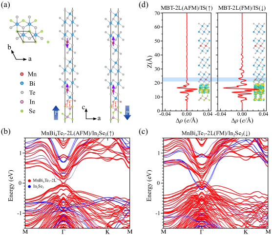
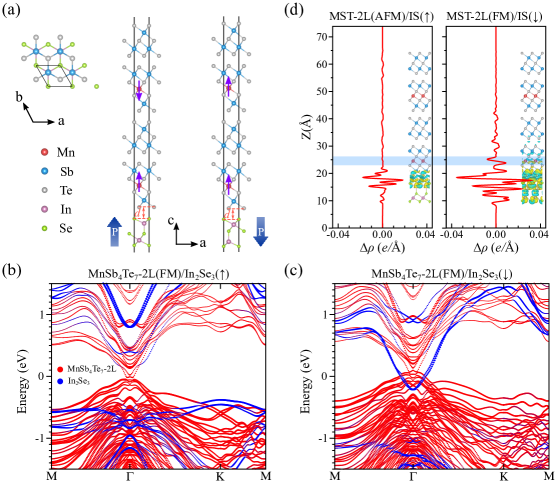
Figures S4-S6 show the geometric structures, layer-projected band structures, and differential charge density of MnSb2Te4-2L/In2Se3,
MnBi4Te7-2L/In2Se3, and MnSb4Te7-2L/In2Se3, respectively.
Similar to MnBi2Te4-2L/In2Se3 systems, the MAT-2L and FE In2Se3 monolayer with different polarization have a type-I and type-III band alignments.
For MAT-2L/In2Se3(), one
can see that charge transfer at the interface is negligible. Therefore, the IMCs remains to be AFM. In contrast, when the polarization flipping
to away from the interface, interlayer charge transfer becomes significant, which gives rise to hole doping to the Mn ions in the interfacial layer.
As a result, the FM state becomes energetically favorable.
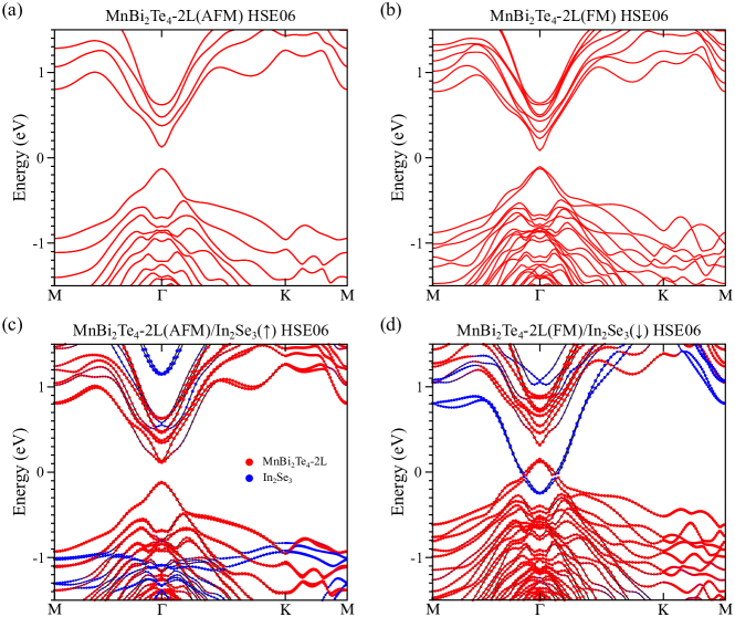
7. Band structure of freestanding MnBi2Te4-2L and MnBi2Te4-2L/In2Se3 with HSE06 method
Figure S7 displays the band structures of both freestanding MnBi2Te4-2L and MnBi2Te4-2L/In2Se3, which were computed using the HSE06 method with SOC. Fig S7(a) and (b) illustrate that the FM and AFM states of freestanding MnBi2Te4-2L have direct band gaps of around 186 and 252 meV, respectively. In contrast, the bandgap of 2L-MBT for FM and AFM IMCs was reduced to 170 and 236 meV when forming a heterojunction with In2Se3. Moreoever, Fig S7 further reveals that the HSE06 and PEB methods produced the same trend in terms of the switchable band alignment induced by monolayer FE In2Se3.
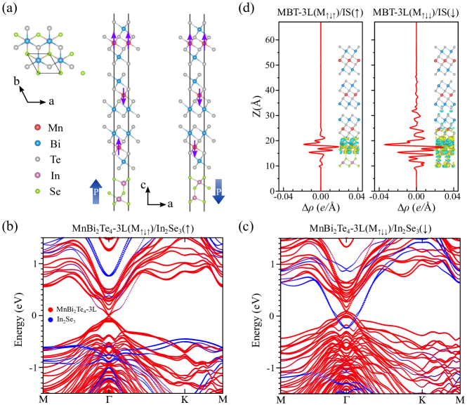
8. Interface effects on the electronic structure of MnBi2Te4 trilayers and quad-layers
Figures S8 and S10 show the geometric structures, layer-projected band structures, and differential charge density of MnBi2Te4-3L/In2Se3 and MnBi2Te4-4L/In2Se3, respectively. For the MnBi2Te4 trilayers and quad-layers systems, our calculations find that spin flipping is only taken place to the interfacial MnBi2Te4 layer. The results are similar to MnBi2Te4-2L/In2Se3.
9. Effects of substrates on the electronic structure and IMC of MnBi2Te4-2L/In2Se3
We considered nine different stacking configurations for h-BN/MnBi2Te4-2L/In2Se3/h-BN heterostructures. Fig. S10(a) shows the top and bottom views of the heterostructures, where only the three atomic layers at the interface (h-BN/Te-Bi or In-Se/h-BN) are presented. The energies are listed in Table. 4, which is referenced to the configuration of S1 with FM IMC and downward polarization. Overall, the h-BN substrate has little effect on the IMC in the heterojunction. The layer-projected band structures of h-BN/MnBi2Te4-2L/In2Se3/h-BN heterostructures withdifferent polarizations are shown in Fig. S10(c) and (d). The results demonstrate that the h-BN substrate does not alter the band arrangement between MnBi2Te4-2L and In2Se3, as it is a large bandgap insulator.
| Staking | h-BN/MnBi2Te4-2L/In2Se3()/h-BN | h-BN/MnBi2Te4-2L/In2Se3()/h-BN | ||||||
| FM | AFM | IMCs | FM | AFM | IMCs | |||
| S1 | 65.00 | 64.80 | 0.20 | AFM | 0.00 | 0.17 | -0.17 | FM |
| S2 | 70.16 | 69.93 | 0.23 | AFM | 5.04 | 5.19 | -0.15 | FM |
| S3 | 75.05 | 74.84 | 0.21 | AFM | 9.69 | 9.84 | -0.15 | FM |
| S4 | 68.15 | 67.92 | 0.23 | AFM | 3.54 | 3.71 | -0.17 | FM |
| S5 | 76.28 | 76.06 | 0.22 | AFM | 8.95 | 9.12 | -0.17 | FM |
| S6 | 78.00 | 77.78 | 0.22 | AFM | 12.37 | 12.53 | -0.16 | FM |
| S7 | 73.68 | 73.46 | 0.22 | AFM | 10.13 | 10.29 | -0.16 | FM |
| S8 | 78.43 | 78.21 | 0.22 | AFM | 15.15 | 15.30 | -0.15 | FM |
| S9 | 83.60 | 83.39 | 0.21 | AFM | 19.20 | 19.37 | -0.17 | FM |
10. Stability of different interlayer magnetic couplings in MnBi2Te4-based sandwiches
| IMC | freestanding | In2Se3()/MBT | In2Se3()/MBT | In2Se3()/MBT |
| -3L/In2Se3() | -3L/In2Se3() | -3L/In2Se3() | ||
| 0.47 | 0.17 | 0.00 | 0.17 | |
| 0.21 | 0.22 | 0.22 | 0.00 | |
| 0.00 | 0.06 | 0.41 | 0.07 | |
| 0.21 | 0.00 | 0.20 | 0.23 | |
| 0.47 | 0.17 | 0.00 | 0.17 | |
| 0.21 | 0.21 | 0.21 | 0.00 | |
| 0.00 | 0.06 | 0.42 | 0.08 | |
| 0.21 | 0.00 | 0.21 | 0.23 |
| IMC | freestanding | In2SSe2()/MBT | In2SSe2()/MBT | In2SSe2()/MBT | In2SSe2()/MBT |
| -4L/In2Se3() | -4L/In2Se3() | -4L/In2Se3() | -4L/In2Se3() | ||
| 0.70 | 0.40 | 0.12 | 0.39 | 0.70 | |
| 0.45 | 0.42 | 0.24 | 0.18 | 0.46 | |
| 0.21 | 0.24 | 0.11 | 0.00 | 0.21 | |
| 0.42 | 0.17 | 0.00 | 0.19 | 0.43 | |
| 0.21 | 0.00 | 0.07 | 0.24 | 0.21 | |
| 0.00 | 0.07 | 0.22 | 0.05 | 0.00 | |
| 0.22 | 0.21 | 0.35 | 0.20 | 0.21 | |
| 0.45 | 0.17 | 0.21 | 0.44 | 0.45 | |
| 0.70 | 0.40 | 0.12 | 0.38 | 0.70 | |
| 0.45 | 0.43 | 0.24 | 0.16 | 0.45 | |
| 0.21 | 0.24 | 0.11 | 0.00 | 0.21 | |
| 0.42 | 0.17 | 0.00 | 0.18 | 0.43 | |
| 0.21 | 0.00 | 0.09 | 0.25 | 0.21 | |
| 0.00 | 0.05 | 0.21 | 0.05 | 0.00 | |
| 0.22 | 0.22 | 0.31 | 0.21 | 0.21 | |
| 0.45 | 0.16 | 0.21 | 0.45 | 0.45 |
11. Kinetics pathways of ferroelectric transforming for MnBi2Te4-based heterojunctions
As discussed in the main text, sandwiching the MnA2Te4 thin films in between two different ferroelectric layers is a way of realizing the quadruple magnetic states. Here, we choose the ferroelectric monolayers of In2Se3 and In2SSe2 as substrates to tune the IMC of MAT films. Geometric structures of In2Se3 and In2SSe2 monolayers are shown in Fig. S11(a). The latter can be obtained by replacing the central Se atom of the former by a S atom. Figures S11 (c) and (d) show the kinetic pathways of ferroelectric transforming for MnBi2Te4-2L/In2Se3 and MnBi2Te4-2L/In2SSe2. Both systems has an asymmetric energy barriers due to the interface effect. For the MnBi2Te4-2L/In2Se3 (MnBi2Te4-2L/In2SSe2) system, the pathways of P()-to-P() and P()-to-P() has a barrier height are about 152 (245) and 220 (308) meV, respectively. The barrier heights of the MnBi2Te4-2L/In2SSe2 system are higher than those of the MnBi2Te4-2L/In2Se2. This trend is important in realizing the quadruplet magnetic state (see Fig.3 (c) in the main text).
Furthermore, we investigate the kinetic pathways for the transformings between the quadruple states in the In2SSe2/MnBi2Te4-4L/In2Se3 system by examining the barriers of all possible pathways. Fig. S12 shows a comparison of the energy barriers with respect to flip the polarization of In2Se3 and In2SSe2 layers. For the state with upward polarization for both the top and bottom ferroelectric layers, i.e., InSSe2()/MnBi2Te4-4L/In2Se3(), flipping the polarizations of InSSe2 layer has a barrier height that is about 154 meV higher than that the In2Se3 layer. Similarly, for InSSe2()/MnBi2Te4-4L/In2Se3() state, flipping the polarizations of InSSe2 layer has a barrier height that is about 23 meV higher than that of the In2Se3 layer. Therefore, the polarizations of In2Se3 have priority to those of the In2SSe2 to flip under external electric fields, which are desired for realizing quadruple magnetic states.
12. Topological properties of MnBi2Te4 thin films with different interlayer magnetic states
The topological properties of the MnBi2Te4 system are strongly related to the IMCs. Fig. S13 shows the IMCs dependence of edge states for freestanding MnBi2Te4 thin films. For the bilayer systems, we have gapped (gapless) edge states and 0 (1) for the Chen number () for the interlayer AFM (FM) ordering (see Figs. S13 a and b). For the trilayers, we obtain = 0, 1, and 0 for (), (), and (), respectively. As shown in Fig. S13 (c)-(e), the MnBi2Te4-3L in magnetic state () has gapless edge states in the bulk band gap, which are not seen for () and (). For MnBi2Te4 quad-layers, we obtain = 1, 0, -1, and 0 for (), (), (), and (), respectively. Correspondingly, () and () states have gapless edge states with opposite chiralities.
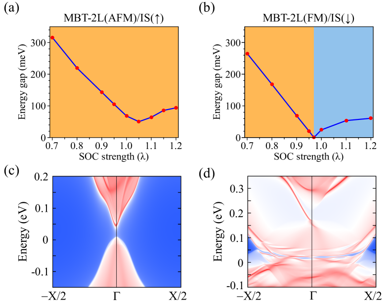
We expect that the ferroelectrically tunable Chern numbers can be seen in MnBi2Te4-based heterostructure. Fig. S14 shows the topological properties of MnBi2Te4-2L/In2Se3. For the bilayer systems, the topological properties of MnBi2Te4 remain unchanged upon interfacing, i.e., for the FM state and for the AFM state. The evolution of the band gap with respect to the SOC strength () is shown in Figs. S14(a) and (b). For the MnBi2Te4-2L(AFM)/In2Se3() state, the gap decreases with increasing and reaches a minimum (51 meV) at = 1.05. Then it increases as the SOC increases. However, for the MnBi2Te4-2L(FM)/In2Se3() state, the gap decreases and eventually closes at = 0.97 and then opens a gap with increasing , which shows a band inversion and topological phase transition. Furthermore, edge state calculations show that MnBi2Te4-2L(AFM)/In2Se3() state has no gapless states (Fig. S14c). Whereas MnBi2Te4-2L(FM)/In2Se3() state has a gapless edge state in the bulk energy gap (see Fig. S14d).