Determination of the ensemble transition dipole moments of self-assembled quantum dot films by time and angle resolved emission spectroscopy measurements
Abstract
The spontaneous emission of light in semiconductors is due to the excitonic relaxation process. The emission of light requires a change in the transition dipole matrix of the system. This is captured in terms of the physical quantity called transition dipole moment. The transition dipole moment (TDM) characterizes the line strength of the emission process. TDM is of fundamental importance in emitter-cavity interaction as its magnitude decides the interaction strength of emitters and cavities. In all light emitting devices, the orientation of the transition dipole moments is directly related to the optical power output of the devices. In this manuscript, the basic framework of spontaneous emission and Einstein coefficients is discussed for two level systems. Semiconducting alloyed quantum dots (AQDs) are synthesized in hydrophobic phase. AQDs are used as the experimental two level system. The AQDs are then self-assembled into monolayers by the Langmuir-Schaefer method. The ensemble averaged TDM magnitude and orientation of AQDs are extracted from the time resolved and the angle resolved emission spectroscopy measurements respectively. The procedure for finding out the TDM, described in this manuscript is generalized. The mentioned procedure can be extended to any emitters in hydrophobic phase.
I Introduction
Spontaneous emission process is at the heart of all light emitting devices (LEDs). Understanding the spontaneous emission process enables design of strategies and protocols for optimizing the light emission efficiencies of LEDs. According to the quantum theory of light, the spontaneous emission rate can be described in the terms of transition dipole moment () and the photonic density of states (PDOS) represented by . This is stated as the Fermi golden rule, which indicates the probability[1, 2] of a spontaneous emission rate between two energy levels E2 and E1 respectively is given as
The transition dipole moment[3] of two level system is given by
The Oscillator strength of the transition is defined as . The oscillator strength is directly related to the radiative decay lifetime and absorption cross-section of the two level system. Experimentally, it is convenient to measure radiative decay rate of a system, which can be expressed in terms of the Einstein A and B coefficients.[4]
The Einstein A and B coefficients describe the transition rate from the respective energy levels. A21 is the spontaneous emission rate from energy level 2 to energy level 1. B21 and B12 and are the absorption and stimulated emission rates of level 2 and 1 respectively.
The Einstein A and B coefficients are inter-dependent. The Einstein A coefficient is the reciprocal of the spontaneous emission life time (). The Einstein B coefficient is related to the absorption cross-section (). Both the coefficients are dependent on the transition dipole moment.
So to experimentally measure the transition dipole moment (TDM), either A21 or B21 have to be extracted from respective lifetime measurement or absorption cross-section measurement. The TDM magnitude can be extracted from either of the Einstein coefficients.
To extract the orientation of TDM, the angular dependence of the emission has to be measured. This can be done by two techniques. One technique is the back-focal plane (BFP) imaging[5] and the other is the angle resolved emission spectroscopy (ARES).[6, 7, 8, 9] BFP imaging is the preferred method for finding out the TDM orientation of single emitter. ARES is preferred for the ensemble measurement of TDMs of emitters.
By using either of these techniques, all the TDMs of the emitters are categorized into two orientations. One set of TDMs are oriented in the plane parallel to the substrate, denoted by . The other set of TDMs are oriented normal to the plane parallel to the substrate, denoted by . The ratio of the normally oriented TDMs to the total number TDMs is represented by parameter .
The parameter is called anisotropy coefficient and its values range from 0 to 1. For an isotropic emitter the value of is 0.333. If an emitter TDM is completely oriented out of the substrate plane, the value of is 1. If the value of is zero, then the emitter TDM is completely oriented in the plane of the substrate. As the emission intensity is directly proportional to the number of emitters, the measurement of the intensity of both the emitters in the plane and out of plane can give the value of the anisotropy coefficient. The measurement of one of the Einstein coefficients and the anisotropy coefficient gives the magnitude and direction of TDMs.
It has been demonstrated that the display devices and LEDs have optimal emission efficiency and output optical power, when the TDMs of the emitters are oriented in the plane of substrate.[10, 11] Due to the above mentioned considerations, determination of TDMs of emitters is of use to the LED and display industry.
Also from the perspective of controlling the interaction of emitters with a cavity, the knowledge of orientation is needed. If the cavity mode field () interacts with N emitters, the coupling coefficient (g)[12, 13, 14] is given by
By choosing optimally oriented TDMs () with appropriate concentration (N), the coupling (g) with cavity can be controlled.
This report describes the procedure of synthesis, characterization transfer of monolayers of AQDs in hydrophobic phase to a substrate. Experimental methods used for extraction of TDM magnitude and orientation are discussed. Details of the angle resolved emission spectroscopy instrumentation is also included. The spectroscopic procedures are generalized and can be used for determination of TDMs of nanosized emitters in hydrophobic phase as CdSe rings[15] and CdSe platelets.[16]
II Experimental Methods
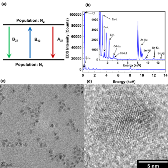
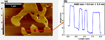
The AQDs used in this study are synthesized by one-pot hot injection method.(Appendix A) The synthesized AQDs are characterized by transmission electron microscopy (TEM) and atomic force microscopy (AFM) as shown in Fig. 1, Fig. 2 and Fig. 3. The AQD size is extracted from AFM height profile in Fig. 2. The mean size of AQDs is 5.6 nm 0.3 nm. TEM images are not considered for size estimation due to Argon plasma treatment done to AQDs before the TEM measurement.(Appendix B) The TEM and energy dispersive spectroscopy (EDS) measurements are performed with a Titan Themis 300 kV TEM instrument.
The AQDs are self-assembled in to monolayers by Langmuir Schaefer method.(Appendix C) The energy dispersive spectra of AQDs is measured for composition determination. The synthesized AQDs emission is in visible region of light. So, the spontaneous emission process is Photoluminescence (PL). The steady state photoluminescence (PL) and time resolved photoluminescence (TRPL) are measured for the 5ML sample using a confocal microscope.(Witec alpha 300). 532 nm continuous wave (CW) laser and 405 nm pulsed lasers are focused onto the sample in reflection geometry using fiber coupled beam splitter and 20X magnification objective with numerical aperture (NA) 0.22. For PL measurement the 532 nm laser diode output power is set at 10 W and the reflected light is filtered through a 532 nm edge notch filter to reject laser line. The filtered light is then relayed onto a 600 grooves/mm grating coupled Peltier cooled CCD detector. The CCD integration time is set at 5s and averaged over 4 accumulation cycles. The PL intensity is measured in arbitrary units. (a.u.) For TRPL measurement, the pulsed laser repetition rate is set at 20 MHz, which translates to 50 ns temporal separation between two consecutive pulses. The emitted light is collected with 20X/0.22 NA objective and filtered from the probing laser pulses using a 488 nm long pass filter. The integration time is 10 s and the emission is averaged over 10 accumulation cycles. The TRPL is measured by time correlated single photon counting (TCSPC) method[17] using a Picoquant SPAD detector.
III Spectroscopic Properties of Self-assembled AQD Layers
III.1 Steady State and Time Resolved Photoluminescence Measurements
The steady state PL measurement is averaged over the objective focused spot. The objective spot size (d) is diffraction limited.[18] It is given by . The value of d for CW 532 nm laser is 2.95 m and it is 2.25 m for 405 nm pulsed laser. So, the steady state PL spectra and TRPL measurements averages about 105 AQDs. The measured spectra are shown in Fig. 4.
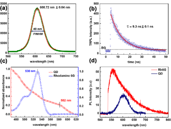
The PL emission spectra is fitted with a Gaussian function and the peak position is at 608.71 nm 0.04 nm. The PL spectral line width is given by the Gaussian’s full width half maximum (FWHM). The FWHM of 5 AQD layers is 39.72 nm 0.11 nm. The PL decay curve is fitted with a single exponent decay function, to account the single decay channel available to the AQD layers i.e., decay into free space. The decay lifetime 5 AQD layers is 9.3 ns 0.1 ns. The measured PL peak position () is taken as 608.71 nm and the Einstein coefficient A21 is taken as reciprocal of = 9.3 ns. Considering speed of light c =2.998x10⁸ m/s, the angular frequency () of the QD PL transition is given by
The TDM magnitude can be calculated from equation (3) as follows
Generally the TDM values are reported in Debye units instead of SI units. Converting to debye units as, 1D = 3.335x10⁻³⁰ C-m, the value of AQD ensemble average TDM turns out as =1.003 D 0.005 D. The extracted values agrees with the order of reported[19] oscillator strength of , which gives TDM magnitude as D for CdSe quantum dots. The Einstein coefficient A21 and B12 are given as
The value of A21 is estimated to be 0.11 ns-1 0.01 ns-1. The value of B21 can be estimated from equation (10) by using value of A21.
III.2 Quantum Yield Determination
The PL quantum yield () of the AQDs is measured by the relative optical method.[20] In this method a fluorescent dye with known quantum yield is chosen as an standard sample. The emission and absorption spectrum of dye and quantum dots are measured. The quantum yield of QDs can be measured relative to the dye as
The Rhodamine 6g (Rh6G) dye is chosen as standard dye sample, as its quantum yield is 0.75 in Chloroform solvent at concentrations lower than 10-5 M i.e. 12 g ml-1.[21] 1 mgml-1 AQD solution and 6.7 gml-1 Rh6G solution are prepared in Chloroform solvent. The solution is then spin coated on a glass slide at 3000 rpm and for 60s. The corresponding background corrected PL spectra are shown in Fig. 10. The spectra are integrated to calculate the spectral integrated PL factor given by
The integration is carried from 532 nm till the intensity reaches zero for AQDs and Rh6G. The absorption factor () is given by
Here is the specific absorbance, c is the concentration and l=1 cm is the length of cuvette used for measurement. The absorbance of the solutions is measured in a Perkin Elmer -35 UV-VIS spectrometer. Absorbance of solutions with three different concentration of both Rh6G dye and AQDs are measured and the values are shown in Table I.
| Emitter | Specific Absorbance () | Concentration (c) |
|---|---|---|
| AQD | 0.0828 mg-1ml cm-1 | 1 mgml-1 |
| Rh6g | 0.2608 g-1ml cm-1 | 6.7 g/ml |
The spectral integrated PL factor for Rh6G and AQDs is 4245.32 a.u and 916.72 a.u. Plugging in the and factors in equation (11) and with =0.75, the value of AQD quantum yield turns out as 0.61 0.01. The typical reported[22] values of AQD quantum efficiency range from 0.6 to 0.8. AQDs are preferred over core-shell quantum dots, as the lattice mismatch in AQD is minimal due to composition gradient. The minimal lattice mismatch improves the quantum yield.[23]
III.3 ARES setup
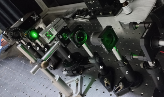
ARES system is assembled in our lab, for determining ensemble TDM orientation of emitters in transmission mode as shown in Fig. 5. The refined ARES design[24] was used for assembly of the spectroscopic system. The details of the optical components used in this setup are mentioned in table. II.
| Marker | Catalogue number | Description | Manufacturer |
|---|---|---|---|
| 1 | CPS532 | DPSS laser | Thorlabs |
| 2 | LB1676-ML | bi-convex lens | Thorlabs |
| N | ND06A/ND03A | ND filters | Thorlabs |
| 3 | P1000K | pinhole | Thorlabs |
| 4 | PR01 | rotation stage | Thorlabs |
| 5 | AL2550M-A | aspheric lens | Thorlabs |
| 6 | FELH0550 | long pass filter | Thorlabs |
| 7 | WP25M-VIS | linear polarizer | Thorlabs |
| 8 | PAF2S-11A | aspheric fiberport | Thorlabs |
| 9 | QE-Pro | CCD | Ocean optics |
| F | QP600-2-UV-VIS | optical fiber | Ocean optics |
532 nm diode pumped solid state (DPSS) laser module rated at 4.5 mW is used for exciting Photoluminescence spectra from the AQDs. The laser beam path is aligned parallel to the optical table by using two 1 mm pin holes set at same height from the surface of optical table. Once the alignment is complete, the optical axis of the components is set by the laser beam path.
Then a bi-convex lens of focal length 100 mm is placed before the laser diode so that the pinhole and laser are on the both foci of the lens. Then a BK-7 glass half cylinder of radius 20 mm is placed on a rotating stage. The rotation axis of the stage is aligned with the cylinder symmetry axis. The laser beam spot size on the cylinder is about 3 mm.
An aspheric lens and an aspheric fiberport is set at 110 mm and 310 mm from the cylinder axis respectively. One end of an optical fiber is inserted inside the fiberport and the other end is inserted into a Peltier cooled CCD spectrometer input port. A 550 nm long pass filter and a linear polarizer is placed between the aspheric lens and fiber port.
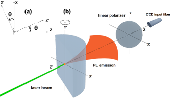
For ARES measurement, three different concentrations have been selected. Three 18 mm x 18 mm glass coverslips are sonicated in Acetone and Isopropyl alcohol for 5 minutes and dried under nitrogen flow. 1 mg/ml solution of AQDs is prepared in n-hexane. 50 L of the AQD solution is spin coated (SC) on to one cover slip for two cycles at 3000 rpm and 60s. 3 monolayers (3ML) and 5 monolayers (5ML) of AQDs are transferred onto coverslips by LS method. The samples are denoted by SC, 3ML and 5ML respectively. The cover-slide is stuck on a BK-7 half-glass cylinder (nglass=1.520) using a single drop of Leica index matching oil (noil=1.518). Essentially the refractive index is uniform till the emitted light from the spot on the glass substrate reaches the cylindrical surface. Light does not undergo refraction at the cylindrical surface and the emission pattern of film is directly mapped out. The emission pattern is focused into the fiber port by the aspheric lenses. The 550 nm long pass filter, in the between the aspheric lenses filters out the laser line.
The linear polarizer plate is used to select the emission polarized along the along horizontal and vertical axes relative to the optical table plane, as shown in Fig. 6. As the light emitted by the dipoles is polarized along the TDM direction, the horizontal and vertical polarized emission intensity represents the dipoles oriented along the horizontal and vertical axes. By rotating the half cylinder, the polarised PL emission spectra of the AQDs deposited on the glass slide can be measured. The PL emission intensity of the AQDs measured without the polarizer plate in beam path, represent the emission due to all the dipoles in the incident laser beam spot.
From the angle dependence of these three spectral measurements, TDM orientation can be estimated from the anisotropy coefficient as
Here is the anisotropy parameter. represents the intensity of dipoles normal to the substrate. represents the intensity of dipoles parallel to the substrate. Io is the measured unpolarized intensity. To avoid the wavelength dependence, wavelength integrated PL spectra are used.
III.4 Orientation of Transition Dipole Moments of Self-Assembled Alloyed Quantum Dot Layers
The angle dependent PL emission spectra are measured by placing a linear polarizer plate in the beam path before the CCD input fiber. The polarizer (WP25M-VIS) has an average extinction rate of 800:1. The polarization axis of the linear polarizer can be rotated to align with horizontal and vertical directions. The vertical and horizontal axes are denoted by Y and X axes. The laser beam line is considered parallel to the Z axis.
The far field intensity (I) of a point dipole is given by the magnitude of time averaged Poynting vector (),[25, 26] as
So, the intensity radiated by an ensemble of dipoles can be summed in terms of the intensities radiated by the individual dipoles along X, Y and Z axes.
The substrate is assigned a co-ordinate system (X’, Y’ and Z’) fixed with the laser beam spot center as origin. The angle dependence of polarized PL emission along X and Y axes is measured. The polarizer plate is removed and then the unpolarized angle dependent PL emission is measured. The polarized emission along Z axis can be extracted by subtracting the net polarized PL emission from the unpolarized PL emission.
The glass cylinder is rotated along the Y’=Y axis, which coincides with the symmetry axis of the glass cylinder. To extract the intensity from the TDMs along axes (X’,Y’ and Z’) from the measured emitted intensity of TDMs along X, Y and Z axes. By ignoring the transmission losses, this can be done by a rotation of axes, by angle around Y axis.
Considering the substrate plane is defined as X’-Y’ plane, the in plane () and out of plane () contributions can be expressed as
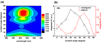
The fitted spectral map for the data measured by ARES setup is shown in Fig. 7(a) for 5ML sample. For 5ML sample, the full width half maximum (FWHM) of PL spectra is considered for further analysis. The polarization dependent PL spectra at each incident angle is obtained by integration over the FWHM.
The cylinder axis was deliberately misaligned with laser beam, by shifting the cylinder along X axis about 3 mm, in order to visualize the effect on angle resolved emission. The raw angle resolved emission pattern for misaligned and aligned system are compared in Fig. 7(b). For the misaligned system, the contrast between angles is poor and emission pattern is spread over the angles. In case of the aligned system, the emission pattern contrast is sharp.
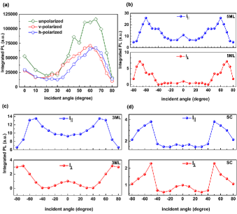
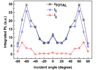
The corresponding integrated spectral data is shown in Fig. 8(a) for 5ML sample.The data is only collected from 0o to 80o. For better visibility the data is duplicated till -80o. The intensity contribution of in the plane (IP) and out of plane (OP) dipoles is extracted from the data using the equations (16-20). The processed data is shown in Fig. 8(b), which encapsulates the far field emission pattern of ensemble of AQDs. Similarly the processed data is shown in Fig. 8(c) and Fig. 8 (d) for 3ML and SC samples. From the IP and OP emission patterns,the anisotropy parameter is extracted by using equation (14).
A single CdSe-ZnS or CdSe quantum dot has a circular TDM due to the two fold degeneracy in the exciton states.[27, 28]. In an ensemble, due to the averaging over 1011 dots, the TDM becomes isotropic. AQD ensemble PL emission is reported as isotropic.[29] The AQD 5ML sample also serves as a benchmark for the ARES instrument.
The anisotropy coefficient represents the ratio of out of plane TDMs to the total TDMs in the beam spot. With the value of , the orientation of TDM can be known. The mean anisotropy coefficient measured for the AQDs is mentioned in the table. III. The worst case anisotropy coefficient measured for 5ML AQD sample is 0.351, which amounts to a 6% deviation from the expected value 0.333. The value agrees with the reported range of anisotropy coefficient for CdSe-CdS quantum dots is 0.33 to 0.35.[24]
The OP and IP contributions are extracted from the IP () and OP () intensities to the total intensity (). The ARES measurement affirms that the OP dipole contribution is minimal at normal incidence and it is significant at oblique incidence. So most of the light emitted at angles 40o can be attributed to IP transition dipoles.
| Sample | |
|---|---|
| SC | 0.430 0.002 |
| 3ML | 0.291 0.002 |
| 5ML | 0.349 0.002 |
The angular emission emission pattern changes significantly with the increasing AQD layers, i.e. concentration of AQDs. The intensity contrast between near normal and oblique angles increases from SC to 3ML and is largest for 5ML sample. The agreement of the anisotropy coefficient, with ideally expected value also improves in a similar trend.
So this indicates that if the emitter quantum yield is less than 60 %, then then multiple layers of emitters are to be deposited on the substrate, to get an accurate angle resolved emission pattern. If the emitter quantum yield is near unity,[30] for example in the case of CdSe/CdS quantum dots, even spin-coated substrate can give an accurate angle resolved emission pattern.[24]
| Sample | angle | IP (%) | OP (%) |
|---|---|---|---|
| SC | 0o | 39 | 61 |
| SC | 70o | 33 | 67 |
| 3ML | 0o | 90 | 10 |
| 3ML | 70o | 73 | 27 |
| 5ML | 0o | 92 | 8 |
| 5ML | 70o | 65 | 35 |
The IP and OP contributions in Table IV, from the SC sample deviate significantly from the monolayer samples (3L and 5L). This can be understood from the poor intensity contrast at normal incidence for SC sample. The agreement between 3L and 5L samples is good. Essentially the IP dipole emission is dominantly detected at normal incidence and the OP dipoles emission is dominantly detected at angles larger than 70o.
IV Conclusion
The synthesized AQDs are characterised by TEM and AFM and have a quantum yield of the AQDs is 60%. Ensemble PL and TRPL measurements indicate a TDM value of 1 D for the AQDs. The PL emission of the ensemble is isotropic as the orientation of TDMs is distributed equally in all directions. The in the plane dipole contribution to PL emission is dominant at normal incidence and the out of plane dipole contribution to the PL emission is dominant at oblique angles of incidence. This manuscript lays out the procedure for measuring TDM magnitude and orientation of an ensemble of any emitters in hydrophobic phase.
Acknowledgements.
Authors acknowledge the use of many mechanical components of the angle resolved emission spectroscopy (ARES) setup from late Prof. Vasant Natarajan’s lab, Physics department, Indian institute of science (IISc), Bengaluru. Authors acknowledge financial support from science & engineering research board (SERB), India and institute of eminence (IoE) grant from the Ministry of human resource development (MHRD) executed through IISc. B. Tongbram thanks the Department of science and technology (DST), Inspire faculty programme for fellowship. H.R. Kalluru thanks the Micro and nano characterization facility (MNCF-CeNSE), IISc for access to titan themis 300 kV TEM facility.Appendix A Alloyed Quantum Dot Synthesis
For use as emitters in this study alloyed quantum dots (AQDs) are synthesized. The reported[31, 32] hot injection procedure is used for synthesizing AQDs. The glassware used for synthesis is cleaned in hot RCA SC-I solution[33] for 10 minutes. Then the glassware is cleaned in an ultrasound bath and subsequently rinsed thrice with ultra-pure DI water and dried in an oven.
Cadmium oxide powder (CdO-99.5%), Zinc Oxide powder (ZnO-99%), Oleic Acid (OA-90%), Selenium powder (Se-99.99%), Sulphur powder (S-99.9%) Trioctyl phosphine (TOP-99%) n-Hexane (99%) and Octadecene (ODE-99%) are procured from Merck.
25.68 mg CdO, 162.81 mg ZnO, 3.52 ml OA and 10ml ODE are measured and dropped in a three-neck borosilicate glass flask of volume 50 ml, along with a Teflon magnetic stirrer bead. 21 mg Se powder, 84.6 mg S powder and 2 ml TOP is added in a borosilicate glass vial. The glass vial with Se-S-TOP precursors is flushed with Nitrogen gas and sonicated in an ultrasound bath for twenty minutes till the solution becomes completely transparent.
The three-neck flask is placed on a magnetic stirrer plate in a heating mantle with a PID controller and temperature feedback sensor. The flask is then connected to a condenser column, which is connected to a Schlenk line, with a dual passage option for flushing the flask with gas and evacuating the flask. The flask necks are closed with rubber septa and sealed with Teflon tape to avoid air leakage into the flask. The flask is then evacuated with a turbo pump through the Schlenk line and the vacuum is maintained for 30 minutes, with the help of a vacuum pump. Then the PID is turned on with a set temperature C. The solution in flask is heated to the set temperature under vacuum. Then the flask is held at set temperature for 30 minutes under vacuum.
Then the vacuum pump is turned off and the flask is flushed with Nitrogen gas and flow of nitrogen gas is maintained throughout the synthesis. As Nitrogen gas is heavier than air it settles in bottom half of the three-neck flask and forms a barrier against any atmospheric oxygen leaking in. The whole heating mantle is wrapped in glass-wool to insulate the flask and prevent loss of heat due to thermal radiation. The solution is flask should be pale yellow in colour. Now the set temperature of PID is changed to C. As soon as the temperature reaches C, 1.5 ml of Se-S-TOP solution is injected into the flask with help of a syringe and pipette.
The reaction mixture rapidly turns orange and then dark red. The reaction is allowed to proceed for 15 minutes from injection time. The solution temperature is maintained at 305o C 5 o C for the duration. Then the PID is turned off and the flask is quenched in a water bath to stop the reaction. As the reaction mixture reaches room temperature, 15 ml of Acetone (99%) and 5 ml Chloroform (99.9%) is added to reaction mixture. The leftover precursors dissolve in the Acetone phase. The AQDs dissolve in the Chloroform phase and get separated from the precursors. This reaction mixture is further cleaned by centrifuging.
After centrifuging for 10 minutes at 12000 rpm, the precipitate is collected and re-dispersed in 3 ml Chloroform. The supernatant solution is discarded in a glass bottle. Then 9 ml Acetone is added to chloroform solution. This completes one cycle of cleaning. Two more such cycles are repeated. The precipitate is selected and the supernatant is discarded in every cycle. The precipitate after third cycle is dispersed in chloroform and allowed to dry out in a desiccator. The AQD powder is stored in a cleaned glass vial in dark for further use.
Appendix B Structural composition of AQDs
The synthesized AQDs are characterized by transmission electron microscopy (TEM) and energy dispersive X-ray spectroscopy (EDS) measurements, by using a Thermofisher titan themis 300 kV TEM machine. 10 g/ml AQD solution is prepared and is dropcasted on to a copper TEM grid and allowed to dry under ambient conditions. Then the grid is placed under vacuum for 24 hours. Before mounting onto TEM machine, the TEM grids are cleaned under Argon plasma for 40 seconds at 23 W power and 4.7x10⁻² torr pressure to minimize the organic residues due to oleic acid ligands and hexane solvent. This is also essential to maintain vacuum, as the residual organic molecules on the TEM grid i.e., oleic acid and hexane, degass under electron beam. So Argon plasma cleaning changes the size of AQDs. The AFM imaging gives a more reliable mean value of the size of AQDs compared to TEM imaging.
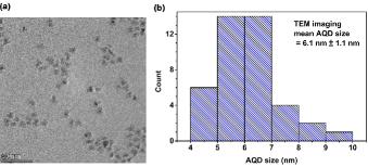
The analysis of the TEM images indicate that the mean AQD size is 6.1 nm 1.1 nm. The size estimate is poor relative to the AQD size estimate from AFM image. The AFM image height profile indicates mean AQD size as 5.6 nm 0.3 nm, which is a better way to estimate AQD size.
EDS is a semi-quantitative tool used to analyse the chemical composition of alloys.[34, 35] The EDS spectra of the AQDs have the characteristic X-rays of Cadmium, Selenium, Zinc and Sulphur. The large carbon mass fraction is attributed to the organic ligand and solvent. The relative atomic fractions of the pairs (Cd:Se) and (Zn:S) are 1.1 0.2 and 1.06 0.2. This indicates that the dot composition is near uniform as x= 0.52 0.1 and y= 0.51 0.1. The EDS analysis shows that Cd, Se, Zn and S atomic ratios are nearly equal.
| Element | Atomic fraction (%) | Error (%) |
|---|---|---|
| Carbon | 98.42 | 1.95 |
| Sulphur | 0.66 | 0.12 |
| Zinc | 0.7 | 0.09 |
| Selenium | 0.10 | 0.01 |
| Cadmium | 0.11 | 0.01 |
Appendix C AQD Self-assembled Monolayers
Monolayers of AQDs are fabricated by self-assembly via langmuir-schaefer (LS) method. The LS method is a versatile method used to transfer monolayers of colloidal quantum dots with hydrophobic ligands on to substrates as silicon, glass and quartz.[36, 37] The LS setup consists of a Teflon trough coated with a hydrophobic coating. Similar hydrophobic Teflon barriers are placed on the trough and ultra-pure deionised (DI) water (resistivity-18.2 M) from a DI water system (Millipore) is filled in the trough till a water meniscus forms between the barriers. A pressure sensor is placed in between the barriers to sense the changes in surface pressure. 1.2 mg/ml AQD solution in n-Hexane is centrifuged for a fourth cycle, at 12000 rpm for 10 minutes. The supernatant solution is separated from the precipitate and is dispersed drop-wise using a Hamilton micro-syringe (50 L capacity) between the barriers. Typically, 100 L of AQD solution is used for a single monolayer transfer.
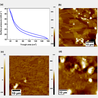
Once the AQD solution is dispersed, then the barriers are brought together using a stepper motor at a speed of 10 mm/min. This results in raising surface pressure, as the AQD are hydrophobic and compression of area between barriers results in mutual repulsive forces. If the AQDs are packed till monolayer limit, then further packing is not possible and as a result the surface pressure saturates. This indicates the formation of monolayer via self-assembly. At this point the substrate is lowered onto the area between barriers, by a motorised dipper at a rate of 10 mm/min. The substrate is allowed to touch the water surface and then is retracted at the same speed. The monolayer is now transferred onto the substrate.
The barrier compression speed and number of isothermal compression and relaxation cycles executed before the transfer determines the compactness of the monolayer. Due to rapid barrier compression speed, large lateral monolayers cannot form, as compact self-assembly needs time for compact packing. Also multiple isotherms will seal the gaps between self-assembled monolayer domains. This has been verified by atomic force microscope (AFM) imaging of the monolayers. The non-contact mode AFM is used for measurement, as it can measure precisely sub-nm range features of the sample.[38]
Silicon wafers are ultrasonically cleaned in Acetone, then subsequently in Isopropyl alcohol and then dried in Nitrogen gas flow. These wafers are used as substrate for transfer of monolayers and AFM imaging. A monolayer is transferred onto Silicon substrate after 3 compression cycles at 25 mm/min barrier speed and surface pressure of 35 mNm-1. NC-AFM images for the sample indicate that the monolayers are laterally small in size and are about 500 nm.
Compact monolayer can be transferred on silicon substrates, only after 10 compression cycles and at barrier compression speed of 10 mm/min. Sequentially, 3 and 5 monolayers are transferred sequentially onto silicon wafers, after 10 compression cycles and at barrier compression speed of 10 mm/min and surface pressure of 42 mNm-1. For all the three samples, the topography is imaged by AFM. The AFM imaging indicates that at least 10 cycles of compression are necessary for a compact monolayer, with large lateral dimensions. The substrate is wholly covered in case of 5 sequential monolayers. Considering CdSe/ZnS QDs aggregate in a hexagonal close packed structure at air-water interface,[39] the maximum packing fraction is 74%.[40] The area of 1 mm2 on the substrate, only 0.74 mm2 is filled by AQDs and each quantum dot is considered to be spherical in shape with 6 nm diameter. This translates to 3x10¹⁰ AQDs per monolayer per mm circular spot. For 5 monolayers, the density is 1.5x10¹¹ per mm. So, the estimated order of emitters in a mm spot is 1011.
References
- Loudon [2000] R. Loudon, The Quantum Theory of Light (Oxford University Press, New York, 2000).
- Scully and Zubairy [1997] M. O. Scully and M. S. Zubairy, Atom–field interaction – quantum theory, in Quantum Optics (Cambridge University Press, 1997) p. 193–219.
- Ditchburn [1976] R. Ditchburn, Light, Light No. v. 1 (Academic Press, 1976).
- Hilborn [1982] R. C. Hilborn, Am. J. Phys. 50, 982 (1982).
- Kim et al. [2020] J. Kim, H. Zhao, S. Hou, M. Khatoniar, V. Menon, and S. R. Forrest, Phys. Rev. Applied 14, 034048 (2020).
- Ohta and Fujieda [2017] M. Ohta and I. Fujieda, in Frontiers in Optics 2017 (Optica Publishing Group, 2017) p. JTu2A.1.
- Fujieda and Ohta [2017] I. Fujieda and M. Ohta, AIP Advances 7, 105223 (2017).
- Frischeisen et al. [2010] J. Frischeisen, D. Yokoyama, C. Adachi, and W. Brütting, Appl. Phys. Lett. 96, 073302 (2010).
- Graf et al. [2014] A. Graf, P. Liehm, C. Murawski, S. Hofmann, K. Leo, and M. C. Gather, J. Mater. Chem. C 2, 10298 (2014).
- Furno et al. [2012] M. Furno, R. Meerheim, S. Hofmann, B. Lüssem, and K. Leo, Phys. Rev. B 85, 115205 (2012).
- Fuchs et al. [2015] C. Fuchs, P.-A. Will, M. Wieczorek, M. C. Gather, S. Hofmann, S. Reineke, K. Leo, and R. Scholz, Phys. Rev. B 92, 245306 (2015).
- Törmä and Barnes [2014] P. Törmä and W. L. Barnes, Rep. Prog. Phys. 78, 013901 (2014).
- Khitrova et al. [2006] G. Khitrova, H. M. Gibbs, M. Kira, S. W. Koch, and A. Scherer, Nat. Phys. 2, 81 (2006).
- Kalluru and Basu [2022] H. R. Kalluru and J. K. Basu, Phys. Rev. Appl. 18, 014004 (2022).
- Hartmann et al. [2019] N. F. Hartmann, M. Otten, I. Fedin, D. Talapin, M. Cygorek, P. Hawrylak, M. Korkusinski, S. Gray, A. Hartschuh, and X. Ma, Nat. Commun. 10, 3253 (2019).
- Scott et al. [2017] R. Scott, J. Heckmann, A. V. Prudnikau, A. Antanovich, A. Mikhailov, N. Owschimikow, M. Artemyev, J. I. Climente, U. Woggon, N. B. Grosse, and A. W. Achtstein, Nat. Nanotechnol. 12, 1155 (2017).
- O’Connor and Phillips [1984] D. V. O’Connor and D. Phillips, in Time-Correlated Single Photon Counting (Academic Press, 1984) pp. 36–54.
- Hecht [2017] E. Hecht, Optics, Fifth Edition (Pearson Education Limited, England, 2017).
- Leistikow et al. [2009] M. D. Leistikow, J. Johansen, A. J. Kettelarij, P. Lodahl, and W. L. Vos, Phys. Rev. B 79, 045301 (2009).
- Grabolle et al. [2009] M. Grabolle, M. Spieles, V. Lesnyak, N. Gaponik, A. Eychmüller, and U. Resch-Genger, Anal. Chem. 81, 6285 (2009).
- Reisfeld et al. [1988] R. Reisfeld, R. Zusman, Y. Cohen, and M. Eyal, Chem. Phys. Lett. 147, 142 (1988).
- Bae et al. [2008] W. K. Bae, K. Char, H. Hur, and S. Lee, Chem. Mater. 20, 531 (2008).
- Reiss et al. [2009] P. Reiss, M. Protière, and L. Li, Small 5, 154 (2009).
- Hänisch et al. [2020] C. Hänisch, S. Lenk, and S. Reineke, Phys. Rev. Applied 14, 064036 (2020).
- Luan et al. [2006] L. Luan, P. R. Sievert, and J. B. Ketterson, New J. Phys. 8, 264 (2006).
- Jackson [1998] J. D. Jackson, Classical Electrodynamics, 3rd Edition (JOHN WILEY & SONS, INC, 1998).
- Brokmann et al. [2004] X. Brokmann, L. Coolen, M. Dahan, and J. P. Hermier, Phys. Rev. Lett. 93, 107403 (2004).
- Chung et al. [2003] I. Chung, K. T. Shimizu, and M. G. Bawendi, Proc. Natl. Acad. Sci. U.S.A. 100, 405 (2003).
- Yadav et al. [2020] R. K. Yadav, W. Liu, S. R. K. C. Indukuri, A. B. Vasista, G. V. P. Kumar, G. S. Agarwal, and J. K. Basu, J. Condens. Matter Phys. 33, 015701 (2020).
- Greytak et al. [2012] A. B. Greytak, P. M. Allen, W. Liu, J. Zhao, E. R. Young, Z. Popović, B. J. Walker, D. G. Nocera, and M. G. Bawendi, Chem. Sci. 3, 2028 (2012).
- Győri et al. [2015] Z. Győri, Z. Kónya, and Á. Kukovecz, React. Kinet. Mech. Catal. 115, 129 (2015).
- Nag et al. [2008] A. Nag, A. Kumar, P. P. Kiran, S. Chakraborty, G. R. Kumar, and D. D. Sarma, J. Phys. Chem. C. 112, 8229 (2008).
- Celler [1999] G. K. Celler, Electrochem. solid-state lett. 3, 47 (1999).
- Newbury and Ritchie [2013] D. E. Newbury and N. W. M. Ritchie, Scanning 35, 141 (2013).
- Del Angel et al. [1989] G. Del Angel, S. Alerasool, J. Domínguez, R. Gonzalez, and R. Gómez, Surf. Sci. 224, 407 (1989).
- Lambert et al. [2010] K. Lambert, R. K. Čapek, M. I. Bodnarchuk, M. V. Kovalenko, D. Van Thourhout, W. Heiss, and Z. Hens, Langmuir 26, 7732 (2010).
- Parchine et al. [2016] M. Parchine, J. McGrath, M. Bardosova, and M. E. Pemble, Langmuir 32, 5862 (2016).
- Hapala et al. [2015] P. Hapala, M. Ondráček, O. Stetsovych, M. Švec, and P. Jelínek, Simultaneous nc-afm/stm measurements with atomic resolution, in Noncontact Atomic Force Microscopy: Volume 3, edited by S. Morita, F. J. Giessibl, E. Meyer, and R. Wiesendanger (Springer International Publishing, Cham, 2015) pp. 29–49.
- Crawford and Leblanc [2014] N. F. Crawford and R. M. Leblanc, Coord. Chem. Rev. 263-264, 13 (2014), quantum Dots.
- Ashcroft and Mermin [1976] N. W. Ashcroft and N. D. Mermin, Solid State Physics (Holt, Rinehart and Winston, New York, 1976).