The topological magnetoelectric effect in semiconductor nanostructures:
quantum wells, wires, dots and rings
Abstract
Electrostatic charges placed near the interface between ordinary and topological insulators induce magnetic fields, through the so-called topological magnetoelectric effect. Here, we present a numerical implementation of the associated Maxwell equations. The resulting model is simple, fast and quantitatively as accurate as the image charge method, but with the advantage of providing easy access to elaborate geometries when pursuing specific effects. The model is used to study how magnetoelectric fields are influenced by the dimensions and the shape of the most common semiconductor nanostructures: quantum wells, quantum wires, quantum dots and quantum rings. Point-like charges give rise to magnetic fields of the order of mT, whose sign and spatial orientation is governed by the geometry of the nanostructure and the location of the charge. The results are rationalized in terms of the Hall currents induced on the surface, which constitute a simple yet valid framework for the deterministic design of magnetoelectric fields.
I Introduction
Early works introducing axion electrodynamics in quantum field theory noticed that the ordinary Maxwell equations had to be complemented with additional terms, whereby static electric fields would induce magnetic polarization and, in turn, static magnetic fields would induce charge polarization.Wilczek (1987) This phenomenon, known as the magnetoelectric effect, has been later on predicted and observed in a number of condensed matter systems.Nenno et al. (2020); Yīng and Zülicke (2022) One such system are topological insulators (TI).Bernevig et al. (2006); Qi and Zhang (2011) Here, the magnetoelectric polarizability –responsible for the coupling of magnetic and electric fields– is isotropic and takes quantized values in terms of the fine structure constant.Maciejko et al. (2010); Vazifeh and Franz (2010) This is in contrast to ordinary insulators (OI), where the polarizability is zero. Experimental verifications of this effect have been recently reported in TI materials such as thin films of Crx(Bi0.26Sb0.74)2-xTe3Okada et al. (2016) and even-layer MnBi2TeLiu et al. (2020); Gao et al. (2021) and potential technological applications are being proposed already.Yue et al. (2018)
An interesting manifestation of the topological magnetoelectric effect (TME) takes place in the presence of an interface between TI and OI. When an electric charge is placed close to the interface, in addition to the usual dielectric polarization, a magnetoelectric polarization builds up on the TI surface. This triggers Hall currents on the interface, which in turn generate local magnetic fields.Qi and Zhang (2011)
The TME has been well studied in the simplest heterostructure, namely a planar interface between two semi-infinite bulks of TI and OI materials, subject to the electric field generated by a point-like charge. Because of the analogy with the dielectric mismatch effect, the theoretical models developed for such systems have often relied on the image charge method,Jackson (1999); Takagahara (1993) albeit extended for axionic Maxwell equations.Qi and Zhang (2011); Yīng and Zülicke (2022) The same method has been recently used to derive analytical solutions for the magnetoelectric fields arising at the double interface of a TI slab embedded within an OI,Yīng and Zülicke (2022) and the same structure but including all possible combinations of materials and external magnetizations.Movilla et al. (2023) A few other geometries have been modeled too, including spheres with a centered chargeFechner et al. (2014), or semi-spherical cavities.Campos et al. (2017) Equations for planar, spherical and cylindrical boundaries have been proposed using the Green’s matrix methodMartín-Ruiz et al. (2016), but these become increasingly involved as the system symmetry is lowered.
Semiconductor nanostructures constitute a particularly rich playground to further investigate the properties and prospects of the TME. When compared to micro and mesoscopic materialsYīng and Zülicke (2022), the smaller dimensions make the induced magnetic fields potentially more relevant in affecting the properties of confined particles. Also, the fact that these particles are in the quantum regime, facilitates the experimental observation of fine effects.Fuhrer et al. (2001); Bayer et al. (2000); Shornikova et al. (2018) In addition, the synthetic routes currently deployed in the fabrication of semiconductor nanostructures enable the development of boundaries with a wide variety of controlled geometries. Such structures can be placed in contact with TI of different materials and shapes.Bernevig et al. (2006); Malkova and Bryant (2010); Kalesaki et al. (2014); Beugeling et al. (2015); Wan et al. (2017) The curvature and symmetries of such interfaces can be expected to have a profound effect on the induced electromagnetic fields,Ouellet and Bogorad (2019) which is worth exploring.
In this work, we report a systematic study on the effect of the nanostructure shape and size on the magnetic field induced by electrical point charges. We focus on the most paradigmatic semiconductor nanostructures: quantum wells, quantum wires, quantum dots (spherical or cuboidal) and quantum rings, embedded within TI media. Maxwell equations, includinc axionic terms, are solved by means of a simple and accessible numerical model based on finite elements method, which is shown to reproduce with great accuracy the results of image charge methods for planar interfaces, but allows one to go beyond them and describe arbitrary shapes. The results evidence that the curvature and position of the nanostructure boundaries, with respect to the source charge, can be engineered to either suppress or reinforce the induced magnetic field, and the field orientation can be switched from roughly that of a magnetic dipole to complex, multipolar architectures.
II Theoretical Model
Our starting point are the ordinary Mawxwell equations in Gaussian units:
| (1) | |||||
| (2) | |||||
| (3) | |||||
| (4) |
The constitutive equations of displacement and magnetic fields are then modified to accommodate the axionic terms:Qi and Zhang (2011); Martín-Ruiz et al. (2019)
| (5) | |||||
| (6) |
Here, and are the relative dielectric constant and magnetic permeability, respectively.
is the fine structure constant, and the magnetoelectric polarizability.
In OI materials, , so that Eqs. (5,6) become the usual expressions
of displacement, , and magnetic field .
In bulk TI, however, .Maciejko et al. (2010); Vazifeh and Franz (2010)
The sign is set by , which relates to the sense of rotation of the Hall conductance.
Here, is an external magnetization lifting the time reversal symmetry near the interface,
and the interface surface vector.Qi and Zhang (2011); Movilla et al. (2023)
In electrostatic systems, with no time-dependent field and absence of electrical currents , Eqs. (2) and (4) become and . This allows us to obtain the vector fields from the gradient of their scalar potentials, and . Then, Gauss law, Eq. (1), can be written as:
| (7) |
with . In turn, Gauss law for magnetism, Eq. (3), can be written as:
| (8) |
Equations (7) and (8) can be cast in matrix form as:
| (9) |
One can notice that off-diagonal terms vanish unless . That is, magnetoelectric coupling arises at the interface between materials with different magnetoelectric polarizability .
The latter system of equations can be integrated for arbitrary 3D geometries using standard finite element methods, by defining appropriate values of , and in each region of the space. We do so for a point-like electric charge of positive sign (, with the fundamental unit of charge), located at a position , near the TI – OI interface. Boundary conditions are set at the edges of a large supercell surrounding the nanostructure, far enough for the magnetoelectric potentials to be negligible, and . We shall see in the next section that this approximation, which greatly simplifies the model, enables accurate estimates of the fields. In our calculations, the integration of Eq. (9) is carried out using the finite element routines of Comsol Multiphysics 4.2. The computing times range from tens of seconds to a few minutes on an ordinary PC.
Having the electric and magnetic potentials, and , we can obtain the magnetic field as
| (10) |
where the associated potential is .
For a qualitative analysis, the magnetic field originating from a static source charge can be understood by replacing Eq. (6) into Ampere’s circuital law, Eq. (4). In the absence of time-dependent displacement , the equation can be written as:
| (11) |
with and . It follows from Eq. (11) that the electric field generated by a source charge induces (Hall) currents on the interface between materials with different , where . These Hall currents, in turn, give rise to magnetic fields, and .
III Results
We study the magnetic fields resulting from a point charge , placed near TI – OI (semiconductor) interfaces with different geometries. Even though our numerical method is of general validity, we consider the specific case where the nanostructure is made of an ordinary semiconductor material, surrounded by a TI. The opposite case, TI nanostructures embedded in OI, can be also found in experiments,Bernevig et al. (2006); Dabard et al. (2021); Geiregat et al. (2018) but spatial confinement is expected to reduce the magnetoelectric polarizability ,Pournaghavi et al. (2021) and eventually suppress the topological behavior.Bernevig et al. (2006); Dabard et al. (2021)
Typical material parameters are used to describe ordinary semiconductors (, , ) and TI, such as bulk Hg chalcogenides (, , ). We assume the external magnetization is such that for all interfaces, which allows comparing with earlier works studying simple heterostructures.Yīng and Zülicke (2022)
III.1 Planar interface
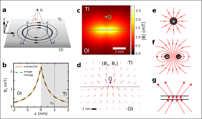
We start by considering the case where a semi-infinite bulk of OI (semiconductor) is placed on top of a semi-infinite bulk of TI, separated by a planar interface. The point charge is located in the TI, at a distance from the interface, see Figure 1(a). We take nm, which is a plausible distance for controlled doping in nanostructured semiconductors.Koenraad and Flatté (2011); Capitani et al. (2019)
Figure 1(b) shows the projection of the magnetic field induced along the axis, which is perpendicular to the planar interface and crosses the charge position. For this simple geometry, the field can be calculated analytically using the image charge method.Qi and Zhang (2011); Yīng and Zülicke (2022); Movilla et al. (2023) The comparison between numerical (solid line) and analytical (dashed line) calculations shows an excellent agreement, which illustrates the quantitative accuracy of the numerical method. The figure also reveals that has a maximum of few mT on the interface. Even if weak, the magnitude of is orders-of-magnitude greater than in millimetric structures, where values of fT are expected,Fechner et al. (2014) and experimental detection of electronic effects under fields of similar magnitude have been reported in quantum nanostructures.Fuhrer et al. (2001) Yet, decays rapidly with the distance from the interface. Along the axis, , with corresponding to the interface plane. Remarkably, this is a magnetic monopole-like decay.Qi and Zhang (2011) The fast decay of the field can also be observed in Figure 1(c), which shows the absolute value on the plane containing . The magnetic field is largely a local effect, arising in the vicinity of the interface under . It follows from the fast decay of that the use of multiple charge dopants may extend the field domain, but not its peak intensity, unless the concentration is very high ( nm-3).
Figure 1(d) is a logarithmic plot showing the magnetic field orientation for the same plane as Fig. 1(c). It is clear from the figure that the orientation of reflects neither a magnetic monopole (Fig. 1(e)), nor the quasi-dipole associated to a circular current (Fig. 1(f)). It has been recently pointed out that, for sufficiently small , the distribution in this setup corresponds to a Pearl vortex instead (Fig. 1(g)).Nogueira and van den Brink (2022)
The deviation of the field orientation from that of a magnetic dipole can be understood by analyzing the Hall current, . As mentioned before, an electrical charge induces a current . Because , with the interface coordinate and a surface vector pointing towards the TI, the sign and intensity of are mainly given by the cross product . As can be seen in Figure 1(a), a point charge generates circular currents . Each of the (infinite) loops behaves as a quasi-dipole, but their superposition does not. It is worth noting that the intensity of the currents is set by two factors:
(i) the distance from ; since scales as , currents will become weaker at longer distances.
(ii) the angle between and ; the cross product becomes null when the two vectors are aligned (right below ), and increase as they become orthogonal (longer distances).
The trade-off between the previous effects leads to the most intense Hall currents taking place for radii , where and form an angle of . Weaker currents are expected closer or farther from , as sketched by the different thickness of the lines in Figure 1(a). The dominating character of such loops impose a magnetic field distribution loosely resembling that of a dipole, albeit with clear deviations originating from the interferences with other loops. The absence of vortices around the inbound and outbound current in Fig. 1(d), as compared to the quasi-dipole of Fig. 1(f), is one example. Another example is that, in Fig. 1(c), the strongest field does not arise around the dominating current (), but for (notice the maxima in the figure take place for lateral displacements smaller than nm from the center). The latter fact is related to the inverse proportionality between and the loop radius , which makes the inner loops have a significant contribution even if they host moderate current .
III.2 Quantum well
A semiconductor quantum well (QW) embedded in a TI material involves two parallel planar interfaces.Harrison and Valavanis (2016) As such, one can design the properties of the induced magnetic field from the superimposed effects of two simple planes, each with a different sign of .
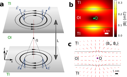
Consider first the high-symmetry case where the charge is in the center of the QW, Figure 2(a). The Hall currents on top and bottom interfaces have the same magnitude but opposite sense of rotation, set by the product . The result is that magnetic fields of identical magnitude but opposite sign are induced on each surface, and these can be expected to cancel out at the position of . This is indeed observed in actual calculations: is suppressed around –Figure 2(b)–, and the field distribution exhibits a nodal plane for at the center of the QW –Figure 2(c)–, which is reminiscent of that arising from two quasi-dipoles of opposite sign. All of these are manifestations of the magnetoelectric interaction between the two QW planes, and set a first example on how nanostructures can be composed to design the resulting magnetic field.
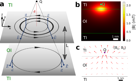
We next consider the case where an off-centered charge is placed in the TI material, at a distance nm from the top of the QW. Figure 3 analyzes the resulting magnetic field. The field is very similar to that of a single plane studied in Fig. 1, because the electric field reaching the bottom interface is already weak, which reduces its influence. A few signatures of the inter-plane interaction can however be observed. Notice in Fig. 3(c) that the field is severely quenched under the QW. This is a consequences of the Hall currents on the bottom plane compensating for those on the top one.Yīng and Zülicke (2022); Movilla et al. (2023)
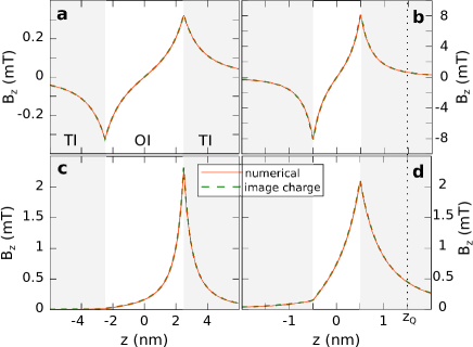
The results in Fig. 2 and 3 correspond to a QW with thickness nm, which is a representative value for epitaxial wellsDurnev (2014). Qualitatively similar results are obtained for narrower QWs, such as colloidal nanoplatelets, which can be as thin as nm.Dabard et al. (2021) To illustrate this point, in Figure 4 we compare the magnetic field along the -axis for QWs of different . Fig. 4(a) and (b) compare induced by a centered charge in QWs with nm and nm, respectively. In both cases, the field is antisymmetric with respect to the plane. The fields are stronger in the narrow QW for the simple reason that is closer to the interface. In the case of off-centered charges, Fig. 4(c) and 4(d), since nm for both QW thicknesses, the maximum value of –around 2 mT–, is fairly unsensitive to .
The accuracy of the numerical results in this section is again supported by the excellent agreement with analytical calculations using series of image chargesYīng and Zülicke (2022); Movilla et al. (2023). We compare the results of the two methods in Fig. 4, using solid and dashed lines, respectively. This provides further support to the reliability of the numerical integration for the more elaborate nanostructures we address in the next sections.
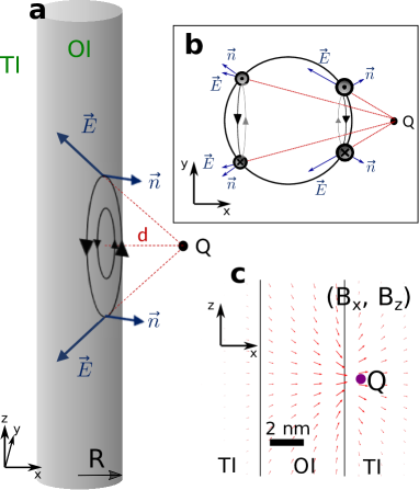
III.3 Quantum wire
We consider now a cylindrical, semiconducting wireHarrison and Valavanis (2016) with radius nm, embedded in a TI material. As we shall see below, the curvature of the quantum wire (QWW) brings about some characteristic features, when compared to the QW.
In a QWW, the high symmetry configuration corresponds to the charge placed at the center of the circular cross section. As shown in Figure 5(a), no Hall currents are expected at any point of the radial boundary of the plane, because and hence . By contrast, radial currents are formed at all distances above and below . Interestingly, the product leads to having opposite sense of rotation in each case. This anticipates another suppression of in the vicinity of , analogous to that of QWs, despite the different geometry. This effect is confirmed by the numerical calculations. In Figure 5(b), shows a clear quenching around . At the same time, in Figure 5(c), the field orientation reveals that the plane containing acts as a nodal plane for .
The magnetic field generated by a centered charge in a QWW closely corresponds to that induced by two quasi-dipoles with opposite sign above and below . In Fig. 5(b), two axially symmetric maxima of the field are observed at . At that position, in Fig. 5(c), vortex-like circulations of the field allow one to identify the positive and negative poles of the dipole, which we represent using standard symbols of inbound () and outbound () current. It is inferred that results mainly from two circular Hall current loops, which prevail over others. The formation of dominating loops can be rationalized through the schematic in Figure 5(a). As mentioned in Section III.1, the intensity of the currents is set by the trade-off between the distance from , which weakens , and the angle between and . As in planar interfaces, this occurs for an angle of , which sets . Unlike in planes and QWs, however, here all the current loops have the same radius , so the most intense currents translate into the strongest .
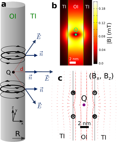
Figure 6 analyzes the magnetic field induced by an off-centered charge , placed outside the QWW. As shown in Fig. 6(a), the Hall currents are no longer circular. Another characteristic feature is that, contrary to the planar interfaces of the QW, here the sign of the Hall currents on the front and back sides of the QWW have the same sign. This can be understood from the diagram in Figure 6(b), which shows a top view of the cross-section containing . No matter the distance from to the wire, the angle between and has the same sign for front and back sides. A direct consequence is that the magnetic field arising on the back interface does not compensate for that of the front one. This implies that the calculated field, plotted in Fig. 6(c), is not suppressed as the back interface is approached, and it can be felt on the opposite side of . This is in sharp contrast with the QW, Figure 3(c). We stress that this behavior results from the circular curvature of the QWW cross-section, but increasing the ellipticity should eventually retrieve the QW behavior. Therefore, one can anticipate the existence of a critical eccentricity at which on the back interface, at which the sign is reversed. A related mechanism has been put forward for semi-spherical cavities, where the sign of the magnetic field can be reversed through the distance between and the center of the sphere.Campos et al. (2017)
III.4 Quantum dot
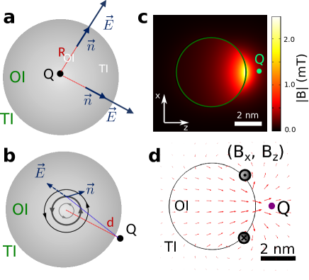
Quantum dots (QDs) exhibit nanometric confinement in all three directions of space.Harrison and Valavanis (2016) When embedded inside a TI, this involves magnetoelectrically polarized boundaries, all within short distances from each other. Sizable interactions may then take build up within them. Combined with the precise synthetic control of their size and shape,Kovalenko et al. (2015) these properties make QD systems particularly suited to modulate the TME. To investigate such interactions, here we consider two basic geometries, namely spherical and cuboidal QDs. QDs with geometries resembling these limit cases are now routinely achieved with colloidal chemistry.Kovalenko et al. (2015)
Figure 7 shows results for a spherical QD. If the source charge is centered, the spherical symmetry of the system leads to all over the boundary, see Fig. 7(a). Therefore, no Hall currents are formed, and no magnetic field is induced. The suppression of the TME is however lifted as soon as the charge is off-centered. Figure 7(b) shows the expected Hall currents triggered by a charge outside the QD. These are spherical and, as in the QWW, have the same sign on the front and back sides of the nanostructure. The ensuing magnetic field intensity is strongest near the QD cap close to the charge, Fig. 7(c), and the field distribution, plotted in Fig. 7(d), exhibits circulating vortices, which makes it reminiscent of a simple quasi-dipole field. This behavior is in contrast to that of a planar interface, Fig. 1(d), and reflects the fact that interferences between concentric Hall currents on the sphere surface are less destructive than those on a plane.
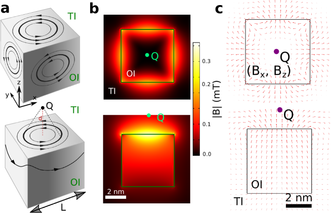
Cuboidal QDs are a paradigmatic example on how the proximity of boundaries in QDs can be manipulated to shape the TME. Compare the Hall currents induced by a charge in the center of a cube or outside it, top and bottom rows of Figure 8(a), respectively. In the former case (top schematic), circular currents with opposite sign form on each pair of parallel faces. These tend to compensate each other, similar to the QW case –Fig. 2(a)–. On the contrary, if the charge is outside (bottom schematic), the Hall currents are similar to those of a simple plane, but with extra currents with same sense of rotation formed on the lateral sides, which reinforce the resulting magnetic field. The constrasting behavior is reflected in Figure 8(b), where is plotted for a cross-section of the QD containing the charge . The cube side is nm and, for the sake of comparison, is placed at nm from the surface both in the centered and off-centered configurations. When is centered (top panel), a broad area with quenched magnetic field is formed. On the contrary, when is off-centered (bottom panel), the resulting field becomes stronger, and a slow decay is observed inside the QD, which is in contrast with the fast decay outside the QD. Both the quenching and the enhancement of the magnetic field are more efficient than those observed in QWs of similar dimensions (cf. Fig. 2(b) and 3(b)). Drastic changes are seen in the field distribution as well depending on the charge location, owing to the cuboidal geometry, see Figure 8(c), with a prominent role played by the cube edges.
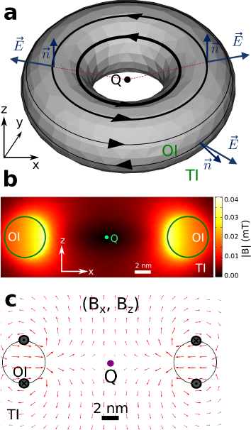
III.5 Quantum ring
Doubly connected, ring-like semiconductor nanostructures have attracted attention in the solid state community for their ability to reveal topological phenomena, such as the Aharonov-Bohm effect in the presence of external magnetic fields.Fuhrer et al. (2001); Fomin (2014) We consider here an ideal, torus-shaped quantum ring (QR). Because the QR can be seen as a bended wire, the magnetic fields induced by off-centered charges close to one side of the QR are similar to those of QWW, albeit with deviations arising from the curvature of the ring arm (not shown). If the charge is centered, however, the analogy is less straightforward.
Analyzing the Hall currents induced by a centered charge, Figure 9(a), one infers that these spin in circles around , with opposite sense of rotation above and below the (equatorial plane), which is again reminiscent of the cylindrical QWW. This behavior is confirmed by the calculated field distribution, plotted in Figure 9(c), which corresponds roughly to that set by two dominant quasi-dipoles, marked by and symbols in the figure. The field intensity, however, is strongest on the inner side of the QR, Figure 9(b). In this regard, the behavior is closer to that of an off-centered charge near a spherical QD, Fig. 7(b).
IV Conclusions
We have introduced a simple numerical model to calculate magnetoelectric fields generated by electrostatic charges in TI-OI heterostructures of arbitrary geometry. The model is quantitatively as accurate as the image charge method, but with the advantadge of providing easy access to non-planar and elaborate geometries. It thus constitutes a fast and versatile tool to build models pursuing specific effects. We have then used the model to invesigate the TME in the most common semiconductor nanostructures: quantum dots, rings, wells and wires. By changing the position of a source electric charge with respect to the nanostructure, the strength and orientation of the resulting magnetic field undergoes severe changes. These results confirm that low-dimensional nanostructures, embedded in TI media, constitute a particularly rich playground to investigate and exploit the TME.
The most conspicuous influence of the nanostructure geometry is observed in cuboidal QDs, where the interactions between boundaries can be used to efficiently enhance or quench the induced magnetic fields.
.
Acknowledgements.
We acknowledge support from MICINN project PID2021-128659NB-I00, UJI project B-2021-06 and Generalitat Valenciana Prometeo project 22I235-CIPROM/2021/078.References
- Wilczek (1987) F. Wilczek, Physical Review Letters 58, 1799 (1987).
- Nenno et al. (2020) D. M. Nenno, C. A. Garcia, J. Gooth, C. Felser, and P. Narang, Nature Reviews Physics 2, 682 (2020).
- Yīng and Zülicke (2022) Y. Yīng and U. Zülicke, Advances in Physics: X 7, 2032343 (2022).
- Bernevig et al. (2006) B. A. Bernevig, T. L. Hughes, and S.-C. Zhang, science 314, 1757 (2006).
- Qi and Zhang (2011) X.-L. Qi and S.-C. Zhang, Reviews of Modern Physics 83, 1057 (2011).
- Maciejko et al. (2010) J. Maciejko, X.-L. Qi, H. D. Drew, and S.-C. Zhang, Physical review letters 105, 166803 (2010).
- Vazifeh and Franz (2010) M. Vazifeh and M. Franz, Physical Review B 82, 233103 (2010).
- Okada et al. (2016) K. N. Okada, Y. Takahashi, M. Mogi, R. Yoshimi, A. Tsukazaki, K. S. Takahashi, N. Ogawa, M. Kawasaki, and Y. Tokura, Nature communications 7, 1 (2016).
- Liu et al. (2020) C. Liu, Y. Wang, H. Li, Y. Wu, Y. Li, J. Li, K. He, Y. Xu, J. Zhang, and Y. Wang, Nature materials 19, 522 (2020).
- Gao et al. (2021) A. Gao, Y.-F. Liu, C. Hu, J.-X. Qiu, C. Tzschaschel, B. Ghosh, S.-C. Ho, D. Bérubé, R. Chen, H. Sun, et al., Nature 595, 521 (2021).
- Yue et al. (2018) C. Yue, S. Jiang, H. Zhu, L. Chen, Q. Sun, and D. W. Zhang, Electronics 7, 225 (2018).
- Jackson (1999) J. D. Jackson, “Classical electrodynamics,” (1999).
- Takagahara (1993) T. Takagahara, Physical Review B 47, 4569 (1993).
- Movilla et al. (2023) J. Movilla, J. Climente, and J. Planelles, in preparation ., . (2023).
- Fechner et al. (2014) M. Fechner, N. A. Spaldin, and I. Dzyaloshinskii, Physical Review B 89, 184415 (2014).
- Campos et al. (2017) W. H. Campos, W. A. Moura-Melo, and J. M. Fonseca, Physics Letters A 381, 417 (2017).
- Martín-Ruiz et al. (2016) A. Martín-Ruiz, M. Cambiaso, and L. Urrutia, Physical Review D 93, 045022 (2016).
- Fuhrer et al. (2001) A. Fuhrer, S. Lüscher, T. Ihn, T. Heinzel, K. Ensslin, W. Wegscheider, and M. Bichler, Nature 413, 822 (2001).
- Bayer et al. (2000) M. Bayer, O. Stern, A. Kuther, and A. Forchel, Physical Review B 61, 7273 (2000).
- Shornikova et al. (2018) E. V. Shornikova, L. Biadala, D. R. Yakovlev, V. F. Sapega, Y. G. Kusrayev, A. A. Mitioglu, M. V. Ballottin, P. C. Christianen, V. V. Belykh, M. V. Kochiev, et al., Nanoscale 10, 646 (2018).
- Malkova and Bryant (2010) N. Malkova and G. W. Bryant, Physical Review B 82, 155314 (2010).
- Kalesaki et al. (2014) E. Kalesaki, C. Delerue, C. M. Smith, W. Beugeling, G. Allan, and D. Vanmaekelbergh, Physical Review X 4, 011010 (2014).
- Beugeling et al. (2015) W. Beugeling, E. Kalesaki, C. Delerue, Y.-M. Niquet, D. Vanmaekelbergh, and C. M. Smith, Nature communications 6, 1 (2015).
- Wan et al. (2017) W. Wan, Y. Yao, L. Sun, C.-C. Liu, and F. Zhang, Advanced Materials 29, 1604788 (2017).
- Ouellet and Bogorad (2019) J. Ouellet and Z. Bogorad, Physical Review D 99, 055010 (2019).
- Martín-Ruiz et al. (2019) A. Martín-Ruiz, M. Cambiaso, and L. Urrutia, International Journal of Modern Physics A 34, 1941002 (2019).
- Dabard et al. (2021) C. Dabard, J. Planelles, H. Po, E. Izquierdo, L. Makke, C. Gréboval, N. Moghaddam, A. Khalili, T. H. Dang, A. Chu, et al., Chemistry of Materials 33, 9252 (2021).
- Geiregat et al. (2018) P. Geiregat, A. J. Houtepen, L. K. Sagar, I. Infante, F. Zapata, V. Grigel, G. Allan, C. Delerue, D. Van Thourhout, and Z. Hens, Nature Materials 17, 35 (2018).
- Pournaghavi et al. (2021) N. Pournaghavi, A. Pertsova, A. MacDonald, and C. M. Canali, Physical Review B 104, L201102 (2021).
- Koenraad and Flatté (2011) P. M. Koenraad and M. E. Flatté, Nature materials 10, 91 (2011).
- Capitani et al. (2019) C. Capitani, V. Pinchetti, G. Gariano, B. Santiago-González, C. Santambrogio, M. Campione, M. Prato, R. Brescia, A. Camellini, F. Bellato, et al., Nano Letters 19, 1307 (2019).
- Nogueira and van den Brink (2022) F. S. Nogueira and J. van den Brink, Physical Review Research 4, 013074 (2022).
- Harrison and Valavanis (2016) P. Harrison and A. Valavanis, Quantum wells, wires and dots: theoretical and computational physics of semiconductor nanostructures (John Wiley & Sons, 2016).
- Durnev (2014) M. Durnev, Physics of the Solid State 56, 1416 (2014).
- Kovalenko et al. (2015) M. V. Kovalenko, L. Manna, A. Cabot, Z. Hens, D. V. Talapin, C. R. Kagan, V. I. Klimov, A. L. Rogach, P. Reiss, D. J. Milliron, et al., ACS nano 9, 1012 (2015).
- Fomin (2014) V. M. e. Fomin, Physics of Quantum Rings (Springer-Verlag, 2014).