Natural band alignment of alloys
Abstract
We have calculated formation enthalpies, band gaps, and natural band alignment for alloys by first principles calculation based on density functional theory. The calculated formation enthalpies show that the alloys exhibit a large miscibilitygap, and a metastable region was found to occur when the S content was below 18% or over 87%. Effect of S incorporation for band gaps of alloys shows large bowing parameter (b 13 eV) induced. The dependence of the band lineup of alloys on the S content by using two different methods, and the change in the energy position of valence band maximum (VBM) was larger than that of conduction band minimum. Based on the calculated VBM positions, we predicted that with S content 10 to 18% can be surface charge transfer doping by high electron affinity materials. The present work provides an example to design for p-type oxysulfide materials.
I INTRODUCTION
Magnesium oxide (MgO) is a non-toxic oxide material commonly used in refractory and medical applications. It has a wide bandgap (7.8 eV) and direct transition type electronic band structure, which is a promising material for optical device applicationOnuma et al. (2021). Despite these attractive physical properties, MgO has only been utilized as a barrier material in electronics applications such as spin-tunneling devicesParkin et al. (2004). This is probably because MgO is considered to be carrier uncontrollable and cannot be used as a semiconductor. However, MgO exhibits a standard semiconducting mechanism where Li doping increases electrical conductivityTardío et al. (2002). Furthermore, in recent years, bandgap engineering has been demonstrated by epitaxial growth of rock-salt (RS) structured MgZnO alloysKaneko et al. (2016a, 2018); Onuma et al. (2018); Ishii et al. (2019); Ono et al. (2019); Gorczyca et al. (2020). Therefore, MgO and MgZnO alloys are attracting attention as new ultra-wide bandgap (UWBG) semiconductorsTsao et al. (2018); Higashiwaki et al. (2021).
Among the known UWBG semiconductors, oxide materials such as \ceGa2O3 and \ceAl2O3 in particular are known to have difficulty with p-type (or ambipolar) dopingYan and Wei (2008). According to the modern theory of doping, some UWBG materials (also MgO) are unable to control their Fermi energy to near the valence band maximum (VBM) or conduction band minimum (CBM)Cao et al. (2019); Goyal et al. (2020); Zunger and Malyi (2021). This dopability trend has been empirically explained by the location of the band edges (i.e., VBM and CBM) relative to the vacuum level (). The empirical criterion indicates that holes can be doped when the VBM is greater than approximately eV, meaning that a shallower VBM is advantageous for p-type doping in oxide materialsRobertson and Clark (2011); Hosono (2013); Robertson and Zhang (2021). P-type wide bandgap oxides such as \ceNiOSawatzky and Allen (1984), \ceCuAlO2Yanagi et al. (2000), \ceSrCu2O2Ohta et al. (2002), and -\ceIr2O3Kan et al. (2018) have been reported hybridized orbitals between O 2p and transition metal d produce shallower VBM than other oxides. Transition metal oxides were found to be suitable for p-type doping, but it is difficult to obtain a UWBG (> 4 eV) using these compounds due to the influence of d electrons with low binding energy. Despite this trade-off, the alloying of -\ceGa2O3 and -\ceIr2O3 has successfully realized p-type UWBG oxidesKaneko et al. (2021); Kaneko and Fujita (2022). In the case of VBM for -(Ir,Ga)2\ceO3, the energy positions depend on the Ga (Ir) atom compositionsKaneko et al. (2021). Thus, attempts to search for p-type UWBG oxides has focused on those containing cation atoms with d-bands.
Another approach to p-type doping involves alloying the semiconductor to raise the host VBM toward and decrease the acceptor level relative to itCao et al. (2019). For example, it was found that when zinc oxide (ZnO) is alloyed with the effect of sulfur (S), the nitrogen () acceptor ionization energy is reduced for pure ZnOPersson et al. (2006). These results indicated that a large VBM shift occurs when the oxygen that predominantly forms the VBM of ZnO is replaced with another anion atom (S). Therefore, the VBM of oxide semiconductors can be better modulated by substituting anion atoms rather than cation atoms. Unfortunately, only a small number of experimental investigations have been conducted on doped p-type because of the strong unintentional n-type doping of ZnOKang et al. (2014); Kobayashi et al. (2017). Thus the well-established studies of cation-substituted II-VI semiconductor alloys, there are few reports on anion-substituted onesAdachi (2009). Therefore, the common-cation systems such as alloys should be investigated not only for p-type doping of UWBG materials, but also for future oxysulfide (or oxychalcogenides) applicationsWoods-Robinson et al. (2020).
In this paper, we address to analyze the effect of sulfur incorporation on MgO by using first principles calculation based on density functional theory (DFT). The formation enthalpies and band gap of alloys were investigated, and the natural band alignment of the alloys was also derived from the calculations to predict doping tendency. Moreover, we proposed to combine alloys with high electron affinity materials that could induce hole carriers by surface charge transfer doping (SCTD).
II CALCULATION DETAILS
We modeled the supercell structure of the alloy; the alloy cells contained 16 atoms, namely 8 Mg and 8 O (S) atoms. To consider only inequivalent cells due to the atomic substitution, we employed a supercell programOkhotnikov et al. (2016). The geometry optimization was performed using the Quantum ESPRESSO packageGiannozzi et al. (2009, 2017). We used the Perdew-Burke-Ernzerhof form within the generalized gradient approximation with projector-augmented wave potentialsPerdew et al. (1996); Blöchl (1994). The electronic wavefunctions and charge densities were expanded in plane waves with cut-off energies of 65 and 450 Ry, respectively. The k-points were generated using the Monkhorst-Pack scheme with a mesh size of 8 8 8 for optimizing the structure calculationsMonkhorst and Pack (1976). To optimize the model geometry, the stress and force on the atoms were set to 0.05 GPa and 0.1 mRy/a.u., respectively. After optimizing the model geometry, the most favorable alloy structures were determined using the formation enthalpy. The formation enthalpy, , was calculated according to
| (1) |
where E and E are the energies of the lowest RS structures. A regular solution model for alloy energies can be described as
| (2) |
and represented critical formation enthalpyNeugebauer and Van de Walle (1995). The growth temperature prediction using following equation
| (3) |
where is the Boltzmann constantNeugebauer and Van de Walle (1995). All favorable alloy structures were considered to calculate the electronic band structures using the Wien2k codeBlaha et al. (2020). The calculation details are provided as supplementary information. To determine the natural band edge positions of the alloys using the two-alignment method, we employed a modified Tersoff methodSchleife et al. (2009) for the branch point energy () and the atomic solid-state energy (SSE) scale approachOta (2020). Originally, means mid gap energy of semiconductor, which is given by averaged valence and conduction band energies. The is here approximated as
| (4) |
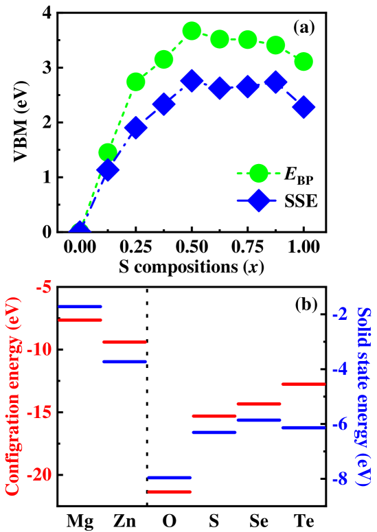
where is the number of points in the meshes in the Brillouin zone, and and are the ith lowest conduction band and jth highest valence band states at the wave vector k, respectively. We calculated using 8 and 16 for the alloy structures, and 2 and 1 for the primitive structures, such as MgO and MgS. An atomic SSE was determined by an averaged electron affinity (for a cation atom) or an ionization potential (for an anion atom) for several inorganic compoundsPelatt et al. (2011). The SSE scale approach can be determined natural band alignment using the SSE and band gap of materialOta (2020). 1.72, 7.98, and 6.31 eV were used as the absolute values of the atomic SSEs of Mg, O, and S, respectivelyPelatt et al. (2015).
III Results and Discussions
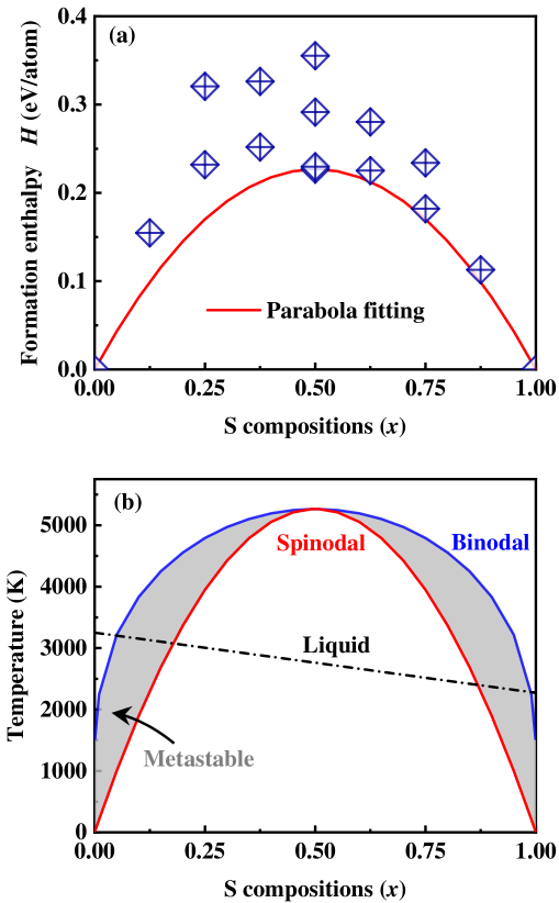
Figure 1 (a) shows the formation enthalpy per atom of alloys based on the use of all nonequivalent atomic substitution models. In this calculation, we did not consider the wurtzite structure or the alloy mixing enthalpy. We have estimated critical formation enthalpy ( = 227 meV) by equation 2 parabola fitting. The growth temperatures of alloys using and equation 3 are depicted in Fig.1 (b). These results show alloys single crystal growth is difficult in thermal equilibrium conditionsMillican et al. (2020). However, metastable regions exist in S concentrations less than 18% and S more than 87% below the liquidus line. Therefore, we believe that the crystal growth of alloys can be achieved by the mist chemical vapor deposition (CVD) method, which is suitable for the growth of oxide metastable structures and their alloysShinohara and Fujita (2008); Ito et al. (2012); Fujita and Kaneko (2014); Suzuki et al. (2014); Kaneko et al. (2016b); Fujita et al. (2016); Oshima et al. (2017); Dang et al. (2018); Jinno et al. (2018); Tahara et al. (2018); Nishinaka et al. (2018); Horie et al. (2021); Takane et al. (2021); Ogura et al. (2022); Biswas and Nishinaka (2022); Nishinaka et al. (2022); Kaneko et al. (2022); Takane et al. (2022). Indeed, mist CVD has succeeded in synthesizing sulfides such as \ceZnSUno et al. (2016a, b, 2017); Okita et al. (2018) and \ceCu2SnS3Okamura et al. (2022), and the growth of metastable alloys is a future challenge. Note that the S compositions outside of metastable regions in Fig.1 (b), alloys may grow in an amorphous phaseJaquez et al. (2019).
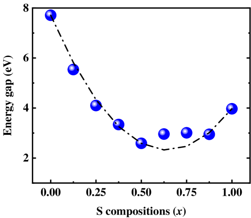
To estimate the bandgap () of alloys, we calculated the lowest models using the Wien2k code. The result is shown in Figure 2. The dependence on the S content of the alloy was determined using the Tran–Blaha modified Becke Johnson potentialTran and Blaha (2009); Koller et al. (2012). The calculated trend of as a function of the S content exhibits the same nonlinear relationship behavior as that experimentally observed for wurtzite structured alloysMeyer et al. (2004). The of alloys is described as
| (5) |
where is the bowing parameter, and the bandgap energies [MgO] and [MgS] are 7.71 and 3.91 eV, respectively. We estimated that the bowing parameter is approximately 13 eV due to the large difference in the values between MgO and MgS. This large bowing parameter is similar to that of corundum structured (b 19 eV)Liu et al. (2021), wurtzite structured (b 16.9 eV)Kimura et al. (2004), (b 28.3 eV)Borovac et al. (2018), and (b 30.5 eV)Tan et al. (2016) structures, and it is thought that large bowing parameters are a unique feature of highly mismatched alloys with a large difference in . Note that the of MgO agrees well with the experimental value. By contrast, the of MgS is difficult to compare with the calculation results because there are few experimental reports for this material. However, our calculated value of 3.91 eV seems reasonable for the RS-structured MgS since previous theoretical calculations have reported values ranging between 3.2 and 4.8 eVBhandari et al. (2018), and experimental studies have measured values ranging between 3.5 and 4.1 eVTaleatu et al. (2015). Therefore, our calculated values of the alloys are suitable for band alignment estimation.
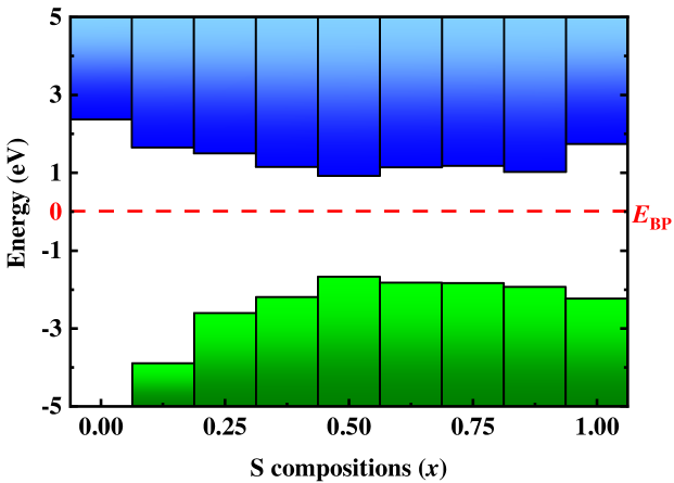
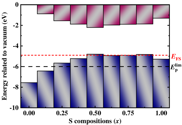
The resulting natural band lineups to are plotted in Figure 3; they are aligned with respect to the red dotted line. The represents a charge neutrality level (CNL), which marks the energy where defect states change their character from predominantly donor-like (acceptor-like). Unintentional heavy p-type doping is expected to occur when the line overlaps or below the VBMSarmadian et al. (2016). This shows that the energy formation of acceptor-type defects becomes smaller than that of donor-type defectsKing et al. (2009). According to this simple classification concept, we can infer that the closer the is to the VBM of the alloys, the higher the potential will be for p-type doping. The lowest (1.67 eV) occurred for the case; this value is significantly lower than that of MgO ( = 5.34 eV). However, the tunability of the VBM position with the S content is lost at approximately 2 eV below the . The natural band lineup result indicates that S incorporation enhances the possibility of p-type doping, although the modified Tersoff method does not provide band edge positions on an absolute energy scale. Therefore, we employed the atomic SSE approach to evaluate the band discontinuities of alloys. The natural band alignment relative to the of the alloys is illustrated in Figure 4. The different trends of each band edge position as a function of the S content were found to be consistent with Figure 3. Here we estimated the possibility of achieving p-type doping of alloys using several doping limitation indicators. Some works have presented universal CNLsOta et al. (2022), such as the hydrogen levelVan de Walle and Neugebauer (2003), limiting Fermi level ()Brudnyĭ et al. (2007), and Fermi level stabilization energy ()Walukiewicz (2001). The level, , and are located at about , Brudnyi et al. (2004), and eV below , respectively. These CNLs are indicators used to discriminate whether extrinsic defects or hydrogen are donors or acceptors depending on the Fermi level in a material. However, in this work, we focus only on the deepest level from . Moreover, following the empirical rule, hole doping of oxide is possible when the VBM is located above approximately eVRobertson and Clark (2011); Hosono (2013); Robertson and Zhang (2021). These different indicators originate from different approaches; they all seem to indicate the intrinsic doping criteria for semiconductors. According to the empirical rule (), our calculated band lineup of the alloys shows that hole doping becomes possible when exceeds 0.25. Such a trend is understandable given the using the amphoteric native defect modelWalukiewicz (2001). As shown in Figure 4, the VBM of (0.5 x 0.875) is located almost at the , which explains the strong possibility for p-type doping at these S compositions. Since the smaller the energy difference , the larger the maximum hole carrier concentration, alloys are expected to exhibit enhanced p-type conduction with respect to MgOTokumitsu (1990). Therefore, the empirical rule and the trends are consistent as p-type dopability indicators. We note that the finding suitable dopants for an alloy is difficult with the current DFT calculation framework.
Although Figure 4 shows a trend similar to the VBM change obtained via the result, it reveals a larger hole-doping possibility than Figure 3. Note that in several recent studies, the modified Tersoff method () has not correctly predicted the p-type dopability trendYim et al. (2018); Woods-Robinson et al. (2018); Brunin et al. (2019). Consequently, we expect the value and the empirical rule () to be better predictors of p-type doping criteria. These band alignment results indicate that doping MgO with both electrons and holes is extremely difficult. For example, lithium (Li) is a deep acceptor level in MgO, and its activation energy has been reported to be about 0.7 eVTardío et al. (2002). However, the Li acceptor activation energy is expected to decrease as the VBM moves upward upon S alloyingGoodrich et al. (2021). Furthermore, since the defect and impurity levels are determined by the host materialHuang et al. (2015), S concentrations of about 25% or less for alloys can be expected to lower the Li acceptor levels by increasing the energy position of the VBM, as in the case of alloysPersson et al. (2006). Additionally, universal levels of oxygenChakrapani (2021) and transition metal impuritiesCaldas et al. (1984); Zunger (1985) have been reported, and these could become shallow acceptor levels through VBM modulation. This experimental evidence is not yet available; however, a theoretical result based on defect formation energy calculations suggested that MgS is a p-type transparent conducting material candidateRaghupathy et al. (2018); Li and Singh (2019). This result is consistent with those based on the empirical rule and the predictions, and we thus believe that our calculations can correctly predict the p-type dopability criteria.
The calculated relative VBM positions (VBM) concerning MgO are shown in Figure 5 (a). These results indicate that the increasing trends of the natural valence band offset of with increasing S content obtained using different approaches are consistent. The offset value trend can be explained as a chemical trend by considering the atomic energy of common anions, such as O, S, Se, and Te atoms. Figure 5 (b) shows the atomic energy levels, including the configuration energy (CE)Mann et al. (2000) and SSEPelatt et al. (2015) for each atom. The energies of these VI-group atoms become closer to as the atomic number increases, except for the SSE of Te atoms. CE refers to the energy of isolated atoms, whereas SSE refers to the energy of “atoms in a crystal”, such as the Bader charge conceptBader (1985). Our calculation results can be explained by the SSE more simply than those derived from the CE. For example, a rough estimate of can be obtained by calculating the difference in SSE between cation atoms, such as Mg and Zn, and anion atoms (cf. Figure 5 (b))Pelatt et al. (2011). The VBM of can be determined by calculating the difference in the SSE scale between S and O atoms. These findings indicate that the energy levels of atoms in a crystal are determined by the oxidation (or reduction) statePelatt et al. (2019). Therefore, the energy position of the VBM of ionic bonded materials can be modulated via anion atom substitutions. We note that the VBM modulation is only possible when anion atoms dominate the top of the valence band of the material (see Supporting information Figures S1-S9). These results clearly show that Mg atoms contribute little to the valence band in the energy range of 0 eV.
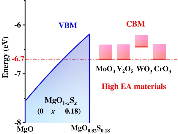
From our band alignment results, we have considered hole doping by SCTDChen et al. (2009). The SCTD technique has been demonstrated for hydrogenated diamondsCrawford et al. (2021) and several inorganic semiconductors : grapheneChen et al. (2007), siliconRietwyk et al. (2014), cubic boron nitrideHe et al. (2015), and perovskite materialsEuvrard et al. (2021). In order to holes doping spontaneously, we have to contact the high electron affinity (EA) or high work function materials with alloys. Here we have investigated whether SCTD occurs for metastable condition (x 0.18) with over 4 eV shown in Fig 6. The high EA materials are approximately 6.7 eV for \ceMoO3Kröger et al. (2009), \ceV2O5Meyer et al. (2011), \ceCrO3Greiner et al. (2012), and approximately 6.45 eV for \ceWO3Meyer et al. (2010), respectively. The results indicated that the surface charge transfer appeared spontaneously at S content above 10% for alloys in contact with high EA materials except for \ceWO3. Note that the energetic positions of the VBM for alloys are calculated by the SSE scale approach, while the CBMs for high EA materials are experimental values. These high EA materials induced sheet hole carrier concentrations greater than cm-2 with respect to hydrogenated diamondVerona et al. (2016); Crawford et al. (2021). Thus, the sheet hole carrier concentration of alloys is expected to be the same order of magnitude hydrogenated diamond by SCTD. This is consistent with the number of adsorbed molecules on the MgO (100) or (111) surfaceOnishi et al. (1987), and the sheet hole carriers are expected to be tunable around cm-2. Other potential surface charge-induced phenomena include defect modulation dopingWeidner et al. (2019), formal (or surface) polarization effectsZhou et al. (2015); Adamski et al. (2020), and electrochemical doping Ishii et al. (1999); Wang et al. (2017); Rietwyk et al. (2019); Wang et al. (2019). These phenomena are different from bulk doping but show that holes can be generated by using appropriate surface or interface effects. Therefore, these SCTD schemes must be adopted instead of conventional impurity doping to realize p-type UWBG oxide semiconductors.
IV Conclusion
We have investigated the S incorporation effect of MgO using a first principles calculation based on DFT. Our results indicated that the solubility of S content required for the metastable solid phase of the alloys was estimated to be less than 18% or over 87%, respectively. The band gap of alloys became the smallest at 50% S content, and the bowing parameter was estimated b 13 eV. Our calculated natural band alignment indicated that the alloys tend to be more easily doped to p-type than n-type. Based on the calculated VBM positions, we predicted that metastable with S content of 10 to 18% can be SCTD by high EA materials. We hope that the present work may provide design guidelines for p-type oxysulfide materials.
Acknowledgements.
This work was supported in part by Grants-in-Aid for Scientific Research No. 20H00246 from MEXT, Japan.AUTHOR DECLARATIONS
Conflict of Interest
The authors have no conflicts to disclose.
Supplementary Material
Details of the DFT calculations and their results are provided in the supplementary materials.
Author Contributions
Yuichi Ota: Conceptualization (equal); Data curation (lead); Formal analysis (lead); Methodology (lead); Investigation (lead); Writing – original draft (lead); Writing – review & editing (lead). Kentaro Kaneko: Data curation (equal); Formal analysis (equal); Investigation (equal); Writing – review & editing (equal). Takeyoshi Onuma: Data curation (equal); Formal analysis (equal); Investigation (equal); Writing – review & editing (equal). Shizuo Fujita: Conceptualization (lead); Funding acquisition (lead); Project administration (lead); Supervision (lead); Validation (lead); Writing – review & editing (equal).
DATA AVAILABILITY
The data that supports the findings of this study are available within the article and its supplementary material.
References
- Onuma et al. (2021) T. Onuma, W. Kosaka, K. Kudo, Y. Ota, T. Yamaguchi, K. Kaneko, S. Fujita, and T. Honda, Applied Physics Letters 119, 132105 (2021).
- Parkin et al. (2004) S. S. Parkin, C. Kaiser, A. Panchula, P. M. Rice, B. Hughes, M. Samant, and S.-H. Yang, Nature materials 3, 862 (2004).
- Tardío et al. (2002) M. Tardío, R. Ramírez, R. González, and Y. Chen, Physical Review B 66, 134202 (2002).
- Kaneko et al. (2016a) K. Kaneko, T. Onuma, K. Tsumura, T. Uchida, R. Jinno, T. Yamaguchi, T. Honda, and S. Fujita, Applied Physics Express 9, 111102 (2016a).
- Kaneko et al. (2018) K. Kaneko, K. Tsumura, K. Ishii, T. Onuma, T. Honda, and S. Fujita, Journal of Electronic Materials 47 (2018).
- Onuma et al. (2018) T. Onuma, M. Ono, K. Ishii, K. Kaneko, T. Yamaguchi, S. Fujita, and T. Honda, Applied Physics Letters 113, 061903 (2018).
- Ishii et al. (2019) K. Ishii, M. Ono, K. Kaneko, T. Onuma, T. Honda, and S. Fujita, Applied Physics Express 12, 052011 (2019).
- Ono et al. (2019) M. Ono, K. Ishii, K. Kaneko, T. Yamaguchi, T. Honda, S. Fujita, and T. Onuma, Journal of Applied Physics 125, 225108 (2019).
- Gorczyca et al. (2020) I. Gorczyca, M. Wierzbowska, D. Jarosz, J. Domagala, A. Reszka, D. L. S. Dang, F. Donatini, N. Christensen, and H. Teisseyre, Physical Review B 101, 245202 (2020).
- Tsao et al. (2018) J. Tsao, S. Chowdhury, M. Hollis, D. Jena, N. Johnson, K. Jones, R. Kaplar, S. Rajan, C. Van de Walle, E. Bellotti, et al., Advanced Electronic Materials 4, 1600501 (2018).
- Higashiwaki et al. (2021) M. Higashiwaki, R. Kaplar, J. Pernot, and H. Zhao, “Ultrawide bandgap semiconductors,” (2021).
- Yan and Wei (2008) Y. Yan and S.-H. Wei, physica status solidi (b) 245, 641 (2008).
- Cao et al. (2019) R. Cao, H.-X. Deng, and J.-W. Luo, ACS applied materials & interfaces 11, 24837 (2019).
- Goyal et al. (2020) A. Goyal, P. Gorai, S. Anand, E. S. Toberer, G. J. Snyder, and V. Stevanovic, Chemistry of Materials 32, 4467 (2020).
- Zunger and Malyi (2021) A. Zunger and O. I. Malyi, Chemical Reviews 121, 3031 (2021).
- Robertson and Clark (2011) J. Robertson and S. Clark, Physical Review B 83, 075205 (2011).
- Hosono (2013) H. Hosono, Japanese Journal of Applied Physics 52, 090001 (2013).
- Robertson and Zhang (2021) J. Robertson and Z. Zhang, MRS Bulletin , 1 (2021).
- Sawatzky and Allen (1984) G. Sawatzky and J. Allen, Physical review letters 53, 2339 (1984).
- Yanagi et al. (2000) H. Yanagi, S.-i. Inoue, K. Ueda, H. Kawazoe, H. Hosono, and N. Hamada, Journal of Applied Physics 88, 4159 (2000).
- Ohta et al. (2002) H. Ohta, M. Orita, M. Hirano, I. Yagi, K. Ueda, and H. Hosono, Journal of applied physics 91, 3074 (2002).
- Kan et al. (2018) S.-i. Kan, S. Takemoto, K. Kaneko, I. Takahashi, M. Sugimoto, T. Shinohe, and S. Fujita, Applied Physics Letters 113, 212104 (2018).
- Kaneko et al. (2021) K. Kaneko, Y. Masuda, S.-i. Kan, I. Takahashi, Y. Kato, T. Shinohe, and S. Fujita, Applied Physics Letters 118, 102104 (2021).
- Kaneko and Fujita (2022) K. Kaneko and S. Fujita, Journal of Materials Research 37, 651 (2022).
- Persson et al. (2006) C. Persson, C. Platzer-Björkman, J. Malmström, T. Törndahl, and M. Edoff, Physical review letters 97, 146403 (2006).
- Kang et al. (2014) J.-W. Kang, Y.-S. Choi, B.-H. Kim, N.-Y. Kim, C. Tu, and S.-J. Park, Scripta Materialia 84, 39 (2014).
- Kobayashi et al. (2017) K. Kobayashi, T. Ohtsuki, Y. Tomita, Y. Kohno, Y. Maeda, and S. Matsushima, Journal of Crystal Growth 457, 289 (2017).
- Adachi (2009) S. Adachi, Properties of semiconductor alloys: group-IV, III-V and II-VI semiconductors (John Wiley & Sons, 2009).
- Woods-Robinson et al. (2020) R. Woods-Robinson, Y. Han, H. Zhang, T. Ablekim, I. Khan, K. A. Persson, and A. Zakutayev, Chemical reviews 120, 4007 (2020).
- Okhotnikov et al. (2016) K. Okhotnikov, T. Charpentier, and S. Cadars, Journal of Cheminformatics 8, 17 (2016).
- Giannozzi et al. (2009) P. Giannozzi, S. Baroni, N. Bonini, M. Calandra, R. Car, C. Cavazzoni, D. Ceresoli, G. L. Chiarotti, M. Cococcioni, I. Dabo, et al., Journal of Physics: Condensed Matter 21, 395502 (2009).
- Giannozzi et al. (2017) P. Giannozzi, O. Andreussi, T. Brumme, O. Bunau, M. B. Nardelli, M. Calandra, R. Car, C. Cavazzoni, D. Ceresoli, M. Cococcioni, et al., Journal of Physics: Condensed Matter 29, 465901 (2017).
- Perdew et al. (1996) J. P. Perdew, K. Burke, and M. Ernzerhof, Physical Review Letters 77, 3865 (1996).
- Blöchl (1994) P. E. Blöchl, Physical Review B 50, 17953 (1994).
- Monkhorst and Pack (1976) H. J. Monkhorst and J. D. Pack, Physical Review B 13, 5188 (1976).
- Neugebauer and Van de Walle (1995) J. Neugebauer and C. G. Van de Walle, Physical Review B 51, 10568 (1995).
- Blaha et al. (2020) P. Blaha, K. Schwarz, F. Tran, R. Laskowski, G. K. Madsen, and L. D. Marks, The Journal of Chemical Physics 152, 074101 (2020).
- Schleife et al. (2009) A. Schleife, F. Fuchs, C. Rödl, J. Furthmüller, and F. Bechstedt, Applied Physics Letters 94, 012104 (2009).
- Ota (2020) Y. Ota, AIP Advances 10, 125321 (2020).
- Pelatt et al. (2011) B. D. Pelatt, R. Ravichandran, J. F. Wager, and D. A. Keszler, Journal of the American Chemical Society 133, 16852 (2011).
- Pelatt et al. (2015) B. D. Pelatt, R. S. Kokenyesi, R. Ravichandran, C. B. Pereira, J. F. Wager, and D. A. Keszler, Journal of Solid State Chemistry 231, 138 (2015).
- Millican et al. (2020) S. L. Millican, J. M. Clary, C. J. Bartel, N. R. Singstock, A. M. Holder, and C. B. Musgrave, arXiv preprint arXiv:2011.06628 (2020).
- Shinohara and Fujita (2008) D. Shinohara and S. Fujita, Japanese Journal of Applied Physics 47, 7311 (2008).
- Ito et al. (2012) H. Ito, K. Kaneko, and S. Fujita, Japanese Journal of Applied Physics 51, 100207 (2012).
- Fujita and Kaneko (2014) S. Fujita and K. Kaneko, Journal of crystal growth 401, 588 (2014).
- Suzuki et al. (2014) N. Suzuki, K. Kaneko, and S. Fujita, Journal of crystal growth 401, 670 (2014).
- Kaneko et al. (2016b) K. Kaneko, K. Suzuki, Y. Ito, and S. Fujita, Journal of Crystal Growth 436, 150 (2016b).
- Fujita et al. (2016) S. Fujita, M. Oda, K. Kaneko, and T. Hitora, Japanese Journal of Applied Physics 55, 1202A3 (2016).
- Oshima et al. (2017) T. Oshima, Y. Kato, M. Oda, T. Hitora, and M. Kasu, Applied Physics Express 10, 051104 (2017).
- Dang et al. (2018) G. Dang, T. Yasuoka, Y. Tagashira, T. Tadokoro, W. Theiss, and T. Kawaharamura, Applied Physics Letters 113, 062102 (2018).
- Jinno et al. (2018) R. Jinno, T. Uchida, K. Kaneko, and S. Fujita, physica status solidi (b) 255, 1700326 (2018).
- Tahara et al. (2018) D. Tahara, H. Nishinaka, S. Morimoto, and M. Yoshimoto, Applied Physics Letters 112, 152102 (2018).
- Nishinaka et al. (2018) H. Nishinaka, N. Miyauchi, D. Tahara, S. Morimoto, and M. Yoshimoto, CrystEngComm 20, 1882 (2018).
- Horie et al. (2021) R. Horie, H. Nishinaka, D. Tahara, and M. Yoshimoto, Journal of Alloys and Compounds 851, 156927 (2021).
- Takane et al. (2021) H. Takane, K. Kaneko, Y. Ota, and S. Fujita, Japanese Journal of Applied Physics 60, 055501 (2021).
- Ogura et al. (2022) Y. Ogura, Y. Arata, H. Nishinaka, and M. Yoshimoto, Japanese Journal of Applied Physics 61, SC1037 (2022).
- Biswas and Nishinaka (2022) M. Biswas and H. Nishinaka, APL Materials 10, 060701 (2022).
- Nishinaka et al. (2022) H. Nishinaka, O. Ueda, N. Ikenaga, N. Hasuike, and M. Yoshimoto, Materials Letters: X , 100149 (2022).
- Kaneko et al. (2022) K. Kaneko, K. Uno, R. Jinno, and S. Fujita, Journal of Applied Physics 131, 090902 (2022).
- Takane et al. (2022) H. Takane, Y. Ota, T. Wakamatsu, T. Araki, K. Tanaka, and K. Kaneko, Physical Review Materials 6, 084604 (2022).
- Uno et al. (2016a) K. Uno, Y. Yamasaki, P. Gu, and I. Tanaka, physica status solidi (c) 13, 448 (2016a).
- Uno et al. (2016b) K. Uno, Y. Yamasaki, and I. Tanaka, Applied Physics Express 10, 015502 (2016b).
- Uno et al. (2017) K. Uno, Y. Asano, and I. Tanaka, physica status solidi (b) 254, 1600544 (2017).
- Okita et al. (2018) K. Okita, K. Inaba, Z. Yatabe, and Y. Nakamura, Japanese Journal of Applied Physics 57, 065503 (2018).
- Okamura et al. (2022) K. Okamura, R. Saito, A. Kanai, and K. Tanaka, Applied Physics A 128, 1 (2022).
- Jaquez et al. (2019) M. Jaquez, P. Specht, K. M. Yu, W. Walukiewicz, and O. D. Dubon, Journal of Applied Physics 126, 105708 (2019).
- Tran and Blaha (2009) F. Tran and P. Blaha, Physical review letters 102, 226401 (2009).
- Koller et al. (2012) D. Koller, F. Tran, and P. Blaha, Physical Review B 85, 155109 (2012).
- Meyer et al. (2004) B. Meyer, A. Polity, B. Farangis, Y. He, D. Hasselkamp, T. Krämer, and C. Wang, Applied physics letters 85, 4929 (2004).
- Liu et al. (2021) X. Liu, S. Ober, W. Tang, and C.-K. Tan, Journal of Materials Chemistry C 9, 7436 (2021).
- Kimura et al. (2004) A. Kimura, C. A. Paulson, H. Tang, and T. F. Kuech, Applied physics letters 84, 1489 (2004).
- Borovac et al. (2018) D. Borovac, C.-K. Tan, and N. Tansu, AIP Advances 8, 085119 (2018).
- Tan et al. (2016) C.-K. Tan, D. Borovac, W. Sun, and N. Tansu, Scientific Reports 6, 1 (2016).
- Bhandari et al. (2018) U. Bhandari, C. O. Bamba, Y. Malozovsky, D. Bagayoko, et al., Journal of Modern Physics 9, 1773 (2018), and references therein.
- Taleatu et al. (2015) B. Taleatu, E. Omotoso, E. Arbab, R. Lasisi, W. Makinde, and G. Mola, Applied Physics A 118, 539 (2015).
- Sarmadian et al. (2016) N. Sarmadian, R. Saniz, B. Partoens, and D. Lamoen, Scientific reports 6, 1 (2016).
- King et al. (2009) P. King, T. Veal, P. Jefferson, J. Zúñiga-Pérez, V. Muñoz-Sanjosé, and C. F. McConville, Physical Review B 79, 035203 (2009).
- Ota et al. (2022) Y. Ota, M. Imura, R. G. Banal, and Y. Koide, Journal of Physics D: Applied Physics 55, 455102 (2022).
- Van de Walle and Neugebauer (2003) C. G. Van de Walle and J. Neugebauer, Nature 423, 626 (2003).
- Brudnyĭ et al. (2007) V. Brudnyĭ, N. Kolin, and L. Smirnov, Semiconductors 41, 1011 (2007).
- Walukiewicz (2001) W. Walukiewicz, Physica B: Condensed Matter 302-303, 123 (2001).
- Brudnyi et al. (2004) V. Brudnyi, S. Grinyaev, and N. Kolin, Physica B: Condensed Matter 348, 213 (2004).
- Tokumitsu (1990) E. Tokumitsu, Japanese journal of applied physics 29, L698 (1990).
- Yim et al. (2018) K. Yim, Y. Youn, M. Lee, D. Yoo, J. Lee, S. H. Cho, and S. Han, npj Computational Materials 4, 17 (2018).
- Woods-Robinson et al. (2018) R. Woods-Robinson, D. Broberg, A. Faghaninia, A. Jain, S. S. Dwaraknath, and K. A. Persson, Chemistry of Materials 30, 8375 (2018).
- Brunin et al. (2019) G. Brunin, F. Ricci, V.-A. Ha, G.-M. Rignanese, and G. Hautier, npj Computational Materials 5, 1 (2019).
- Goodrich et al. (2021) J. C. Goodrich, C.-K. Tan, D. Borovac, and N. Tansu, Applied Physics Letters 118, 072106 (2021).
- Huang et al. (2015) B. Huang, M. Yoon, B. G. Sumpter, S.-H. Wei, and F. Liu, Physical review letters 115, 126806 (2015).
- Chakrapani (2021) V. Chakrapani, Applied Physics Letters 119, 021601 (2021).
- Caldas et al. (1984) M. J. Caldas, A. Fazzio, and A. Zunger, Applied Physics Letters 45, 671 (1984).
- Zunger (1985) A. Zunger, Annual Review of Materials Science 15, 411 (1985).
- Raghupathy et al. (2018) R. K. M. Raghupathy, T. D. Kühne, C. Felser, and H. Mirhosseini, Journal of Materials Chemistry C 6, 541 (2018).
- Li and Singh (2019) Y. Li and D. J. Singh, Journal of Materials Chemistry C 7, 2436 (2019).
- Mann et al. (2000) J. B. Mann, T. L. Meek, and L. C. Allen, Journal of the American Chemical Society 122, 2780 (2000).
- Bader (1985) R. F. Bader, Accounts of Chemical Research 18, 9 (1985).
- Pelatt et al. (2019) B. D. Pelatt, J. F. Wager, and D. A. Keszler, Journal of Solid State Chemistry 274, 337 (2019).
- Chen et al. (2009) W. Chen, D. Qi, X. Gao, and A. T. S. Wee, Progress in Surface Science 84, 279 (2009).
- Crawford et al. (2021) K. G. Crawford, I. Maini, D. A. Macdonald, and D. A. Moran, Progress in Surface Science 96, 100613 (2021).
- Chen et al. (2007) W. Chen, S. Chen, D. C. Qi, X. Y. Gao, and A. T. S. Wee, Journal of the American Chemical Society 129, 10418 (2007).
- Rietwyk et al. (2014) K. J. Rietwyk, Y. Smets, M. Bashouti, S. H. Christiansen, A. Schenk, A. Tadich, M. T. Edmonds, J. Ristein, L. Ley, and C. I. Pakes, Physical Review Letters 112, 155502 (2014).
- He et al. (2015) B. He, T.-W. Ng, M.-F. Lo, C.-S. Lee, and W. Zhang, ACS Applied Materials & Interfaces 7, 9851 (2015).
- Euvrard et al. (2021) J. Euvrard, Y. Yan, and D. B. Mitzi, Nature Reviews Materials 6, 531 (2021).
- Kröger et al. (2009) M. Kröger, S. Hamwi, J. Meyer, T. Riedl, W. Kowalsky, and A. Kahn, Applied physics letters 95, 251 (2009).
- Meyer et al. (2011) J. Meyer, K. Zilberberg, T. Riedl, and A. Kahn, Journal of Applied Physics 110, 033710 (2011).
- Greiner et al. (2012) M. T. Greiner, M. G. Helander, W.-M. Tang, Z.-B. Wang, J. Qiu, and Z.-H. Lu, Nature materials 11, 76 (2012).
- Meyer et al. (2010) J. Meyer, M. Kröger, S. Hamwi, F. Gnam, T. Riedl, W. Kowalsky, and A. Kahn, Applied Physics Letters 96, 93 (2010).
- Verona et al. (2016) C. Verona, W. Ciccognani, S. Colangeli, E. Limiti, M. Marinelli, and G. Verona-Rinati, Journal of Applied Physics 120, 025104 (2016).
- Onishi et al. (1987) H. Onishi, C. Egawa, T. Aruga, and Y. Iwasawa, Surface Science 191, 479 (1987).
- Weidner et al. (2019) M. Weidner, A. Fuchs, T. J. Bayer, K. Rachut, P. Schnell, G. K. Deyu, and A. Klein, Advanced Functional Materials 29, 1807906 (2019).
- Zhou et al. (2015) Y. Zhou, K. M. Rabe, and D. Vanderbilt, Physical Review B 92, 041102 (2015).
- Adamski et al. (2020) N. L. Adamski, C. E. Dreyer, and C. G. Van de Walle, Physical Review B 102, 201301 (2020).
- Ishii et al. (1999) H. Ishii, K. Sugiyama, E. Ito, and K. Seki, Advanced materials 11, 605 (1999).
- Wang et al. (2017) Q. Wang, A. Puntambekar, and V. Chakrapani, The Journal of Chemical Physics 147, 104703 (2017).
- Rietwyk et al. (2019) K. J. Rietwyk, D. A. Keller, A. Ginsburg, H.-N. Barad, M. Priel, K. Majhi, Z. Yan, S. Tirosh, A. Y. Anderson, L. Ley, et al., Advanced Materials Interfaces 6, 1802058 (2019).
- Wang et al. (2019) Q. Wang, S. Joshi, N. Smieszek, and V. Chakrapani, Journal of Applied Physics 126, 225301 (2019).