Room-temperature exceptional-point-driven polariton lasing from perovskite metasurface
Abstract
Excitons in lead bromide perovskites exhibit high binding energy and high oscillator strength, allowing for a strong light-matter coupling regime in the perovskite-based cavities localizing photons at the nanoscale. This opens up the way for the realization of exciton-polariton Bose-Einstein condensation and polariton lasing at room temperature – the inversion-free low-threshold stimulated emission. However, polariton lasing in perovskite planar photon cavities without Bragg mirrors has not yet been observed and proved experimentally. In this work, we employ perovskite metasurface, fabricated with nanoimprint lithography, supporting so-called exceptional points to demonstrate the room-temperature polariton lasing. The exceptional points in exciton-polariton dispersion of the metasurface appear upon optically pumping in the nonlinear regime in the spectral vicinity of a symmetry-protected bound state in the continuum providing high mode confinement with the enhanced local density of states beneficial for polariton condensation. The observed lasing emission possesses high directivity with a divergence angle of around 1∘ over one axis. The employed nanoimprinting approach for solution-processable large-scale polariton lasers is compatible with various planar photonic platforms suitable for on-chip integration.
keywords:
Exciton-polariton condensation, polariton lasing, perovskite metasurface, exceptional pointskeywords:
Exciton-polariton condensation, polariton lasing, perovskite metasurface, exceptional pointsM.A. Masharin A.K. Samusev A.A. Bogdanov I.V. Iorsh H.V. Demir S.V. Makarov*
M.A. Masharin, H.V. Demir
Institute of Materials Science and Nanotechnology and National Nanotechnology Research Center and Electronics Engineering and National Nanotechnology Research Center, Department of Electrical, Department of Physics, Bilkent University, Ankara, 06800, Turkey
M.A. Masharin, A.K. Samusev, A.A. Bogdanov, I.V. Iorsh, S.V. Makarov
ITMO University, School of Physics and Engineering, St. Petersburg, 197101, Russia
Email Address: s.makarov@metalab.ifmo.ru
A.K. Samusev
Experimentelle Physik 2, Technische Universität Dortmund, 44227 Dortmund, Germany
A.A. Bogdanov, S.V. Makarov
Qingdao Innovation and Development Center, Harbin Engineering University, Qingdao 266000, Shandong, China
I.V. Iorsh
Department of Physics, Bar-Ilan University, Ramat Gan, 52900, Israel
H.V. Demir
LUMINOUS! Center of Excellence for Semiconductor Lighting and Displays, School of Electrical and Electronic Engineering, School of Physical and Materials Sciences, School of Materials Science and Engineering, Nanyang Technological University, 639798, Singapore
1 Introduction
Exciton-polaritons are bosonic hybrid part-light, part-matter quasiparticles, which have attracted tremendous attention thanks to a set of remarkable properties. [1] The photon fraction provides a small effective mass and long decoherence time, whereas the excitonic fraction enables strong optical nonlinearity caused by the Coulomb interaction between quasiparticles. The unique combination of the properties allows the realization of Bose-Einstein condensation – the state, where bosons are accumulated in one quantum state exhibiting collective coherence on a macroscopic scale.[2, 3] In the case of non-equilibrium polariton systems, it turns to the low-threshold polariton lasing, which does not require inversion of population. [4] The most widely used photon cavity for polariton systems is distributed Bragg reflectors since such a cavity supports high-quality optical states with parabolic dispersion, which can be measured directly with the angle-resolved spectroscopy method.[5] The strong light-matter coupling regime and polariton lasing were already demonstrated for many materials,[3, 6, 7] even at room temperature.[8, 9, 10, 11] However, polariton lasers can be also realized in other planar cavities, such as metasurfaces, which have recently attracted high attention thanks to their unique properties.[12]
Metasurfaces can be classified by their functionality and design.[13] If the operating wavelength is longer or comparable with the metasurface period, light can propagate along the metasurface, providing a non-local response.[13] In such non-local metasurfaces, it is possible to realize high-Q resonances with large optical confinement without exploiting Bragg mirrors. The high-Q resonances originating from the destructive interference of counterpropagating waves are called bound states in the continuum (BICs). [14, 15, 12] By varying the metasurface design it is possible to precisely control the spectral position and radiative lifetime of the optical resonance. In opposite to Bragg mirrors, a planar metasurface can be fabricated with substantially simplified techniques, such as nanoimprint lithography. Moreover, if the metasurface design provides the BICs strongly coupled with the exciton resonance, polariton condensation state in a nonlinear regime can be realized.[14, 16]
However, there is another specific state in metasurfaces for the efficient polariton accumulation. When two hybrid optical modes are not split but degenerated at some point in the dispersion curve, it might result in the emergence of exceptional points (EPs).[17] These exotic states are very sensitive to parameter variations and were also observed in a rich variety of systems including whispering gallery mode resonators,[18] metasurfaces,[17] and coupled waveguides.[19] EPs can enhance lasing emission and allow to control the lasing directivity.[20, 21, 18] Recently, it was also shown that EPs provide the enhanced local density of the states (LDOS), scaling with a square of the Purcell factor.[22, 23] If EPs appear on a polariton branch, this causes a strong enhancement of the boson scattering probability to this state, which can lead to the polariton accumulation in a nonlinear regime, resulting in the polariton lasing.[24, 25]
In turn, halide perovskites are one of the most promising candidates to be an active medium for the metasurface-based polariton lasers. This group of materials was proved to be a promising photo-active material for photovoltaics and optoelectronics [26, 27]. Moreover, its outstanding physical properties such as relatively high exciton binding energy and oscillator strength [28], as well as high defect tolerance [29], allow for realizing a strong light-matter coupling regime in photonic cavities and even non-equilibrium polariton Bose-Einstein condensation at room temperature.[30, 10, 9, 31, 32, 33] Moreover, solution-based methods of synthesis, combined with a high refractive index of the synthesized materials, and their scalable nanostructuring techniques, such as direct laser ablation,[34] nanoimprint lithogrpahy,[35] and self-assembly methods[36], open the way to apply them in planar metasurfaces, supporting high-Q polariton states and avoiding vertical Bragg cavities.[36, 37, 38, 39] Although the perovskites were used in different laser designs[40] including surface-emitting distributed feedback lasers,[41, 42, 43] while polariton lasing in halide perovskite metasurfaces has not been yet observed experimentally.
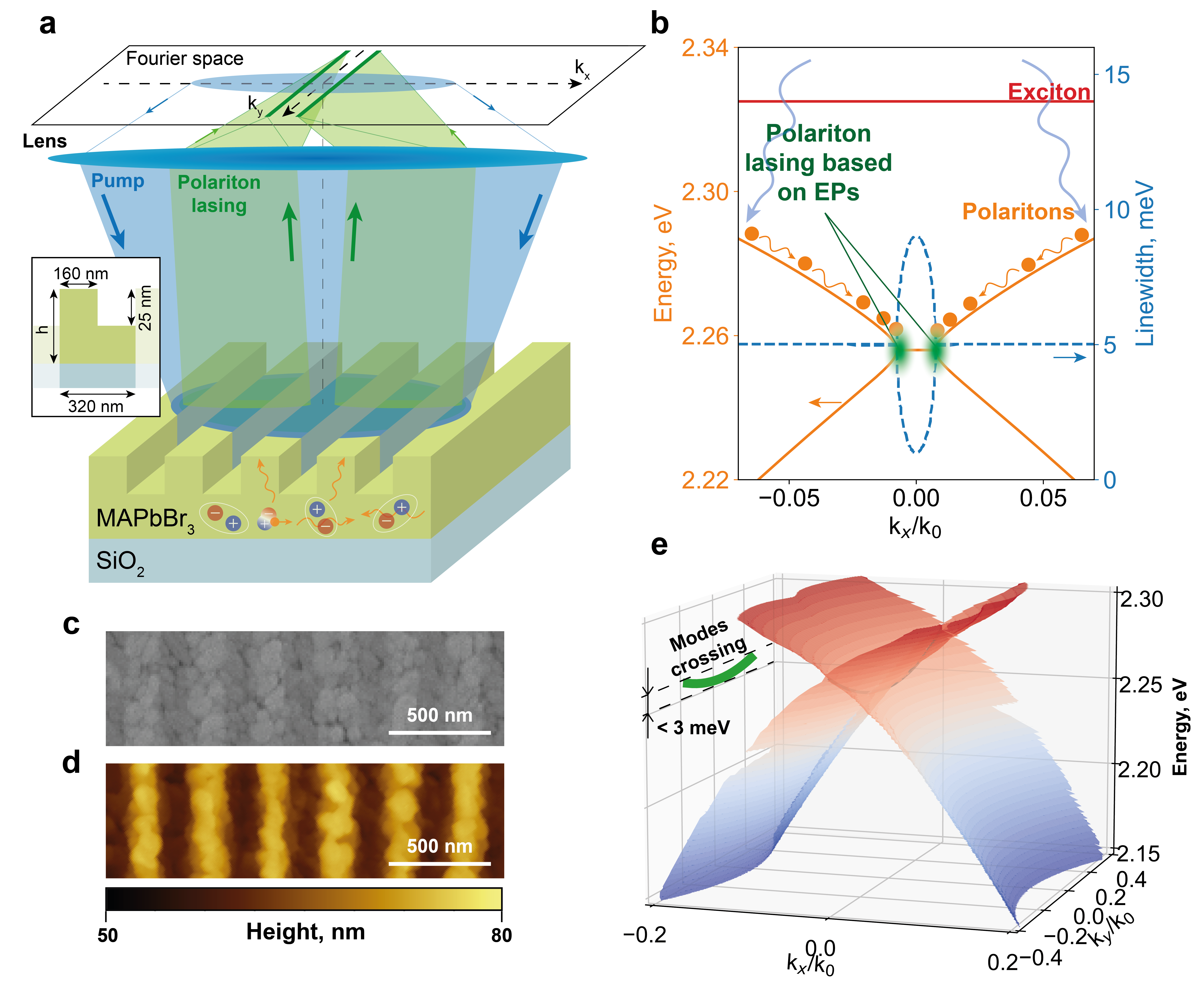
In this work, we experimentally demonstrate room-temperature exciton-polariton lasing in the perovskite non-local metasurface (see the design in Fig. 1a). The polariton lasing is based on the EPs that appear in the spectral vicinity of a symmetry-protected BIC under a non-resonant optical pump in the nonlinear regime (Fig. 1b). The observed lasing emission is characterized by unidirectional propagation along the metasurface periodicity direction and broad distribution along the perpendicular axis in the range of 11 degrees from the normal. Thanks to the dispersion of polariton modes in the perovskite metasurface, the EPs turn into curves in the Fourier plane, resulting in the observed lasing emission directivity.
2 Results
2.1 Fabrication and characterization of the perovskite metasurface
One of the most important advantages of perovskites is the solution methods of synthesis, which provide the low-cost fabrication of these materials and make them very promising for real-world applications.[44] Also, halide perovskites are known as an admirable material for nanoimprint lithography due to their crystal lattice softness, which is also very suitable for further scaling. [35, 45] We use both techniques for the fabrication of MAPbBr3 metasurface, which demonstrate the high quality of the morphology and resulting optical modes (see Methods and Supplementary Information (SI) for details).
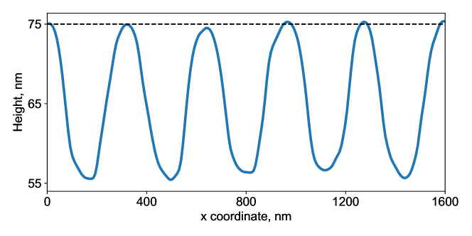
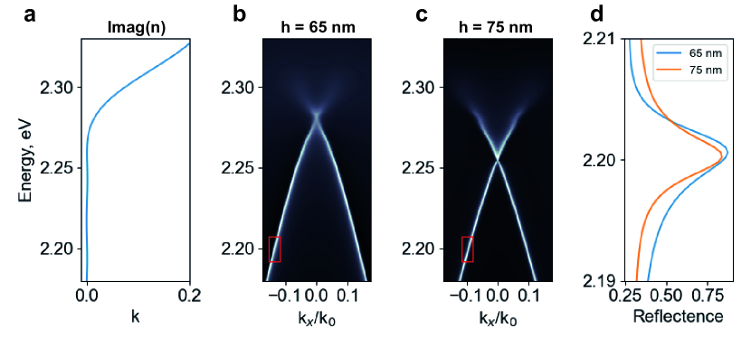
The perovskite metasurface represents a periodic grating, controlled by the mold, with a period of 320 nm, which is determined from the scanning electron microscopy (SEM) image, shown in Fig. 1c. The grating ridge height is around 20 nm, the comb width is around 160 nm, and the full sample thickness from the substrate to the comb top is around 75 nm, according to the atomic force microscopy (AFM) measurements shown in Fig. 1d. The extracted grating profiles along the x-axis are shown in Fig. S2 in SI. We also fabricate the sample with a thickness of 65 nm by increasing the spin-coating rotation speed. It is observed that perovskite grains in the nanoimprinted structure are not deformed or damaged and the resulting structure possesses high crystallinity. According to our observations, due to the room-temperature nanoimprinting process applied during the intermediate phase, the crystallization process continues in the mold geometry during the nanoimprint process. Moreover, after the annealing, the structure stiffens and cannot be modified by the polycarbonate mold at room temperature.
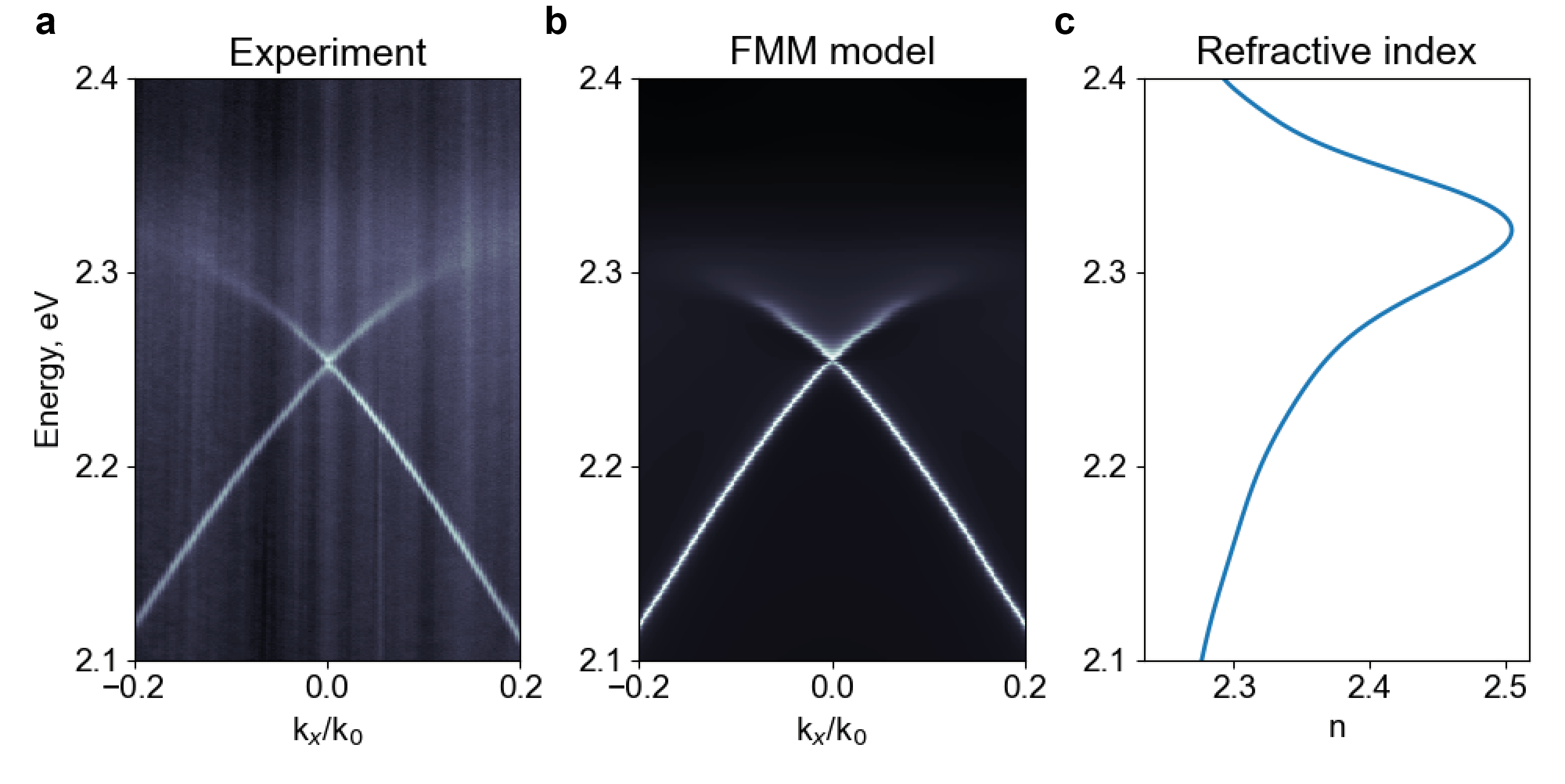
Based on the extracted perovskite non-local metasurface geometry parameters and the MAPbBr3 refractive index, studied before,[46] we estimate the wavevectors of leaky mode resonances with linear polarization co-direct with a groove of metasurface (TE polarization) as a function of the photon energy by the Fourier Modal Method (FMM) [47] for the sample with a thickness of 75 nm. As the estimations well correlate with the experimentally measured angle-resolved reflection spectrum at = 0 (Fig. S3 in SI), we simulate the full dispersion surface of the perovskite metasurface shown in Fig. 1e (see section 1 of SI for details). In the current geometry, the modes with opposite x-components of the group velocities intersect at the curve, located in the plane of = 0. Note that, in the range of , spectral positions of the mode intersection points, shown as a green line in Fig. 1e, vary in the range of 3 meV. As the mode linewidth of 6 meV exceeds this value, the intersection set of points represents a straight line without any energy dependence. Also, the leaky modes are studied in the region of the exciton resonance and, therefore, are affected by it (Fig. S4 in SI). The curvature of the leaky mode at constant from the linear dependence to the exciton resonance asymptote is a sign of exciton-polariton behavior.[48]
2.2 Strong light-matter coupling regime in perovskite metasurface
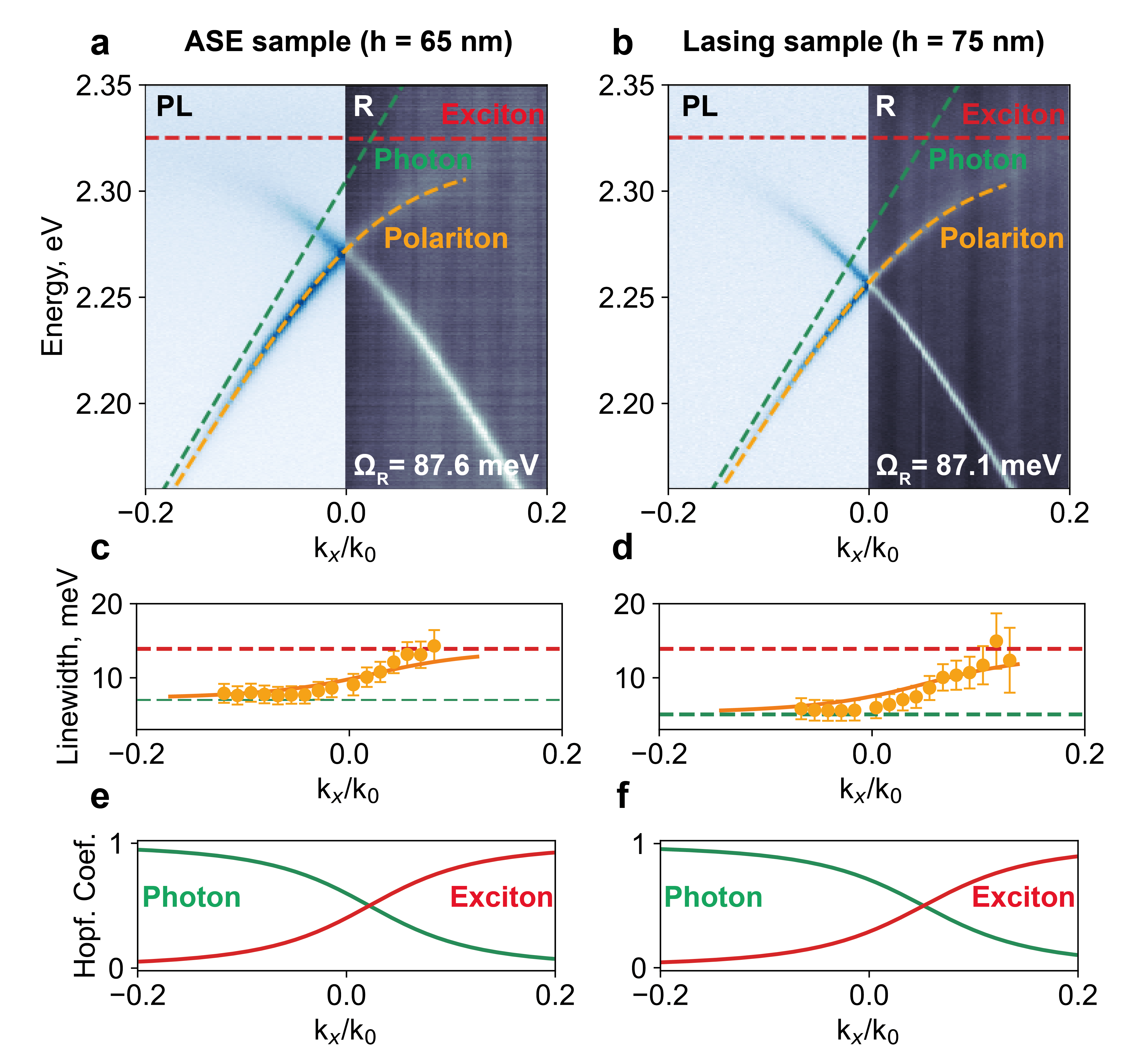
In order to confirm the strong light-matter coupling regime, we perform angle-resolved reflectance and photoluminescence measurements (see Methods for details). The angle-resolved measurements at = 0 in TE polarization are performed for two samples with thicknesses of 65 and 75 nm, but having identical pitch and modulation depth, shown in Figs. 2a and 2b. The samples are labeled as an ”ASE sample” and ”lasing sample”, respectively, as they provide spectrally broad and narrow stimulated emission, respectively, under a non-resonant femtosecond pump. The difference in the sample thickness causes the variation in the real and imaginary parts of leaky modes dispersions (Figs. 2a and 2b) and linewidths (Figs. 2c and 2d). Both dispersions demonstrate the curvature of the mode near the exciton resonance, which is the sign of the exciton-polaritons, as was mentioned above. In the absence of the excitonic resonance, the leaky mode has nearly linear behavior as a function of in the spectral range of interest and can be considered as an uncoupled cavity photon (see Fig. S4 in SI for details). The observed polariton dispersion can be described by the two-coupled oscillator model[48]:
| (1) |
there stands for the complex energy dispersion of the lower polariton branch; and stand for the real and imaginary parts of the exciton resonance, respectively; and stand for the dispersion and linewidth of the uncoupled cavity photon mode, respectively; and stands for the light-matter coupling coefficient. It should be noted, that we do not observe the upper polariton branch due to the strong optical absorption in the spectral region higher than the exciton resonance.[49] Nevertheless, Rabi splitting, which is identified as a difference between lower and upper polariton branches in the intersection point can be estimated as
| (2) |
If the coupling coefficient exceeds the half-difference of the linewidths (i.e., ) and the value of Rabi splitting exceeds the half-sum (i.e., ) strong light-matter coupling regime appears.[48]
In order to estimate the coupling coefficient and check if the system is in a strong light-matter coupling regime, we extract the leaky mode dispersion and linewidths from the measured angle-resolved PL spectra by the fitting of the mode resonances at each by the Lorentz peak function. As uncoupled photon cavity mode dispersion in the metasurface is considered to have linear behavior with respect to the , we estimate it by the linear approximation of the leaky mode in the spectral region far from the exciton resonance (1.9-2.0 eV). The linewidth is estimated from the leaky mode linewidth in the same spectral region and is equal to 7 meV for the ASE sample and 5 meV for the lasing sample. The coupling coefficient is determined as an optimized parameter in the fitting by the two-coupled oscillator model. In the same way, the exciton resonance and linewidth are also determined as optimized parameters and well correspond to the previous estimations.[50, 51] It should be noted that this approach of the exciton level estimation well predicts the exciton resonance in comparison with other methods.[52] The result of the complex mode dispersion fitting by the two-coupled oscillator model is shown in Figs. 2a-d. The real part of the , shown by the dashed lines in Figs. 2a-b well corresponds to the experimental data, as well as the imaginary part shown in Figs. 2c-d. The coupling coefficient is estimated to be equal to 43.8 meV for both samples, but is 87.6 meV for the ASE sample and 87.1 meV for the lasing sample. As the coupling coefficient depends on the material properties and electric field localization, it is the same for both samples, but the difference is in the photon cavity linewidth, which causes the difference in . As for both samples, exceeds the exciton and photon linewidths half-difference, which is around 7 and 9 meV, as well as is larger than the half-sum, which is around 9.5 and 10.5 meV, we confirm that in the studied perovskite metasurface, the strong light-matter coupling regime is achieved.
As exciton-polaritons are hybrid light-matter quasiparticles, there can be estimated a fraction of the exciton and photon in the polariton wavefunction, which is also called Hopfield coefficients (see Section 2 in SI).[48] The estimated coefficients as a function of the are shown in Figs. 2e-f. At the -point, where = 0, the exciton fraction is around 0.4 in the ASE sample and around 0.29 in the lasing sample. On the one hand the higher the exciton fraction, the larger the optical nonlinear effects and exciton optical gain, but on the other hand, with a higher exciton fraction, nonradiative losses rise, which reduces the polariton lifetime. As a result, there exists a balance between these two effects on the polariton branch, where polaritons may efficiently accumulate and cause polariton stimulation in this state after some threshold.[25, 24]
2.3 Polariton-mediated ASE and lasing in perovskite metasurface
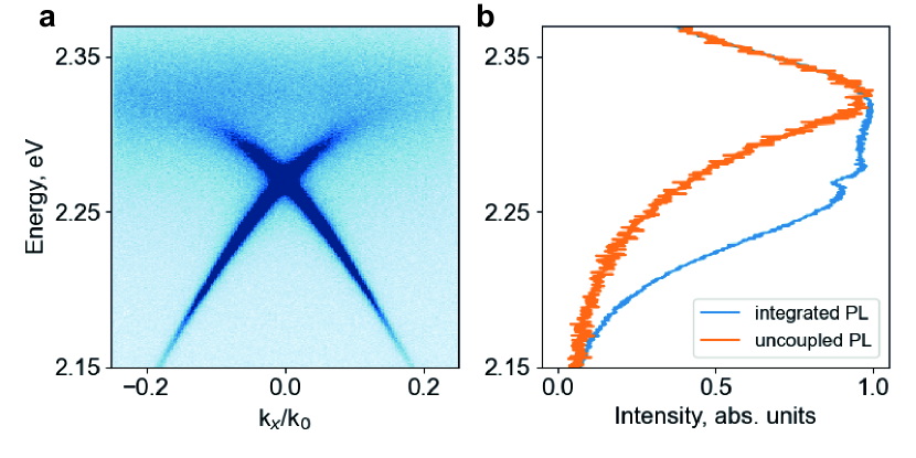
To study the stimulated emission of the samples, we perform angle-resolved PL measurements by varying the pump fluence. Under the pump fluences around 6 J/cm2 and lower we observe linear emission regime, coming from the polariton branches and background PL, which is observed from the unstructured film (Figs. 3a and 3b). The intensity of the background PL spectrum is much lower than the emission intensity of polariton modes and it is hidden in figures, however, it is still noticeable (see Fig. S7 in SI for details). With increasing the pump fluence, we observe a blueshift and broadening of the polariton modes, and after the pump threshold, we observe stimulated emission. In the case of the ASE sample, broad enhanced amplified spontaneous emission (ASE) on the polariton branch for in the range of 0.03-0.05 is observed, where the exciton Hopfield coefficient is around 0.3. But in the case of the lasing sample, we observe spectrally narrow emission with 0, corresponding to the polariton accumulation in EPs. Since the metasurface with a height of 65 nm provides the spectral position of modes crossing closer to the exciton resonance in comparison with 75 nm, the non-radiative optical losses are higher (see SI for details). Also, the radiative losses are increased due to the higher relative modulation (see SI for details). Therefore, the full losses of the optical resonance at cannot be compensated with optical gain to achieve EPs and hence provide only ASE.
With increasing the pump fluence ASE shifts to the red region along the polariton branch and spectrally broadens (Fig. 3a). Meanwhile, the lasing emission increases in intensity, broads, and slightly shift to the blue region (Fig. 3b). The reason for the observed effect is supposed to be in the origin of the polariton relaxation.[25, 27] In the case of the ASE, the accumulated polaritons in a nonlinear regime scatter to the lower energies, as there does not exist a state where a large number of polaritons can be accumulated. However, in the lasing sample, in a nonlinear regime, there appear the specific states at the 0, where the polariton condensation with a narrow lasing emission is achieved. As was mentioned above, the states are supposed to be the EPs, which are caused by the stimulated emission and will be described in detail below.
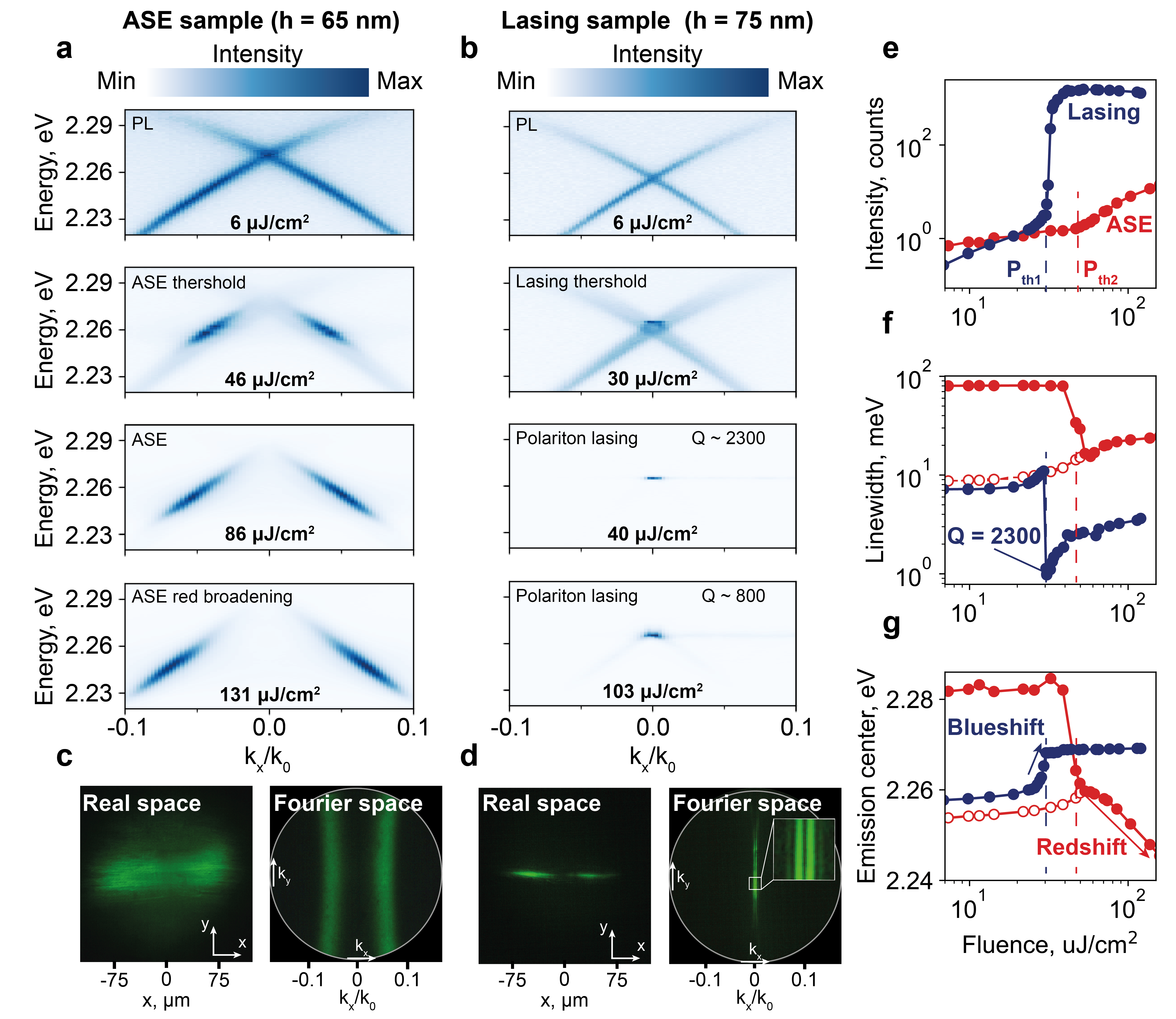
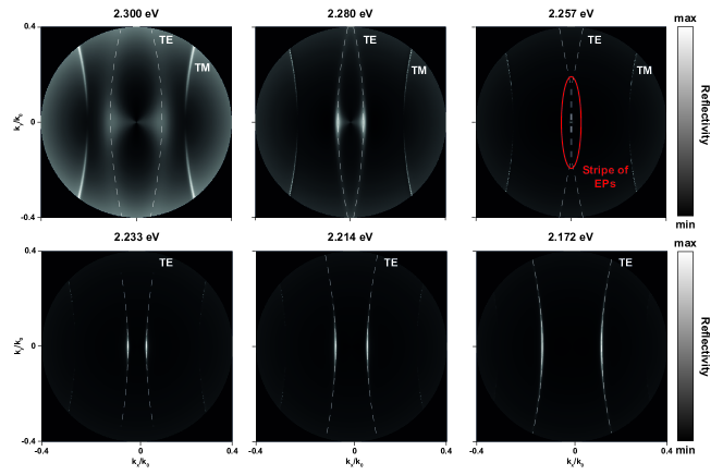
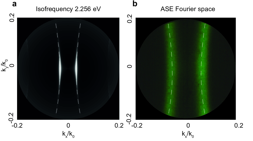
In the real space (Fig. 3c), the ASE emission is characterized as high-intensive spots with speckles on the left and right sides from the pump spot center with a wide distribution over the y-axis. Meanwhile, the lasing emission has a narrow distribution over the y-axis (Fig. 3d). In the Fourier space, ASE is almost uniformly distributed over the polariton branches, showing isofrequency contours in the range of the ASE spectral center (Fig. S6 in SI). However, the lasing emission is localized along the = 0 with almost a straight line with respect to the (see inset in Fig.3d). As was shown before, the spectral position of the modes intersection is considered as a constant for the (Fig. 1e), and therefore EPs are supposed to exist over the whole of this stripe. As a result, polaritons accumulate equiprobably over the stripe and produce the unidirectional lasing. It should be noted that in the Fourier space image of the lasing, we detect a characteristic dip in the lasing intensity exactly around = 0 because of the symmetry mismatching between the BIC and plane wave propagating normally. The EPs appearing in the nonlinear regime are slightly detuned from the = 0. It is not observed in the spectra of the lasing emission, shown in Fig. 3b, because of the limited resolution over , and will be shown further.
In order to analyze the ASE and lasing emission as a function of the pump fluence in detail, we fit it by the Lorentzian function. As ASE is not localized in some , we integrate the emission overall for the analysis (solid red markers in Figs. 3e-g), and for the lasing sample, we study the emission at the = 0 (solid blue markers in Figs. 3e-g). However, in order to compare the mode parameters of the ASE sample before the threshold, we also fit the mode at 0.03, corresponding to the maximum of the ASE at the pump threshold (empty red markers in Figs. 3f-g). Both ASE and lasing emission show the S-curve shape of dependence of the emitted signal intensity as a function of the pump fluence (Fig. 3e). The pump threshold of the ASE is estimated as 46 J/cm2 and of the lasing emission as 30 J/cm2. The difference in the pump threshold is attributed to the different losses of the samples, mentioned above and also the existence of the EPs in the lasing sample. The EPs appear in the system in a nonlinear regime when polariton relaxation provides the optical gain and does not require overcoming all losses (see Section 3 of SI). When it appears, the probability of the polaritons scattering in this state dramatically increases, which reduces the lasing threshold. Also, the lasing sample shows an enhanced increase in the intensity after the threshold by more than three orders of magnitude in comparison with the one order observed in the ASE sample. This can be explained by the dramatically increased rate of polariton stimulation to EPs in the nonlinear regime.[24] The polaritons reaching this state radiatively recombines, producing lasing emission in a time scale much shorter than a non-radiative lifetime,[53] which thus strongly suppresses non-radiative recombination. The slight decrease of the lasing intensity at higher fluence can appear due to the further increase of the optical gain, leading to the disappearance of the polariton mode degeneracy and the fade of the exceptional points. Also, it can be attributed to Auger recombination or additional heating of the material. [54]
The integrated emission of the ASE sample in the linear regime before the threshold represents a broad spectrum with a linewidth around 80 meV and a center around 2.28 eV, as shown in Figs. 3f and 3g by red solid markers. It should be noted that the estimated linewidth here is broadened with respect to the background PL spectrum, because the leaky modes enhance the outcoupled emission in the red region (see Fig. S7 in SI for details). At the threshold, the linewidth rapidly drops to the values of the mode linewidth (shown as red empty markers), as well as the emission center, because the ASE is strongly localized and enhanced by the polariton mode as it is shown in Fig. 3a. It should also be noted that exactly before the threshold the center of the mode slightly shifts to the blue region, which is attributed to the nonlinear polariton blueshift under the non-resonant pump.[16, 6] With increasing the pump fluence, ASE spectrum broadens and shifts to the red region, because of the polariton relaxation discussed above. The lasing sample exhibits the mode linewidth of around 6 meV before the threshold with a spectral center energy of 2.258 eV. With further elevating the pump fluence, the mode shifts to the blue region by a value of 10 meV and broadens due to the polariton-polariton interaction. [45, 52, 6] Around the threshold, narrow lasing emission appears with a linewidth of around 1 meV corresponding to a Q-factor of 2300. With further increasing the pump fluence, the lasing mode broadens and slightly shifts to the blue region. The broadening is supposed to be due to the temporal changing of the lasing center peak during the emission. The blueshift of the lasing peak is determined by the number of polaritons. After the high-intensity pump pulse is absorbed, the formed polaritons shift the polariton branch to the blue region and the lasing emission appears. When the polaritons annihilate, producing the lasing emission, the number of polaritons reduces and the branch starts to return back to its initial spectral position. As a result, we observe broadened integrated-over-time lasing spectra. This assumption was previously confirmed by the temporal resolution of the lasing emission in polariton systems with a streak-camera.[16, 53]
Observation of the EPs in the lasing regime
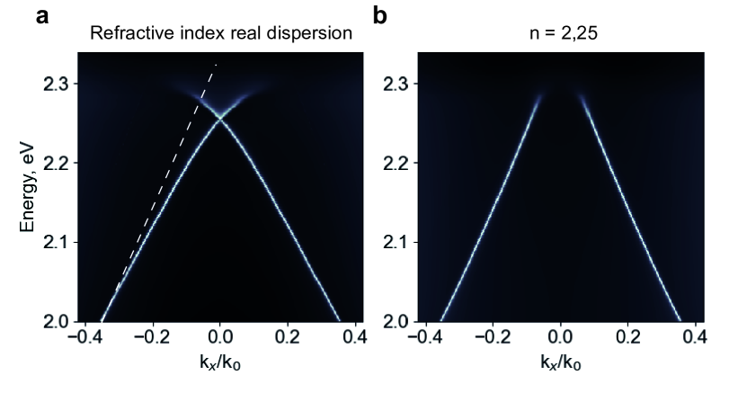
To confirm the presence of the EPs in the stimulated emission of the lasing sample, we increase the magnification of the BFP image, and transferred to the spectrometer imaging CCD to increase the angular resolution over . The angle-resolved spectra with the increased resolution measured for different pump fluences with logarithmic scale in the pseudocolor are shown in Fig. 4a. Under the low pump fluence around 6 J/cm2, we observe a slight enhancement of the spontaneous emission near the = 0, which can be caused by the enhanced spontaneous emission, also reported in ref. [55]. At the pump threshold around 30 J/cm2, polaritons start to interact with each other, which leads to the polariton branch blueshift and polariton stimulated scattering to the lower energies. The latter causes the polariton accumulation in the spectral region of observed ASE and provides the optical gain for leaky modes. As a result, when the critical values of the optical gain are achieved, EPs appear, and we observe two distinguished lasing spots near the = 0 (Fig. 4c). Thanks to the enhanced LDOS, polaritons occupy these states, which leads to the polariton lasing. With increasing the pump fluence, we observe the increase of the lasing peak intensity and then broadening and the blueshift mentioned above (Figs. 4c-d). In the logarithmic scale scattered lasing signals over all are observed, which are attributed to the scattering on the sample impurities and grain boundaries. Also, around fluence 114 J/cm2 it can be observed that the broadened and blueshifted emission preserves the radiation pattern, which is related to the idea of temporal lasing peak broadening discussed above (Fig. 4d).
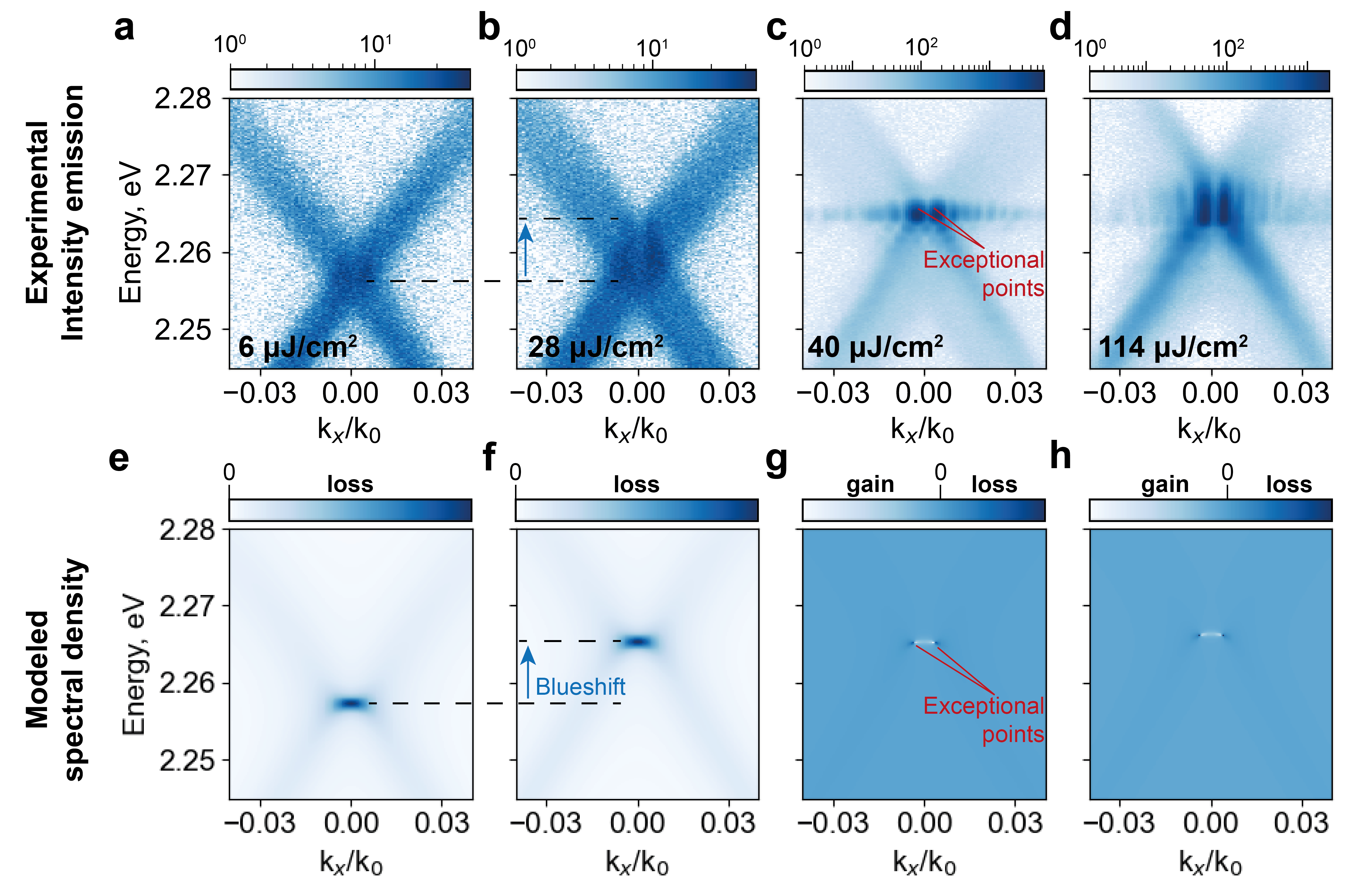
To model the observed phenomena of EPs we calculate the eigenvalues and spectral density of the optical modes, which can be estimated as an imaginary part of Green’s function, identified as , where is the frequency and is the Hamiltonian of the metasurface cavity modes and can be written as: [56, 57, 22]
| (3) |
where stands for the real part of the leaky mode dispersion with positive and negative group velocity, respectively, stands for the non-radiative and radiative losses, respectively, and stands for the coupling coefficients between modes. We extract mode centers and linewidths from the experimental data, shown before. As we do not observe the splitting between two modes at = 0, we take parameter equal to zero. EPs appear in the system when the eigenvalues of the Hamiltonian coalesce:
| (4) |
| (5) |
In this case, spectral density possess artifacts, which are observed in the experiment as lasing points.
The result of the spectral density calculation based on the extracted experimental data in linear regime is shown in Fig. 4e. The ”hotspot” at the -point, where = 0 corresponds to the enhanced spontaneous emission, shown in Fig. 4a. Then, we shift the polariton mode in the model as it is observed in the experiment (Fig. 4f). To take into account the stimulated emission, we assume that the nonradiative losses can be expressed as the difference between absorption (losses) and gain (stimulated polaritons) : . To estimate the we extract the ASE spectrum from the experimental results, shown in Fig. 3a, and consider it as a gain , multiplied by the constant . By varying the parameter we find the critical conditions when the eigenvalues degenerate and EPs appear (see Section 3 of SI for details). After the applying the calculated gain, which does not exceed the full losses, we observe the sign changing of spectral density in the particular places near , which corresponds to the EPs. As EPs are the specific state, which is very sensitive to the variation of the parameters,[17] it has to be destroyed after the higher under higher fluences. However, thanks to the polariton nature, in the regime of the polariton condensation in EPs, all new polaritons which scatter under a higher pump rapidly recombine and do not produce the change of the imaginary part of the mode.
3 Conclusion
In summary, we have demonstrated room-temperature polariton lasing mediated by the EPs in the perovskite-based non-local metasurface. Along with the solution-processable perovskite synthesis methods, the nanoimprint lithography provides large-area gratings supporting high-Q modes (up to Q2300) formed by symmetry-protected BIC and the EPs in the active nonlinear regime. We have revealed that the ASE in the studied samples originates from the accumulation of polaritons in the spectral region with the excitonic fraction in polariton of around 0.3. With further increase of the carrier concentration, the ASE broadens towards the red region due to the polariton relaxation, and EPs appear when the metasurface modes are crossed within the gain spectral range. Our results explain the fundamental origin of the lasing in lead-bromide metasurfaces and open new ways for the realization of room-temperature planar polariton lasers based on a rich variety of halide perovskites. Since the proposed cavity design is close to the most optimal case, we envision further lasing thresholds lowering through the material properties optimization via the synthesis of highly crystalline perovskite films [58, 59, 60] and cation engineering [61], which can lead to the low-cost continuous wave [62, 63] and electrically pumped lasers [64], essential for industrial applications.
4 Experimental Section
Perovskite metasurface fabrication
The fabrication process is divided into three main steps: solution preparation, thin film spin-coating, and nanoimprint lithography. First, the perovskite solution is prepared in the dry N2 glove box by the mixture of 33.59 mg of MABr (TCI) and 110.1 mg of PbBr2 (TCI). Then it is dissolved in a 1 mL mixture of DMF and DMSO in a ratio of 3:1 and steered by a magnetic stirrer for 24 h. Second, substrates of SiO2 are cleaned by consistent sonication in deionized water, acetone, and isopropanol for 10 min. After it is dried out and put into the plasma cleaner for 10 min to achieve high surface adhesion. Cleaned substrates are transferred to the dry N2 glove box, where further film deposition is provided. The perovskite film synthesis starts with the deposition of 30 L MAPbBr3 solution on the cleaned substrate and then the spin-coater starts the rotation. The substrate with a deposited solution is spun for 50 s with a speed rotation of 3.000 or 3.500 rates per minute (rpm), depending on the target film thickness. At the 35th s, after the rotation starts, 300 L of the antisolvent (toluene) is dripped at the top of the rotated substrate to remove the solution and cause fast and uniform film crystallization. The surface morphology, XRD patterns, and absorbance spectrum are in good agreement with previous works [65, 50] and are shown in Figure S11, S12, and S13, respectively, in SI. At the third stage of the synthesis substrate with perovskite film in the intermediate phase before thermal annealing is transferred to a laboratory press for the nanoimprint lithography. The mold for the nanoimprint represents the periodic grating with a period of 320 nm, a comb height of 25 nm, and a ratio between comb width and structure period (FF) of 0.5, made of polycarbonate. The perovskite film with the mold on the top is located in the laboratory press, where the pressure of around 200 MPa is applied for 10 min. After the mold is removed, the substrate with the perovskite imprinted film is annealed at 90 ∘C for 10 min in the atmosphere of the dry N2 glove box.
Angle-resolved spectroscopy
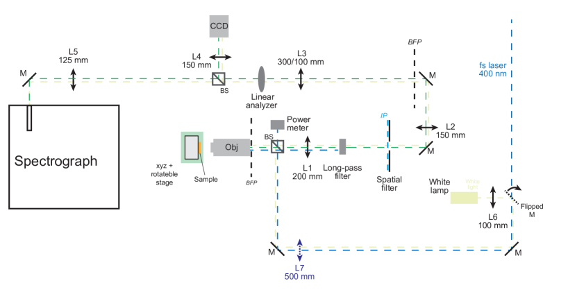
Angle-resolved spectroscopy measurements are performed with a back-focal-plane (BFP) 4f setup by using a slit spectrometer, coupled to the imaging EMCCD camera (Andor Technologies Kymera 328i-B1 + Newton EMCCD DU970P-BVF) and a halogen lamp, coupled to the optical fiber with the collimation lens, employed for the white light illumination. Olympus Plan Achromat Objective with a magnification of 10x and numerical aperture of 0.25 is used for the excitation and collection of the signal. Spatial filtering is carried out in the intermediate image plane (IP), transferred by the 4f scheme. The polarization is filtered by a linear polarizer after the spatial filter. Angle-resolved photoluminescence measurements are performed in the same setup by using the femtosecond (fs) laser with a wavelength of 400 nm and a repetition rate of 1 kHz. The laser system represents mode-locked Ti:sapphire laser at 800 nm, which is used as a seed pulse for the regenerative amplifier (Spectra Physics, Spitfire Pro), and then is frequency-doubled via BBO crystal. A lens with a focal distance of 500 mm is used to focus the laser beam in the BFP to achieve a large pump spot of around 175 m. To filter the laser in the collection channel long-pass filter FEL450 is used. A CCD camera (Thorlabs 1.6 MP Color CMOS Camera DCC1645C) with a 150 mm tube lens after the beamsplitter in the collection channel is used for the imaging of the real and Fourier space. The experimental scheme is shown in Fig. S1 in SI.
Supporting Information
Supporting Information is available from the Wiley Online Library or from the author.
Acknowledgements
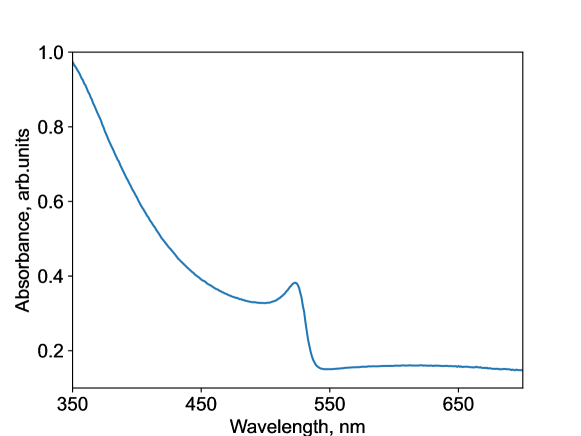
The authors thank Furkan Isik for the provided SEM pictures and absorbance spectra of the samples. The authors also thank Farzan Shabani for the provided XRD pattern measurements. The work was partially done in ITMO Core Facility Center ”Nanotechnologies”. A.K.S. acknowledges the Deutsche Forschungsgemeinschaft (Grant SFB TRR142/project A6), the Mercur Foundation (Grant Pe-2019–0022), and TU Dortmund core funds. This work was also supported by the Ministry of Science and Higher Education of the Russian Federation (Project 075-15-2021-589) and Priority 2030 Federal Academic Leadership Program. H.V.D. acknowledges the support from JUBA.
References
- [1] D. Sanvitto, V. Timofeev, Exciton Polaritons in Microcavities: New Frontiers, volume 172, Springer Science & Business Media, 2012.
- [2] H. Deng, G. Weihs, C. Santori, J. Bloch, Y. Yamamoto, Science 2002, 298, 5591 199.
- [3] J. Kasprzak, M. Richard, S. Kundermann, A. Baas, P. Jeambrun, J. M. J. Keeling, F. Marchetti, M. Szymańska, R. André, J. Staehli, et al., Nature 2006, 443, 7110 409.
- [4] H. Deng, G. Weihs, D. Snoke, J. Bloch, Y. Yamamoto, Proceedings of the National Academy of Sciences 2003, 100, 26 15318.
- [5] C. Weisbuch, M. Nishioka, A. Ishikawa, Y. Arakawa, Physical Review Letters 1992, 69, 23 3314.
- [6] H. Deng, H. Haug, Y. Yamamoto, Reviews of Modern Physics 2010, 82, 2 1489.
- [7] E. Estrecho, T. Gao, N. Bobrovska, D. Comber-Todd, M. D. Fraser, M. Steger, K. West, L. N. Pfeiffer, J. Levinsen, M. Parish, et al., Physical Review B 2019, 100, 3 035306.
- [8] S. Christopoulos, G. B. H. Von Högersthal, A. Grundy, P. Lagoudakis, A. Kavokin, J. Baumberg, G. Christmann, R. Butté, E. Feltin, J.-F. Carlin, et al., Physical Review Letters 2007, 98, 12 126405.
- [9] R. Su, C. Diederichs, J. Wang, T. C. Liew, J. Zhao, S. Liu, W. Xu, Z. Chen, Q. Xiong, Nano letters 2017, 17, 6 3982.
- [10] R. Su, J. Wang, J. Zhao, J. Xing, W. Zhao, C. Diederichs, T. C. Liew, Q. Xiong, Science Advances 2018, 4, 10 eaau0244.
- [11] S. Betzold, M. Dusel, O. Kyriienko, C. P. Dietrich, S. Klembt, J. Ohmer, U. Fischer, I. A. Shelykh, C. Schneider, S. Hofling, ACS Photonics 2019, 7, 2 384.
- [12] K. Koshelev, A. Bogdanov, Y. Kivshar, Science Bulletin 2019, 64, 12 836.
- [13] A. Overvig, A. Alù, Laser & Photonics Reviews 2022, 16, 8 2100633.
- [14] V. Kravtsov, E. Khestanova, F. A. Benimetskiy, T. Ivanova, A. K. Samusev, I. S. Sinev, D. Pidgayko, A. M. Mozharov, I. S. Mukhin, M. S. Lozhkin, et al., Light: Science & Applications 2020, 9, 1 1.
- [15] K. Koshelev, S. Sychev, Z. F. Sadrieva, A. A. Bogdanov, I. Iorsh, Physical Review B 2018, 98, 16 161113.
- [16] V. Ardizzone, F. Riminucci, S. Zanotti, A. Gianfrate, M. Efthymiou-Tsironi, D. Suàrez-Forero, F. Todisco, M. De Giorgi, D. Trypogeorgos, G. Gigli, et al., Nature 2022, 605, 7910 447.
- [17] M.-A. Miri, A. Alù, Science 2019, 363, 6422 eaar7709.
- [18] B. Peng, Ş. K. Özdemir, M. Liertzer, W. Chen, J. Kramer, H. Yılmaz, J. Wiersig, S. Rotter, L. Yang, Proceedings of the National Academy of Sciences 2016, 113, 25 6845.
- [19] T. Goldzak, A. A. Mailybaev, N. Moiseyev, Physical Review Letters 2018, 120, 1 013901.
- [20] I. Doronin, A. Zyablovsky, E. Andrianov, A. Pukhov, A. Vinogradov, Physical Review A 2019, 100, 2 021801.
- [21] A. A. Zyablovsky, I. V. Doronin, E. S. Andrianov, A. A. Pukhov, Y. E. Lozovik, A. P. Vinogradov, A. A. Lisyansky, Laser & Photonics Reviews 2021, 15, 3 2000450.
- [22] L. Lu, Q. Le-Van, L. Ferrier, E. Drouard, C. Seassal, H. S. Nguyen, Photonics Research 2020, 8, 12 A91.
- [23] A. Pick, B. Zhen, O. D. Miller, C. W. Hsu, F. Hernandez, A. W. Rodriguez, M. Soljačić, S. G. Johnson, Optics Express 2017, 25, 11 12325.
- [24] Q. Zhang, T. Krisnanda, D. Giovanni, K. Dini, S. Ye, M. Feng, T. C. Liew, T. C. Sum, The Journal of Physical Chemistry Letters 2022, 13, 31 7161.
- [25] H. Shan, I. Iorsh, B. Han, C. Rupprecht, H. Knopf, F. Eilenberger, M. Esmann, K. Yumigeta, K. Watanabe, T. Taniguchi, et al., Nature Communications 2022, 13, 1 1.
- [26] A. K. Jena, A. Kulkarni, T. Miyasaka, Chemical Reviews 2019, 119, 5 3036.
- [27] Y. Zhang, C.-K. Lim, Z. Dai, G. Yu, J. W. Haus, H. Zhang, P. N. Prasad, Physics Reports 2019, 795 1.
- [28] R. Su, A. Fieramosca, Q. Zhang, H. S. Nguyen, E. Deleporte, Z. Chen, D. Sanvitto, T. C. Liew, Q. Xiong, Nature Materials 2021, 20, 10 1315.
- [29] H. Huang, M. I. Bodnarchuk, S. V. Kershaw, M. V. Kovalenko, A. L. Rogach, ACS Energy Letters 2017, 2, 9 2071.
- [30] R. Su, S. Ghosh, J. Wang, S. Liu, C. Diederichs, T. C. Liew, Q. Xiong, Nature Physics 2020, 16, 3 301.
- [31] Q. Shang, M. Li, L. Zhao, D. Chen, S. Zhang, S. Chen, P. Gao, C. Shen, J. Xing, G. Xing, et al., Nano Letters 2020, 20, 9 6636.
- [32] K. Peng, R. Tao, L. Haeberlé, Q. Li, D. Jin, G. R. Fleming, S. Kéna-Cohen, X. Zhang, W. Bao, Nature Communications 2022, 13, 1 1.
- [33] R. Tao, K. Peng, L. Haeberlé, Q. Li, D. Jin, G. R. Fleming, S. Kéna-Cohen, X. Zhang, W. Bao, Nature Materials 2022, 1–6.
- [34] A. Zhizhchenko, A. Cherepakhin, M. Masharin, A. Pushkarev, S. Kulinich, A. Porfirev, A. Kuchmizhak, S. Makarov, Laser & Photonics Reviews 2021, 15, 8 2100094.
- [35] S. V. Makarov, V. Milichko, E. V. Ushakova, M. Omelyanovich, A. Cerdan Pasaran, R. Haroldson, B. Balachandran, H. Wang, W. Hu, Y. S. Kivshar, et al., ACS Photonics 2017, 4, 4 728.
- [36] J. Feng, J. Wang, A. Fieramosca, R. Bao, J. Zhao, R. Su, Y. Peng, T. C. Liew, D. Sanvitto, Q. Xiong, Science Advances 2021, 7, 46 eabj6627.
- [37] I. A. Al-Ani, K. As’ Ham, L. Huang, A. E. Miroshnichenko, W. Lei, H. T. Hattori, Advanced Optical Materials 2022, 10, 1 2101120.
- [38] K. As’ ham, I. Al-Ani, W. Lei, H. T. Hattori, L. Huang, A. Miroshnichenko, Physical Review Applied 2022, 18, 1 014079.
- [39] N. H. M. Dang, S. Zanotti, E. Drouard, C. Chevalier, G. Trippé-Allard, M. Amara, E. Deleporte, V. Ardizzone, D. Sanvitto, L. C. Andreani, et al., Advanced Optical Materials 2022, 10, 6 2102386.
- [40] S. A. Veldhuis, P. P. Boix, N. Yantara, M. Li, T. C. Sum, N. Mathews, S. G. Mhaisalkar, Advanced Materials 2016, 28, 32 6804.
- [41] N. Pourdavoud, A. Mayer, M. Buchmüller, K. Brinkmann, T. Häger, T. Hu, R. Heiderhoff, I. Shutsko, P. Görrn, Y. Chen, et al., Advanced Materials Technologies 2018, 3, 4 1700253.
- [42] C. Huang, C. Zhang, S. Xiao, Y. Wang, Y. Fan, Y. Liu, N. Zhang, G. Qu, H. Ji, J. Han, et al., Science 2020, 367, 6481 1018.
- [43] A. Palatnik, C. Cho, C. Zhang, M. Sudzius, M. Kroll, S. Meister, K. Leo, Advanced Photonics Research 2021, 2, 12 2100177.
- [44] N. J. Jeon, J. H. Noh, Y. C. Kim, W. S. Yang, S. Ryu, S. I. Seok, Nature Materials 2014, 13, 9 897.
- [45] M. A. Masharin, V. A. Shahnazaryan, F. A. Benimetskiy, D. N. Krizhanovskii, I. A. Shelykh, I. V. Iorsh, S. V. Makarov, A. K. Samusev, Nano Letters 2022, 22, 22 9092.
- [46] M. S. Alias, I. Dursun, M. I. Saidaminov, E. M. Diallo, P. Mishra, T. K. Ng, O. M. Bakr, B. S. Ooi, Optics Express 2016, 24, 15 16586.
- [47] L. Li, JOSA A 1997, 14, 10 2758.
- [48] J. Hopfield, Physical Review 1958, 112, 5 1555.
- [49] N. Sestu, M. Cadelano, V. Sarritzu, F. Chen, D. Marongiu, R. Piras, M. Mainas, F. Quochi, M. Saba, A. Mura, et al., The Journal of Physical Chemistry Letters 2015, 6, 22 4566.
- [50] A. M. Soufiani, F. Huang, P. Reece, R. Sheng, A. Ho-Baillie, M. A. Green, Applied Physics Letters 2015, 107, 23 231902.
- [51] J. Shi, Y. Li, J. Wu, H. Wu, Y. Luo, D. Li, J. J. Jasieniak, Q. Meng, Advanced Optical Materials 2020, 8, 10 1902026.
- [52] M. Masharin, V. Shahnazaryan, I. Iorsh, S. Makarov, A. Samusev, I. Shelykh, arXiv preprint arXiv:2211.04733 2022.
- [53] A. P. Schlaus, M. S. Spencer, K. Miyata, F. Liu, X. Wang, I. Datta, M. Lipson, A. Pan, X.-Y. Zhu, Nature Communications 2019, 10, 1 1.
- [54] L. Lei, Q. Dong, K. Gundogdu, F. So, Advanced Functional Materials 2021, 31, 16 2010144.
- [55] L. Ferrier, P. Bouteyre, A. Pick, S. Cueff, N. H. M. Dang, C. Diederichs, A. Belarouci, T. Benyattou, J. Zhao, R. Su, et al., arXiv preprint arXiv:2203.02245 2022.
- [56] E. Engdahl, E. Brändas, M. Rittby, N. Elander, Journal of Mathematical Physics 1986, 27, 11 2629.
- [57] A. Vijay, H. Metiu, Journal of Chemical Physics 2002, 116, 1 60.
- [58] W. Du, X. Wu, S. Zhang, X. Sui, C. Jiang, Z. Zhu, Q. Shang, J. Shi, S. Yue, Q. Zhang, et al., Nano Letters 2022, 22, 10 4049.
- [59] N. Pourdavoud, A. Mayer, M. Buchmüller, K. Brinkmann, T. Häger, T. Hu, R. Heiderhoff, I. Shutsko, P. Görrn, Y. Chen, H.-C. Scheer, T. Riedl, Adv. Mater. Technol. 2018, 3, 4 1700253.
- [60] Tatarinov, Anoshkin, Tsibizov, Sheremet, Isik, Zhizhchenko, Cherepakhin, Kuchmizhak, Pushkarev, Demir, Makarov, Advanced Optical Materials 2023, 2202407.
- [61] A. L. Alvarado-Leannos, D. Cortecchia, C. N. Saggau, S. Martani, G. Folpini, E. Feltri, M. D. Albaqami, L. Ma, A. Petrozza, ACS Nano 2022.
- [62] Y. Jia, R. A. Kerner, A. J. Grede, B. P. Rand, N. C. Giebink, Nature Photonics 2017, 11, 12 784.
- [63] C. Qin, A. S. Sandanayaka, C. Zhao, T. Matsushima, D. Zhang, T. Fujihara, C. Adachi, Nature 2020, 585, 7823 53.
- [64] T. Wang, Z. Zang, Y. Gao, C. Lyu, P. Gu, Y. Yao, K. Peng, K. Watanabe, T. Taniguchi, X. Liu, et al., Nano Letters 2022, 22, 13 5175.
- [65] Z. Wang, M. Luo, Y. Liu, M. Li, M. Pi, J. Yang, Y. Chen, Z. Zhang, J. Du, D. Zhang, Z. Liu, S. Chen, Small 2021, 17, 25 2101107.
Supplementary Information: Room-temperature exceptional-point-driven polariton lasing from perovskite metasurface
M.A. Masharin A.K. Samusev A.A. Bogdanov I.V. Iorsh H.V. Demir S.V. Makarov*
M.A. Masharin, H.V. Demir
Institute of Materials Science and Nanotechnology and National Nanotechnology Research Center and Electronics Engineering and National Nanotechnology Research Center, Department of Electrical, Department of Physics, Bilkent University, Ankara, 06800, Turkey
M.A. Masharin, A.K. Samusev, A.A. Bogdanov, I.V. Iorsh, S.V. Makarov
ITMO University, School of Physics and Engineering, St. Petersburg, 197101, Russia
Email Address: s.makarov@metalab.ifmo.ru
A.K. Samusev
Experimentelle Physik 2, Technische Universität Dortmund, 44227 Dortmund, Germany
A.A. Bogdanov, S.V. Makarov
Qingdao Innovation and Development Center, Harbin Engineering University, Qingdao 266000, Shandong, China
I.V. Iorsh
Department of Physics, Bar-Ilan University, Ramat Gan, 52900, Israel
H.V. Demir
LUMINOUS! Center of Excellence for Semiconductor Lighting and Displays, School of Electrical and Electronic Engineering, School of Physical and Materials Sciences, School of Materials Science and Engineering, Nanyang Technological University, 639798, Singapore
Calculation of the perovskite PCS isofreqencies and the dispersion surface.
In order to plot the dispersion surface, we calculate isofrequencies of perovskite PCS at different frequencies (energies), shown in Fig. S6. In the range of wavenumbers —— and —— ¡ 0.4 we observe two modes, corresponding to the TE and TM polarizations. TE mode has an electric field codirect with the PCS combs, and TM has a magnetic field co-directed with this direction. In the work, we study only TE mode, as it has stronger electric field localization in the material and therefore is strongly coupled to the exciton resonance. Moreover, in this geometry, only the TE mode has the EPs in the region of optical polariton gain. However, it is possible to achieve EPs in TM geometry with the variation of the sample thickness. We extract the isofreqency curves of TE mode at each energy and assemble them in the one dispersion surface, shown in the main text. It should be noted, that the stripe of the intersection points, which are identified as EPs in the experiment, is observed in calculated FMM isofrequency at 2.257 eV.
The calculated isofrequency of the ASE sample in the spectral region of the ASE emission with measured Fourier plane is shown in Fig. S7. It is shown, that in the experiment the ASE emission is strongly broadened in comparison with the calculation. It is because of the ASE broad spectrum, which contains a broad region of the wavenumbers. Nevertheless, calculated isofreqency in the ASE spectral center well correspond to the experimental observations.
Calculation of the Hopfield coefficients
According to the two-coupled oscillator model the polariton state consists of the exciton and photon with their weights in the wavefunction, depending on the wavevector . The exciton and photon fractions is labeled as and respectively and based on the coupling coefficient can be calculated as [48]
| (6) |
Determination of the optical gain in the EPs model.
The optical gain in the polariton system appears due to the polariton accumulation in the particular state on the polariton branch, where there is an extremum between the scattering probability and the lifetime.[24, 25] However, calculating the optical gain is a challenging task, and therefore we roughly estimate it from the experimental results in order to show qualitatively the origin of EPs. As two of our samples: the ASE sample and the lasing sample are very similar in terms of the mode dispersions, we extract the ASE spectrum, measured from the ASE sample (Fig. S9a). The spectral region of the ASE is in the range of the leaky modes intersection of the lasing sample (Fig. S9b). We assume, that in the lasing sample the spectral region of the polariton accumulation can be considered the same as in the ASE sample. As the spectral position of the mode is connected with we calculate the gain profile in terms of the , as , where is normalized ASE spectrum, extracted from the experimental data and is the amplitude of the gain.
As was described in the main text, we subtract gain profile from the full optical losses: , where is determined as linewidths, extracted from the PL, measured under 6 J/cm2 of pump fluence, shown in Fig.S9c.
| (7) |
With varying of the parameter we calculate real and imaginary parts of the hamiltonian eigenvalues as a function of , shown as dashed blue lines in Fig. S13. We put = 0, as we did not observe the splitting between two modes at the intersection point. To observe the appearance of the EPs we plot the eigenvalues difference of the real and imaginary parts (, ), shown in Fig.S13. In the linear regime, where = 0 we observe the splitting between eigenvalues (Fig. S13a). With increasing we observe that the difference between the real and imaginary parts of eigenvalues starts to decrease (Fig. S13b). At the critical value of , equal to 0.00117, we observe the degeneracy of the eigenvalues, at some particular values of , which are supposed to be the appearance of the EPs (Fig. S13c). Also, EPs are considered a very sensitive state to the environment, and as we also observe, if we increase more, the degeneracy disappears (Fig. S13d).
However, due to the nature of the polariton lasing, we assume, that in the experiment the gain never exceeds the critical value. When the gain achieves the critical value, the EPs polariton condensation state appears there. It means, that all new polaritons in the state promptly recombine, emitting coherent photons. In this polariton system, as described in this work, EPs can be achieved through nonlinear processes of the polariton relaxation, which results in the polariton lasing.