Adsorption-controlled plasma-assisted molecular beam epitaxy of LaInO3 on DyScO3(110): Growth window, strain relaxation, and domain pattern
Abstract
We report the growth of epitaxial LaInO3 on DyScO3(110) substrates by adsorption-controlled plasma-assisted molecular beam epitaxy (PA-MBE). The adsorption-controlled growth was monitored using line-of-sight quadrupole mass spectrometry. In a thermodynamics of MBE (TOMBE) diagram, the experimental growth window was found to be significantly narrower than the predicted one. We found the critical thickness for strain relaxation of the LaInO3 layer (lattice mismatch ) to be of 1 nm using in-situ RHEED analysis. Substrate and film possess an orthorhombic crystal structure which can be approximated by a pseudo-cubic lattice. X-ray-diffraction (XRD) analysis revealed the pseudo-cube-on-pseudo-cube epitaxial relationship of the LaInO3 films to the DyScO3 substrates. This relation was confirmed by transmission electron microscopy (TEM), which further resolved the presence of rotational orthorhombic domains - the majority of which have coinciding -axis with that of the substrate. Raman spectroscopy further confirmed the presence of a LaInO3 layer. Our findings open up the possibility for 2-dimensional electron gases at the MBE-grown heterointerface with BaSnO3.
I Introduction
The family of complex oxides comprises dielectric, semiconducting, superconducting, ferromagnetic, or ferroelectric materials. Their common, perovskite, crystal structure provides the basis for combining these oxides and their respective properties epitaxially to form (multi)-functional heterostructures.
Among these multi functional heterostructures, non-polar SrTiO3 (STO) interfaced with polar perovskites such as LaAlO3[1, 2, 3], LaTiO3[4] or GaTiO3[5, 6] can be considered as the working horse for the evaluation of a 2-dimensional electron gas (2-DEG) realized by a polar discontinuity at the polar/non-polar interface.
However, room-temperature mobilities of these 2-DEGs as well as doped STO films are below 10 cm2/Vs due to the high electron phonon interaction,[6] impeding any possible transistor application.
In search for other suitable channel materials, having the chance for future applications, non-polar La-doped BaSnO3 (BSO) single crystals, with reported room-temperature electron mobilities up to 320 cm2/Vs ,[7] surpassed the mobility values of STO by almost two orders of magnitude. The mobilities achieved in BSO single crystals are also the highest values within the perovskites family up to today, making BSO an excellent channel material for a 2-DEG.[8]
For the realization of such a 2-DEG, polar LaInO3 (LIO) has been predicted to have a conduction band offset of 2.06 eV towards non-polar BSO that can confine a maximum possible 2-DEG electron density of almost 2 per cm2 due to the polar discontinuity at the LIO/BSO interface.[8]
So far LIO single crystals have been grown from the melt,[9] and LIO thin films on lightly La-doped BSO thin films by pulsed laser deposition (PLD). These LIO/BSO:La heterostructures resulted in the formation of a 2-DEG at their interface,[10] but also rotational domains in the LIO film due to the epitaxial mismatch between orthorhombic LIO and cubic BSO.[11]
It is also assumed that the crystal quality is reduced because of the high particle energies in PLD, that cause a higher concentration of point defects such as cation vacancies, interstitials and anti-site defects compared to low energy deposition methods such as molecular beam epitaxy (MBE). [12, 13]
While different flavors of molecular beam epitaxy (MBE) have demonstrated the adsorption-controlled growth of BSO thin films with the highest quality and electron mobility[14, 15, 16], no growth of LIO by MBE has been reported to date.
Here, we demonstrate the adsorption-controlled growth of LIO thin films by plasma-assisted MBE on DyScO3 (DSO) (110) substrates. The growth window, lattice-mismatch-related layer relaxation, and rotational domain pattern are discussed.
II Basic considerations
| LIO | LIO / | |
|---|---|---|
| DSO | -3.93 | -4.33 |
| DSO | -4.04 | -4.46 |
II.1 Crystal structure
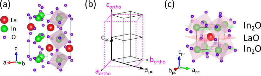
As shown in Fig. 1(a), LIO possesses an orthorhombic unit cell with lattice parameters nm, nm, and nm.[9] The In atoms are surrounded by oxygen atoms in a tilted octahedral arrangement. LIO forms a coinciding (100)-oriented pseudo-cubic (pc) unit cell in its orthorhombic (110)- and (001)-orientation as schematically shown in Fig. 1(b). The lattice constants = 0.41234 nm, and = 0.41072 nm represent the pc orientations (100), (010), and (001), respectively. In addition, the angle between and of 87.6∘ deviates from the 90∘ of an exact cube.[11] Note, that for multiple unit cells, and can be assumed to be identical and are therefore summarized into . Depending on the orientation of the c direction, three different rotational domains contribute to the same cubic 100 orientation. A detailed discussion of the octahedral arrangement of the LIO with respect to a single unit cell and its domain pattern on cubic BSO(100) is given elsewhere.[11] As shown in Fig. 1(c), the pc cell of LIO still results in an alternating stacking of polar LaO (+1) and InO2 (-1) planes due to the charge transfer of 0.5 electrons per unit cell from the LaO to the InO2 below and above.[8]
DyScO3 (DSO) also possesses an orthorhombic crystal structure with lattice constants = 0.5442417 nm, = 0.5719357 nm, and = 0.7904326 nm,[17] which allows for a definition of a pc unit cell with = 0.39475 nm, and = 0.39522 nm. Since we grow our LIO films on DSO(110) substrates, the DSO surface is spanned by and . There are three possible orientations of LIO to grow pc-on-pc on the DSO(110) (one with in out-of-plane and two variants with in out-of-plane direction, but in-plane rotated with respect to each other by 90 The calculated lattice mismatches of the LIO film to the DSO substrate with respect to the possible orientations of the pc cells are shown in Tab. 1, and suggest compressive strain in all cases.
For the following discussion and analysis of the samples, the pc notation is indicated by the subscript "pc" whereas no subscripts are used in the orthorhombic notation.
II.2 Adsorption-controlled growth and TOMBE diagram
Possessing two different cations (A and B), a common challenge for the MBE-growth of complex oxides (ABO3) is the realization of the proper A:B-cation stoichiometry of 1:1. As long as one cation can desorb from the film surface at a given growth temperature, the film stoichiometry can self-adjust as the adsorption of this cation is controlled by the flux of the other cation, the O-flux, and the thermodynamically stable film composition. Suboxides provide an additional desorption channel that enables adsorption-controlled growth even for cations with prohibitively-low vapor pressure, since suboxides often have a significantly higher vapor pressure than their parent cations. The related suboxides can be formed either at the source [18, 19] or intermediately at the growth front.[20] This "adsorption-controlled" approach has been used, for example, to grow BaSnO3. [14, 21]
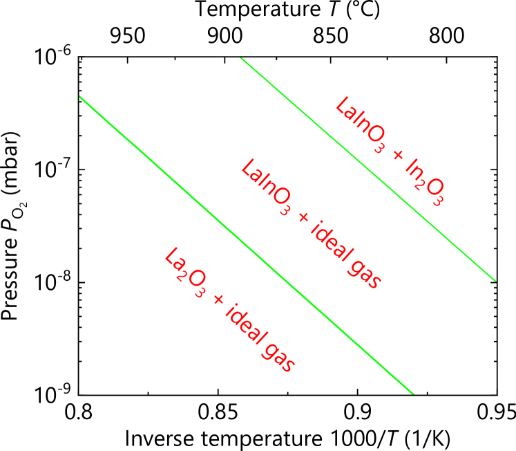
In the case of LIO, the low vapor pressures of La (and its suboxide LaO) result in a sticking coefficient of unity at the growth temperatures accessible to us, whereas In (and its suboxide In2O) possess a high-enough vapor pressure to grant desorption from the growth surface.[19] To delineate the growth conditions that provide an LIO film free of any secondary solid La2O3 or In2O3 phases, a TOMBE diagram shown in Fig. 2 was computed using the FactSage™ thermochemical software package.[22] Such a diagram has been introduced by Nair in the context of adsorption-controlled MBE of ruthenates,[23] and shows the formed solid phases as function of temperature and oxygen partial pressure. For the calculation of the LIO phase, the heat capacity , with , , and [in J/(mol K)], and formation enthalpy kJ/mol of bulk LIO were determined experimentally.[24] The values were added to the FactSage™-database. The TOMBE diagram was calculated assuming an In excess and for an oxygen pressure of 10-6 mbar to match our MBE conditions in terms of In-flux and O2 background pressure. The three different regions in the diagram can be explained as follows: (I) at low temperatures or high oxygen pressures In2O3 is formed next to LaInO3 due to the chosen In excess. (II) at higher temperatures or lower oxygen pressures no In2O3 is formed and the In2O suboxide desorbs from the surface leaving solid LaInO3 behind due to its lower formation enthalpy. (III) at very high temperatures, also the LaInO3 is decomposed and La2O3 is formed.
III Experimental methods
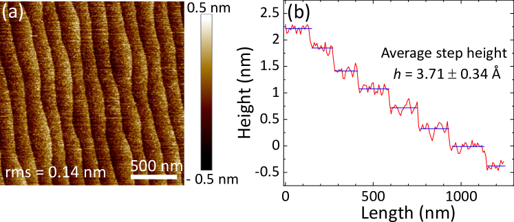
We grew the LIO films on DSO(110) substrates from CrysTec GmbH [(100) oriented]. The DSO substrates were annealed in a quartz tube furnace at 1050∘C for 6 h in flowing oxygen gas at atmospheric pressure [O2 flux at 250 standard cubic centimeters per minute (sccm)] in order to achieve a well defined surface. Fig. 3(a) shows an AFM image of the annealed DSO surface reflecting the unintentional offcut of the wafer. The height profile of the step terrace structure in Fig. 3(b) reveals monolayer steps, indicating single site terminated surface for the subsequent LIO growth. We assume that this site is ScO2 (B-site) according to the chosen annealing parameters.[25] All samples were grown using an rf-plasma source operated at 200 W and used O2 flow rates ranging from 0.07 - 0.14 sccm which corresponds to an oxygen partial pressure of 2.2 Torr in the growth chamber. In order to keep the plasma ignited at low oxygen fluxes, 0.2 sccm Ar were added to the gas flow using a second mass-flow controller, a method previously demonstrated by Tolstova [26] The La and In cell temperatures of = 1550C and = 700C result in beam equivalent pressure (BEP) values of 3 and mbar, respectively, measured by a nude ion gauge at the substrate position without oxygen flux. Under these conditions, the derived La flux of cm determines the growth rate of 1.1 nm/min, while In is provided in excess with a flux of cm. The substrate temperature (925∘C if not indicated otherwise) was measured by a pyrometer.
The surface of the samples during growth was analysed by reflection high energy electron diffraction (RHEED) at an electron energy of 20 keV. The RHEED images were recorded by CCD camera with a resolution of 1024x1024 pixel. Further, a quadrupole mass spectrometer (QMS), that is mounted line-of-sight to the substrate, monitors species that desorb from the sample surface.
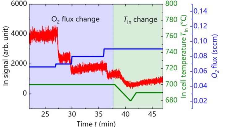
Fig. 4 shows the desorbing In2O-flux (measured as Indium fragment) by line-of-sight QMS. In the blue shaded region, the desorbing In flux decreases with increasing O-flux, as expected from the TOMBE diagram, indicating adsorption control by the O-flux. In the green shaded area, the In signal follows the In cell temperature since less In is being desorbed when less In is provided.
The samples were investigated by atomic force microscopy (AFM) using a Dimension Edge AFM from Bruker in the peak-force tapping mode, and by X-ray diffraction (XRD) with a X’pert pro MRD from Philips PANalytical using a 1 mm detector slit. High-resolution Scanning transmission electron microscopy (STEM) was performed with FEI Titan 80-300 operating at 300 kV and equipped with a Fischione high-angle annular dark-field detector (HAADF) and a highly brilliant cathode (X-FEG). The semi-convergence angle was tuned to 9 mrad and the semi-acceptance angle of the detector was set to 35 mrad. Cross-sectional TEM samples were prepared along the (10) [(010)] lattice direction of the DSO substrate by tripod polishing and argon ion-milling at liquid nitrogen temperature. Ar+ ion-milling was done by a precision ion polishing system (PIPS) at beam energies from 4.0 to 0.2 keV
The Raman spectroscopic measurements were performed in the backscattering configuration at room temperature using the intracavity frequency-doubled output of an Ar+ ion laser at 244 nm (5.08 eV) for optical excitation. The incident laser light was focused by a microscope objective onto the sample surface. The backscattered light was collected by the same objective, spectrally dispersed by an 80-cm spectrograph (LabRam HR Evolution, Horiba/Jobin Yvon) and detected by a liquid-nitrogen-cooled charge-coupled device (CCD) without analysis of the polarization.
IV Results and Discussion
IV.1 Strain relaxation in LIO films
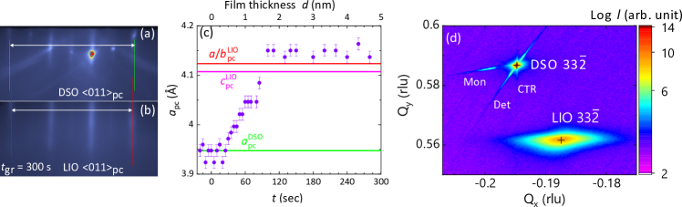
The growth of LIO on DSO was monitored by RHEED. Fig. 5(a) and 5(b) show the <011> azimuth of the DSO(100) substrate and the nominal LIO(100) layer after 300 seconds, respectively. The LIO in-plane lattice parameter was calculated from the analysis of the RHEED patterns [i.e. measuring the distance between the streaks as shown in Fig. 5(a) and 5(b), which is inversely proportional to the in-plane lattice parameter] in order to follow the strain relaxation of the LIO films on DSO. In Fig. 5(c) we see an increase of the lattice parameter after 30 seconds ( 1 monolayer) of film growth from the DSO lattice constant (solid green line) towards the expected LIO lattice constant (solid red line). After 2 nm of LIO growth the determined lattice constant indicates a fully relaxed LIO film. Such a relaxation after 1 nm of film growth or less is also known from BSO films that were grown on SrTiO3 substrates.[16]
A reciprocal space map (RSM) of the 33 reflection of a 200 nm thick LIO film on a DSO substrate is shown in Fig. 5(d). The black crosses mark the theoretically expected position of the DSO and LIO reflections indicating a fully relaxed LIO layer despite the broadened LIO peak in agreement with RHEED analysis.
IV.2 LIO growth window
For the determination of the growth window, we evaluated the RHEED patterns, AFM images, and XRD diffractograms as a function of oxygen flux.
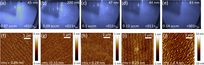
Fig. 6(a)-(e) show RHEED patterns of the LIO(100) surface along the <011> (a)-(d) and <001> (e) azimuth obtained at the final film thickness as indicated. For oxygen fluxes between 0.09 and 0.12 sccm, a streaky RHEED pattern with 1’st and 2’nd Laue circles can be observed whereas for 0.07 and 0.14 sccm a more pronounced intensity modulation of the streaks in the RHEED patterns indicates the transition to three dimensional growth. Note that Fig. 6(e) shows the RHEED pattern along the <001> azimuth since along this direction the effect of the intensity modulation of the streaks is more pronounced than in <011> direction. Fig. 6(f)-(j) show the corresponding AFM images of the LIO surface. For the samples grown at 0.09, 0.1 and 0.12 sccm the surface shows the step terrace structure of the underlying substrate even for a 200 nm thick LIO film [Fig. 6(g)] and root mean square (rms) values in the range of 0.25 - 0.53 nm. Also for the films grown at 0.07 and 0.14 sccm the terrace structure of the substrate still seems to have an influence on the growth of the LIO film. The rms values of 0.89 and 2.4 nm, however, are significantly higher than for the other samples.
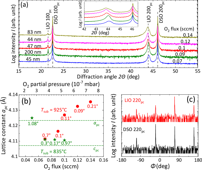
In Fig. 7(a) the symmetric 2 - XRD scan (using a 1 mm detector slit) along the out-of-plane direction reveals the successful growth of LIO for all applied fluxes. No additional phases (e.g., In2O3 or La2O3) were observed within the detection limit of XRD. Solely for a LIO film grown at significantly lower substrate temperature of 730C and = 7.8 mbar, an additional phase was observed (not shown). We identified this phase as In2O3 by its 222 reflection in agreement with the predicted In-rich regime in Fig. 2.
The thickness of the LIO films was determined by the Laue fringes of the LIO 200 reflection shown in the inset for thin films and extrapolated to thicker films assuming the same growth rate for all films. Further, the inset of Fig. 7(a) reveals a shift of the 200 peak position towards lower angles with increasing oxygen flux. Consequently, the derived out-of-plane lattice constants of the LIO films with respect to the oxygen flux in the pc notation shown in Fig. 7(b) (indicated by red squares) also increase with increasing oxygen flux. However, when growth conditions such as substrate temperature are changed (as it was done for the samples labelled by green asterisks), no shift of the lattice constant is observed.
As it will also be shown in the section IV.3, the presence of rotational domains allow for an upper and lower boundary of expected LIO lattice constants assuming total orientation (upper boundary) or total orientation (lower boundary) of the LIO films as indicated by the green dashed lines in Fig. 7(b).
However, due to the use of the 1 mm slit on the detector size, the out-of-plane lattice constants of the samples shown in Fig. 7(b) can only be determined to a value of 4.12 Å with an uncertainty of 0.01 Å. For higher precision of the LIO lattice constant, and for a statement on the preferred domain formation as a function of oxygen, high-resolution XRD would be necessary.
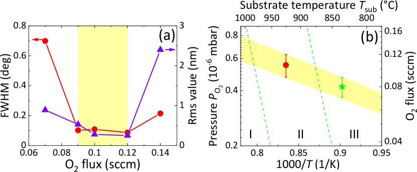
An empirical growth window at a fixed = 925 C was determined by identifying the range of oxygen flux that minizes both, the FWHM of the LIO 200 XRD -rocking curve and the rms surface roughness of the LIO layer. Both these quantities are shown in Fig. 8(a) as red discs (XRD) and purple triangles [roughness determined from the AFM images shown in Fig. 6(f) - (j)]) and the yellow shaded area marks the growth window. The LIO 200 FWHM values in the range of 0.09∘ - 0.15∘ are higher by a factor of 2 - 3 compared to the ones achieved for BSO [14], likely related to the presence of the rotational domains of the pc lattice (see discussion in section IV.3).
In Fig. 8(b) the experimentally derived growth windows at two different of 925C and 835C are indicated by the error bars of the data points. Consequently, the LIO growth window can be extrapolated through the data points as indicated by the yellow shaded area.
The derived LIO growth window as function of substrate temperature and oxygen flux is strikingly different from the predicted TOMBE diagram indicated by the green dashed lines.
IV.3 Epitaxial relation, domain structure, and dislocations of the LIO films
The -scan along the DSO and LIO 220 reflection shown in Fig.7(c) in addition to the coinciding 200 reflections of LIO film and DSO substrate [Fig.7(a)] reveals the pc-on-pc epitaxial relation between DSO and LIO.
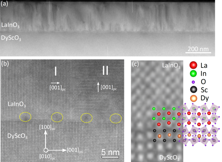
To get a better understanding on the rotational domains of the the orthorhombic structure, that we cannot resolve by XRD, TEM investigations on the sample grown at 0.09 sccm and 925C were performed. Fig. 9(a) shows a STEM HAADF overview of the layer. The layer is characterised by a high density of dislocations, visible as brightness variations under the imaging conditions used here. They start at the interface and penetrate the layer. At higher magnification, the misfit dislocations can be directly seen at the interface [marked by yellow circles in the Fig. 9(b)]. The measured spacing of 8.9 nm between two misfit dislocations corresponds well with the expected dislocation density for the mismatch between DSO and LIO in the given orientation, and for full relaxation (in agreement with our RHEED observations and RSM). A closer look at Fig. 9(b) shows the layer to consist of domains, revealed by the specific contrast pattern. The contrast patterns labelled I and II correspond to LIO domains with and , respectively, parallel to the surface normal of the (100) oriented DSO substrate as described in work by Zupancic et al. [11] for LIO grown on BSO. The formation of differently oriented domains have also been observed in orthorhombic SrRuO3 and CaRuO3 films on cubic substrates.[28, 29]
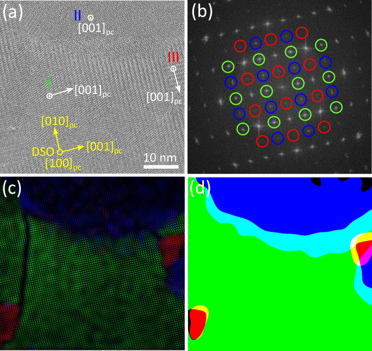
For a statistical analysis of the different LIO domains, we analyze the plan-view sample. Fig. 10(a) shows a part of the analyzed LIO surface along the (100) surface normal of the DSO substrate. Different domain orientations, labelled I, II, and III are marked with green, blue and red, respectively. Domain II (blue) corresponds to parallel to the surface normal of the DSO substrate, whereas domain I (green) and III (red) indicate out-of-plane oriented LIO with parallel and perpendicular, respectively, to of the DSO substrate. To make different orientations distinguishable, we perform Bragg filtering as described in Zupacic [11] using fast Fourier transformation [Fig. 10(b)]. In this way, each filtered image shows only domains with the same orientation [Fig. 10(c)]. After binarization of filtered images, we extract the percentage of each orientation. To better visualize this, we show in Fig. 10(d) an RGB image combined of the processed binary images. In total, a sample area of 0.12 m2 was analyzed. Our analysis shows that oriented domains with coinciding directions of substrate and film (I, green) cover 78.0 ± 9.5 of the surface, while those rotated 90∘ (III, red) cover only 0.2 ± 0.4. The oriented domains (II, blue) occupy 21.8 ± 9.5 of LIO film.
Our findings indicate a strong preference for the alignment of the c-axis of orthorhombic LIO film to that of the orthorhombic DSO(110) substrate (domain I, green color) whereas the LIO domain with c-axis rotated in plane by 90∘ (domain III, red color) is almost completely suppressed. The derived domain distribution differs distinctly from that of orthorhombic LIO grown on cubic BSO, where the three domains are more evenly distributed.[11] Even though our results are not in agreement with lowest strain values listed in Tab. 1, an impact of the orthorhombic substrate on the domain distribution is assumed.
IV.4 Raman spectroscopy
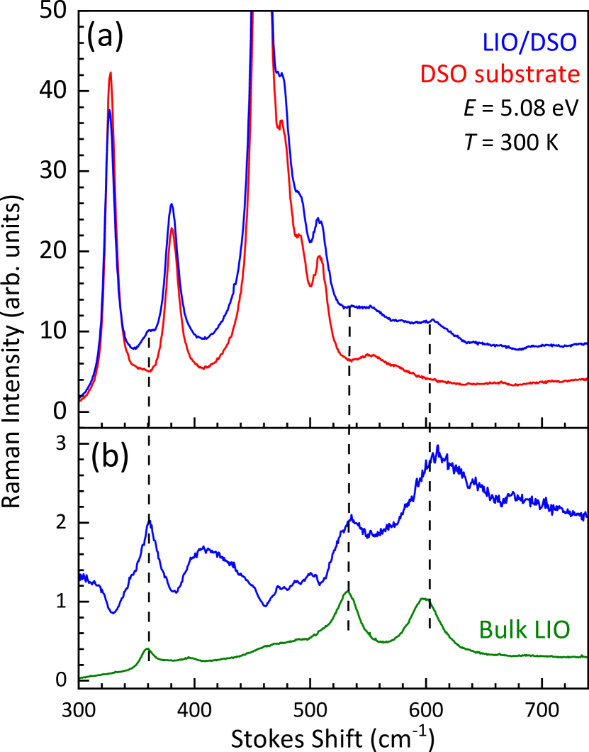
The Raman spectrum of a 100 nm thick LIO film grown on a DSO(100) substrate is shown in Fig. 11(a) together with the spectrum of a bare DSO substrate. Despite the optical excitation (at 5.08 eV) clearly above the optical bandgaps of LIO (4.35 and 4.39 eV, see Ref. [9]), the optical probing depth in the LIO/DSO sample is large enough to result in a dominating Raman signal from the DSO substrate. In order to extract more clearly the contributions of LIO from the LIO/DSO spectrum, we divided the latter one by the one from the DSO substrate.[30] The resulting ratio spectrum is shown in Fig. 11(b) together with the spectrum of a bulk LIO 100 sample recorded under the same conditions. We have detected the same major Raman peaks around 360, 535, and 600 cm-1 for bulk LIO with different surface orientations, however, with somewhat different relative intensities. In fact, the ratio spectrum exhibits three Raman peaks which coincide with those of bulk LIO and have about the same peak widths. This finding confirms the growth of orthorhombic LIO films on DSO substrates under the chosen growth conditions with a crystal quality comparable to that of melt-grown bulk crystals. Note that the identification of the LIO Raman modes for the grown LIO film is rather challenging due to the used DSO substrate. Therefore, for future Raman studies, the use of other substrates is recommended.
V Summary and conclusion
In summary, we have grown LIO thin films on DSO(110) substrates by PA-MBE. Measurements of the desorbing flux as function of growth parameters confirms an adsorption-controlled growth regime, that allows desorption of excess In. A TOMBE diagram for the growth has been theoretically derived. The experimentally determined growth window for high-quality LIO as function oxygen flux for two different substrate temperatures was found to only qualitatively agree with that of the TOMBE diagram. XRD, TEM, and Raman spectroscopy confirmed the formation of an epitaxial LIO film. RHEED, XRD, and TEM show, that the lattice mismatch on the order of -4 resulted in a film relaxation within the first 2 nm by the formation of misfit dislocations at the LIO/DSO interface, as well as threading dislocations that penetrate the entire LIO film. While both substrate and film are orthorhombic, their epitaxial relation is shown to be pc-on-pc with 90∘ rotational domains of the film. In contrast to LIO films grown on BSO with quite evenly distributed rotational domains,[11] the majority of the LIO domains in the present work have a coinciding orthorhombic -axis with that of the DSO substrate (both oriented in-plane) while also domains with -axis oriented out-of-plane are present. It is assumed that 001 oriented substrates with a smaller lattice mismatch may lead to a reduction of rotational domains [31] as well as shutter controlled layer-by-layer growth that in general has been demonstrated to lead to higher crystal quality.[32, 33, 34, 35, 36] The present work paves the way for the formation of polarization-discontinuity-doped 2-DEGs with high room temperature electron mobility in LIO/BSO heterostructures grown by MBE.
Acknowledgements.
We thank Zbigniew Galazka for providing the LIO substrates, Hans-Peter Schönherr and Steffen Behnke for technical support, and Dr. Philipp John and Dr. Jutta Schwarzkopf for critically reading the manuscript. This work was performed in the framework of GraFOx, a Leibniz-ScienceCampus partially funded by the Leibniz association. G.H. and M.Z. gratefully acknowledge financial support from the Leibniz association under Grant No. K74/2017.Data Availability
The data that support the findings of this study are available from the corresponding author upon reasonable request.
References
- Janotti et al. [2012] A. Janotti, L. Bjaalie, L. Gordon, and C. G. Van de Walle, Controlling the density of the two-dimensional electron gas at the SrTiO3/LaAlO3 interface, Phys. Rev. B 86, 241108 (2012).
- Mannhart et al. [2008] J. Mannhart, D. Blank, and H. Hwang, Two-Dimensional Electron Gases at Oxide Interfaces, MRS BULLETIN 33, 10.1557/mrs2008.222 (2008).
- Ohtomo and Hwang [2004] A. Ohtomo and H. Y. Hwang, A high-mobility electron gas at the LaAlO3/SrTiO3 heterointerface, Nature 427, 423 (2004).
- Ohtsuka et al. [2010] R. Ohtsuka, M. Matvejeff, K. Nishio, R. Takahashi, and M. Lippmaa, Transport properties of LaTiO3/SrTiO3 heterostructures, Appl. Phys. Lett. 96, 192111 (2010).
- Moetakef et al. [2011] P. Moetakef, T. A. Cain, D. G. Ouellette, J. Y. Zhang, D. O. Klenov, A. Janotti, C. G. Van de Walle, S. Rajan, S. J. Allen, and S. Stemmer, Electrostatic carrier doping of GdTiO3/SrTiO3 interfaces, Appl. Phys. Lett. 99, 232116 (2011).
- Mikheev et al. [2015] E. Mikheev, B. Himmetoglu, A. P. Kajdos, P. Moetakef, T. A. Cain, C. G. Van de Walle, and S. Stemmer, Limitations to the room temperature mobility of two- and three-dimensional electron liquids in SrTiO3, Appl. Phys. Lett. 106, 062102 (2015).
- Kim et al. [2012] H. J. Kim, U. Kim, H. M. Kim, T. H. Kim, H. S. Mun, B.-G. Jeon, K. T. Hong, W.-J. Lee, C. Ju, K. H. Kim, and K. Char, High Mobility in a Stable Transparent Perovskite Oxide, Appl. Phys. Express 5, 061102 (2012).
- Krishnaswamy et al. [2016] K. Krishnaswamy, L. Bjaalie, B. Himmetoglu, A. Janotti, L. Gordon, and C. G. Van de Walle, BaSnO3 as a channel material in perovskite oxide heterostructures, Applied Physics Letters 108, 10.1063/1.4942366 (2016).
- Galazka et al. [2021] Z. Galazka, K. Irmscher, S. Ganschow, M. Zupancic, W. Aggoune, C. Draxl, M. Albrecht, D. Klimm, A. Kwasniewski, T. Schulz, M. Pietsch, A. Dittmar, R. Grueneberg, U. Juda, R. Schewski, S. Bergmann, H. Cho, K. Char, T. Schroeder, and M. Bickermann, Melt Growth and Physical Properties of Bulk LaInO3 Single Crystals, Phys. Status Solidi A 218, 2100016 (2021).
- Pfützenreuter et al. [2022] D. Pfützenreuter, S. Kim, H. Cho, O. Bierwagen, M. Zupancic, M. Albrecht, K. Char, and J. Schwarzkopf, Confinement of Electrons at the LaInO 3 /BaSnO 3 Heterointerface, Adv Materials Inter 9, 2201279 (2022).
- Zupancic et al. [2020] M. Zupancic, W. Aggoune, T. Markurt, Y. Kim, Y. M. Kim, K. Char, C. Draxl, and M. Albrecht, Role of the interface in controlling the epitaxial relationship between orthorhombic LaInO3 and cubic BaSnO3, Phys. Rev. Materials 4, 123605 (2020).
- Nunn et al. [2021] W. Nunn, T. K. Truttmann, and B. Jalan, A review of molecular-beam epitaxy of wide bandgap complex oxide semiconductors, Journal of Materials Research 10.1557/s43578-021-00377-1 (2021).
- Schmid et al. [2009] M. Schmid, C. Lenauer, A. Buchsbaum, F. Wimmer, G. Rauchbauer, P. Scheiber, G. Betz, and P. Varga, High Island Densities in Pulsed Laser Deposition: Causes and Implications, Phys. Rev. Lett. 103, 076101 (2009).
- Paik et al. [2017] H. Paik, Z. Chen, E. Lochocki, H. Ariel Seidner, A. Verma, N. Tanen, J. Park, M. Uchida, S. Shang, B.-C. Zhou, M. Brützam, R. Uecker, Z.-K. Liu, D. Jena, K. Shen, D. Muller, and D. Schlom, Supplementary material: Adsorption-controlled growth of La-doped BaSnO3 by molecular-beam epitaxy Adsorption-controlled growth of La-doped BaSnO3 by molecular-beam epitaxy, APL Materials 5, 1 (2017).
- Raghavan et al. [2016] S. Raghavan, T. Schumann, H. Kim, J. Y. Zhang, T. A. Cain, and S. Stemmer, High-mobility BaSnO3 grown by oxide molecular beam epitaxy, APL Materials 4, 016106 (2016).
- Prakash et al. [2015] A. Prakash, J. Dewey, H. Yun, J. S. Jeong, K. A. Mkhoyan, and B. Jalan, Hybrid molecular beam epitaxy for the growth of stoichiometric BaSnO3, Journal of Vacuum Science & Technology A: Vacuum, Surfaces, and Films 33, 060608 (2015).
- Schmidbauer et al. [2012] M. Schmidbauer, A. Kwasniewski, and J. Schwarzkopf, High-precision absolute lattice parameter determination of SrTiO3 , DyScO3 and NdGaO3 single crystals, Acta Crystallogr B Struct Sci 68, 8 (2012).
- Hoffmann et al. [2020] G. Hoffmann, M. Budde, P. Mazzolini, and O. Bierwagen, Efficient suboxide sources in oxide molecular beam epitaxy using mixed metal + oxide charges: The examples of SnO and Ga2O, APL Materials , 11 (2020).
- Hoffmann et al. [2021] G. Hoffmann, Z. Cheng, O. Brandt, and O. Bierwagen, Drastically enhanced cation incorporation in the epitaxy of oxides due to formation and evaporation of suboxides from elemental sources, APL Materials 9, 111110 (2021).
- Vogt and Bierwagen [2018] P. Vogt and O. Bierwagen, Quantitative subcompound-mediated reaction model for the molecular beam epitaxy of III-VI and IV-VI thin films: Applied to Ga2O3, Phys. Rev. Mater. 2, 120401 (2018).
- Prakash et al. [2017] A. Prakash, P. Xu, X. Wu, G. Haugstad, X. Wang, and B. Jalan, Adsorption-controlled growth and the influence of stoichiometry on electronic transport in hybrid molecular beam epitaxy-grown BaSnO3 films, Journal of Materials Chemistry C 5, 5730 (2017).
- Bale et al. [2016] C. Bale, E. Belisle, P. Chartrand, S. Decterov, G. Eriksson, A. Gheribi, K. Hack, I.-H. Jung, Y.-B. Kang, J. Melancon, A. Pelton, S. Petersen, C. Robelin, J. Sangster, P. Spencer, and M.-A. Van Ende, Reprint of: FactSage thermochemical software and databases, 2010-2016, Calphad 55, 1 (2016).
- Nair et al. [2018] H. P. Nair, Y. Liu, J. P. Ruf, N. J. Schreiber, S.-L. Shang, D. J. Baek, B. H. Goodge, L. F. Kourkoutis, Z.-K. Liu, K. M. Shen, and D. G. Schlom, Synthesis science of SrRuO3 and CaRuO3 epitaxial films with high residual resistivity ratios, APL Materials 6, 046101 (2018).
- Klimm [2021] D. Klimm, Thermal Analysis and Thermodynamics: In Materials Science (De Gruyter, 2021).
- Dirsyte et al. [2010] R. Dirsyte, J. Schwarzkopf, G. Wagner, R. Fornari, J. Lienemann, M. Busch, and H. Winter, Thermal-induced change in surface termination of DyScO3(110), Surface Science 604, L55 (2010).
- Tolstova et al. [2015] Y. Tolstova, S. S. Wilson, and H. A. Atwater, Single phase, single orientation Cu2O (1 0 0) and (1 1 0) thin films grown by plasma-assisted molecular beam epitaxy, Journal of Crystal Growth 410, 77 (2015).
- Momma and Izumi [2011] K. Momma and F. Izumi, VESTA 3 for three-dimensional visualization of crystal, volumetric and morphology data, J. Appl. Crystallogr. 44, 1272 (2011).
- Proffit et al. [2008] D. L. Proffit, H. W. Jang, S. Lee, C. T. Nelson, X. Q. Pan, M. S. Rzchowski, and C. B. Eom, Influence of symmetry mismatch on heteroepitaxial growth of perovskite thin films, Appl. Phys. Lett. 93, 111912 (2008).
- Jiang et al. [1998] J. C. Jiang, W. Tian, X. Q. Pan, Q. Gan, and C. B. Eom, Domain structure of epitaxial SrRuO3 thin films on miscut (001) SrTiO3 substrates, Appl. Phys. Lett. 72, 2963 (1998).
- Ju et al. [2017] S.-w. Ju, N. Zhang, Z.-q. Wang, R.-t. Zhang, D.-w. Zeng, X.-p. Shao, and K. Lin, Contacted Ion Pairs in Aqueous CuCl2 by the Combination of Ratio Spectra, Difference Spectra, Second Order Difference Spectra in the UV-Visible Spectra, Chinese Journal of Chemical Physics 30, 657 (2017).
- Suyolcu et al. [2021] Y. E. Suyolcu, K. Fürsich, M. Hepting, Z. Zhong, Y. Lu, Y. Wang, G. Christiani, G. Logvenov, P. Hansmann, M. Minola, B. Keimer, P. A. van Aken, and E. Benckiser, Control of the metal-insulator transition in NdNiO3 thin films through the interplay between structural and electronic properties, Phys. Rev. Materials 5, 045001 (2021).
- Suyolcu and Logvenov [2020] Y. E. Suyolcu and G. Logvenov, Precise control of atoms with MBE: From semiconductors to complex oxides, Europhysics News 51, 21 (2020).
- Haeni et al. [2000] J. H. Haeni, C. D. Theis, and D. G. Schlom, RHEED Intensity Oscillations for the Stoichiometric Growth of SrTiO3 Thin Films by Reactive Molecular Beam Epitaxy, Journal of Electroceramics 4, 7 (2000).
- Eckstein and Bozovic [1995] J. N. Eckstein and I. Bozovic, High-Temperature Superconducting Multilayers and Heterostructures Grown by Atomic Layer-By-Layer Molecular Beam Epitaxy, Annual review of materials science 25, 31 (1995).
- Putzky et al. [2020] D. Putzky, P. Radhakrishnan, Y. Wang, P. Wochner, G. Christiani, M. Minola, P. A. van Aken, G. Logvenov, E. Benckiser, and B. Keimer, Strain-induced structural transition in DyBa2 Cu3O 7-x films grown by atomic layer-by-layer molecular beam epitaxy, Appl. Phys. Lett. 117, 072601 (2020).
- Wrobel et al. [2017] F. Wrobel, A. F. Mark, G. Christiani, W. Sigle, H.-U. Habermeier, P. A. van Aken, G. Logvenov, B. Keimer, and E. Benckiser, Comparative study of LaNiO3 /LaAlO3 heterostructures grown by pulsed laser deposition and oxide molecular beam epitaxy, Appl. Phys. Lett. 110, 041606 (2017).