Resolving spin currents and spin densities generated by charge-spin interconversion in systems with reduced crystal symmetry
Abstract
The ability to control the generation of spins in arbitrary directions is a long-sought goal in spintronics. Charge to spin interconversion (CSI) phenomena depend strongly on symmetry. Systems with reduced crystal symmetry allow anisotropic CSI with unconventional components, where charge and spin currents and the spin polarization are not mutually perpendicular to each other. Here, we demonstrate experimentally that the CSI in graphene-WTe2 induces spins with components in all three spatial directions. By performing multi-terminal nonlocal spin precession experiments, with specific magnetic fields orientations, we discuss how to disentangle the CSI from the spin Hall and inverse spin galvanic effects.
I INTRODUCTION
In condensed matter, spin orbit coupling (SOC) and (broken) crystal and temporal symmetries play a fundamental role, strongly modifying the electronic states and connecting spin and orbital angular momentum degrees of freedom (elliott1954spin, ). Their action leads to novel physical states, such as topological phases (hasan2010colloquium, ; bogdanov2001chiral, ; kane2005z, ; chang2016quantum, ), and technologically relevant electron-spin transport phenomena, such as charge-spin interconversion (CSI) (manchon2015new, ; sinova2015spin, ; soumyanarayanan2016emergent, ; regina2021, ). The spin Hall effect (SHE) (sinova2015spin, ; d1971possibility, ; dyakonov1971current, ; hirsch1999spin, ) and inverse spin galvanic effect (ISGE) (ganichev2002spin, ) (and the corresponding reciprocal effects according to the Onsager relationships (onsager1931reciprocal, ; jacquod2012onsager, )) are fundamental CSI phenomena that have been broadly investigated as spin generators and detectors (manchon2015new, ; sinova2015spin, ; soumyanarayanan2016emergent, ). In the conventional SHE, an electrical current induces a transverse spin current. The basic mechanism can have extrinsic or intrinsic origin (sinova2015spin, ); the former involves Mott scattering with impurities, while the latter is closely connected to the Berry curvature (berry1984quantal, ; xiao2010berry, ; chang2016quantum, ). In the ISGE, also known as Rashba-Edelstein effect (edelstein1990spin, ), an electrical current induces a non-equilibrium spin density. The ISGE results from a redistribution of charge carriers on the Fermi surface in systems having a momentum-asymmetric spin texture, which derives from a broken inversion symmetry, either structural (e.g. surface or interface) or in the bulk (i.e crystal lattice) (luo2009full, ; zhang2014hidden, ).
Experimental observations of the SHE and ISGE were originally obtained in semiconductors (ganichev2002spin, ; kato2004observation, ; wunderlich2005experimental, ) and metals (valenzuela2006direct, ; saitoh2006conversion, ; kimura2007room, ). Even though it was known that, given their SOC-related origin, the SHE and ISGE are often concomitant, those early works usually focused on either the SHE or the ISGE (and their reciprocals). However, understanding the relation between the SHE and ISGE has become essential in light of their potential technological relevance, in particular for electrically reorienting magnets for memory applications (sinova2015spin, ; dieny2020natelect, ). Research on SHE and ISGE has been further stimulated by recent results in van der Waals heterostructures (JFS2021NatNano, ) and, more specifically, in graphene in proximity with high-SOC materials, in which the CSI efficiency is found to be relatively large (ghiasi2019charge, ; safeer2019room, ; benitez2020tunable, ).
In some cases, it is possible to discriminate between the SHE and ISGE as, for instance, when graphene is modified by the proximity of a semiconducting transition metal dichalcogenide (TMDC) in high-symmetry heterostructures. There, the SHE and ISGE are driven by valley-Zeeman and conventional Rashba SOC, respectively, leading to spin populations that are orthogonal to each other jose2017 ; offidani2017 and, therefore, that can be easily disentangled (ghiasi2019charge, ; benitez2020tunable, ; cavill2020proposal, ). This is not the case when the TMDC is conducting, as separating contributions deriving from currents in the TMDC bulk and in the interface or in proximitized graphene is not straightforward (safeer2019room, ; JFS2021NatNano, ). In addition, if the TMDC is a low-symmetry material, such as MoTe2 or WTe2, or twisting between graphene and the TMDC results in an heterostructure with reduced-symmetry, CSI with unconventional spin orientations can be expected (safeer2019large, ; li2019twist, ; zhao2020unconventional, ; naimer2021, ).
Spin-torque experiments have proposed the presence of unconventional torques compatible with the WTe2 symmetries macneil2017nphys . However, recent studies in graphene-MoTe2 and graphene-WTe2 nonlocal spin devices, not only have not observed the new CSI contribution but found instead a component of unknown origin (safeer2019large, ; zhao2020unconventional, ), which was ascribed to broken symmetries due to uncontrolled strain during device fabrication. These measurements were carried out without characterization of the strain or direct knowledge of the crystal orientation, although it has been argued that the crystals typically cleave in a favored direction (safeer2019large, ). Furthermore, a recent study suggests that a widespread method to identify the ISGE (SGE) by rotating the magnetization of the ferromagnetic (FM) detector (injector) is unreliable (safeer20212dmater, ). These observations demonstrate that it is necessary to carry out additional experiments and to establish nonlocal measurement schemes to identify and quantify competing CSI effects in combination with crystal-orientation and strain characterization in the same device.
In this work, we present a measurement protocol based on spin precession for resolving the contributions of SHE and ISGE (benitez2020tunable, ; safeer20212dmater, ). We then implement a graphene-WTe2 device and demonstrate the generation of spins oriented within and perpendicular to the graphene plane. Although an out-of-plane spin polarization by CSI is expected due to the crystal symmetry in thin WTe2 layers, it has never been observed in hybrid graphene-WTe2 heterostructures. Here, we detect it for the first time, demonstrating that this system enables spin generation with all three spatial orientations. The WTe2 crystal orientation is determined by means of polarized Raman spectroscopy, which also characterizes the crystal strain. Based on these observations, the possible origins of the observed CSI components are discussed.
II RESULTS AND DISCUSSION
CSI and crystal symmetries. The character of the CSI is dictated by crystal symmetries. The SHE is described by linear response theory (seemann2015symmetry, ) as , where is the external electric field in the direction that generates a charge current , the spin current in the direction with spin polarization in the direction and the spin conductivity tensor. In a high-symmetry crystal only off-diagonal terms with are non-zero, resulting in (). Reduced symmetries allow additional elements that can break the mutual perpendicular relationship between , and (seemann2015symmetry, ; roy2022, ). For example, in a crystal with a single mirror plane, as depicted in Fig. 1a, a perpendicular to the plane can lead to parallel to the transverse (Fig. 1b) but mirror symmetry still precludes a transverse with an component along . The latter restriction disappears if the mirror symmetry is broken. The ISGE depends directly on the electronic band structure polarization but it is governed by the same symmetry considerations (luo2009full, ; zhang2014hidden, ). In a high symmetry crystal, non-zero spin density could only arise at a boundary or interface, leading to the conventional Rashba effect (bychkov1984oscillatory, ; bihlmayer2015focus, ). In Fig. 1a, the mirror symmetry imposes that the spin polarization must be contained in the mirror plane (Fig. 1c).
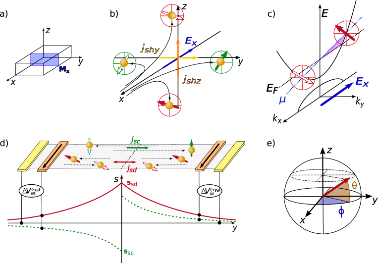
Resolving SHE and ISGE in nonlocal devices. Nonlocal spin-dependent measurements have been widely used to investigate CSI phenomena (valenzuela2006direct, ) and extract the polarization of the generated spins. There, a charge current is applied along the CSI region and the nonlocal voltage is measured between a FM detector and a reference outer metallic contact as a function of the orientation and magnitude of an applied magnetic field (valenzuela2006direct, ; WST2017, ; yan2017, ). When the spins originating from the SHE and the ISGE are perpendicular to each other, they can be fully resolved by investigating spin precession with in-plane and perpendicular magnetic fields (benitez2020tunable, ) or by means of a symmetry analysis under oblique magnetic fields (ghiasi2019charge, ; cavill2020proposal, ). These approaches are not sufficient in graphene-WTe2 or graphene-MoTe2 heterostructures, where the TMDC is conducting and has low-symmetry (zhao2020unconventional, ; zhao2020observation, ; safeer2019large, ). However, in such systems the spin density induced by the ISGE has no preferential direction, whereas the SHE induces a directed spin current. Therefore, it is possible to discern between the SHE and ISGE generated spins by simultaneously measuring the spin accumulation along the spin-current direction at opposite sides of the CSI region, as illustrated in Fig. 1d.
When the current is applied along in the CSI region (not shown in the Fig. 1d), the SHE creates spin currents along () and () (Fig. 1b), which coexist with the spin density induced by the ISGE (Fig. 1c). A direct comparison between at , , differentiates the spins associated to the spin current from those associated to the ISGE and (Fig. 1d). Indeed, the spin current component diffusing away from the CSI region, which originates from , generates opposite spin accumulation at , while the spin current , associated to the ISGE and , generates equal spin accumulation at . Therefore, whereas . Such measurements do not distinguish between the ISGE and , since both induce a spin density whose orientation does not vary in the CSI region (safeer2019room, ). Nevertheless, these components can in principle be disentangled by analysing as a function of the SOC-material thickness (sinova2015spin, ). In particular, when the thickness is much smaller than the spin relaxation length along , vanishes zhang2001prl ; stamm2017prl , and only ISGE contributes to the nonlocal signal.
With the previous considerations, we focus on fully characterizing the spins generated by and by means of spin precession using spin detectors located at . The steady-state spin diffusion and precession in the spin channel are governed by the Bloch diffusion equation torrey ; js1988 ; zutic2004 :
| (1) |
where and is the spin electrochemical potential for spins along , is electron gyromagnetic ratio, is the diffusion constant, and characterizes the spin lifetime . In the most general case, the injected spins have an arbitrary spin orientation. The CSI spin injection efficiency into the spin channel can be quantified using effective spin-polarization factors , with the corresponding spin currents with contributions from and , and the width of the channel. Assuming isotropic spin transport in the channel and that the FM detector is characterized by a magnetization along the direction and by a polarization efficiency , the nonlocal resistance for along and takes the respective general forms:
| (2) | |||
| (3) |
where and is the channel sheet resistance.
Fitting the spin precession response to Eqs. (2) and (3) determines . The spin-injection angles for spins moving towards , defined as and , fully characterize the orientation of the injected spins on both sides of the CSI region (Fig. 1e). Therefore, comparing with and with provides direct information on and . In addition, focusing on and , rather than , eliminates systematic errors deriving from potential differences in the FM detector polarizations.
CSI in graphene-WTe2. WTe2 is a layered TMDC, which is stable in the orthorhombic Td(Pmn21) phase. It is characterized by a lack of bulk inversion symmetry (Fig. 2a-b), a glide mirror plane , an out-of-plane two-fold screw rotational symmetry and a mirror plane perpendicular to the crystallographic direction (Fig. 2b). Multilayer Td-WTe2 is a type-II Weyl semimetal (soluyanov2015type, ; li2017evidence, ) while in monolayer form it is a 2D topological insulator (fei2017edge, ; tang2017quantum, ; wu2018observation, ). Considering the mirror crystal symmetries, in the SHE, while, in the ISGE, along can induce a spin density with spins oriented along and viceversa, but no spin density parallel to .
The graphene-WTe2 device fabrication follows the protocols established with other TMDCs (benitez2020tunable, ) (see Supplementary Information SI ). The WTe2 crystals were grown by chemical vapor transport, using bromine as a transport agent (dimitrov2020chemical, ). Their electronic and crystalline structure was investigated by x-ray photoelectron spectroscopy, angle-resolved photoemission spectroscopy, and Raman spectroscopy, all of them demonstrating high quality and confirming the Td phase (SI, ). The crystallographic orientation of the WTe2 crystal in the actual device (Fig. 2c) is obtained by means of linearly polarized Raman spectroscopy. Figure 3d shows the Raman spectra when the laser polarization is rotated an angle relative to the long-axis of the WTe2 flake (Fig. 2c). The intensity of the Raman modes A (164 cm-1) and A (212 cm-1) are known to change as a function of crystal orientation. As the ratio A/A is maximum at (Fig. 2e) then, in our device, (song2016scirep, ).
As the spin transport in graphene is isotropic Raes2016 , the parameters and (as well as ) in Eq (2) and (3) are extracted by measuring spin precession with out-of-plane in the two reference graphene devices at both sides of WTe2. The CSI is then investigated by applying a charge current along the WTe2 crystal ( direction). All measurements are carried out at room temperature.
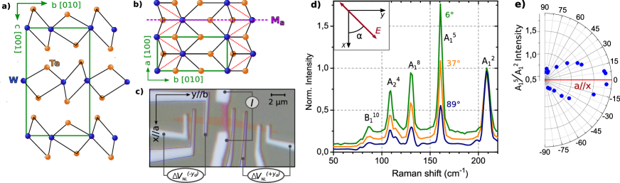
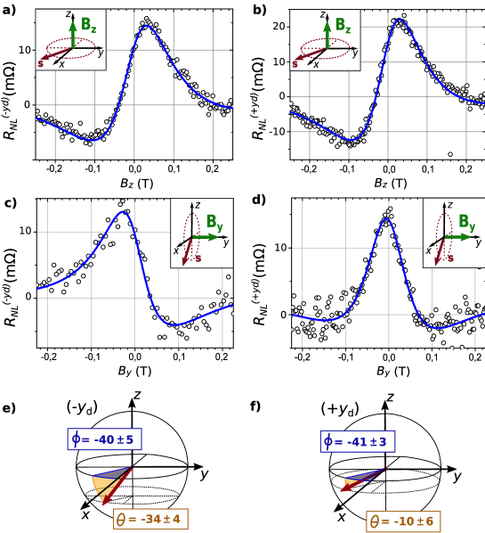
Figure 3 shows the nonlocal resistances and as a function of and . The signals have been acquired with the FM magnetizations saturated along both the directions to remove contributions that are unrelated to spin and associated to the magnetization rotation of the FM detector (SI, ). Remarkably, and present nearly undistinguishable lineshapes for (Figs. 3a and 3b), while this is clearly not the case for (Figs. 3c and 3d).
For , only the in-plane () components of the injected spins contribute to the precession lineshape. Therefore, the fact that demonstrates that the spins difussing towards and have the same in-plane spin polarization, which is an indication of a uniform in-plane polarization in the CSI region (associated to in Fig. 1d). Moreover, because are neither fully symmetric nor fully antisymmetric about , the spin polarization has nonzero components along both and .
In contrast, for only the spin components in the plane contribute to the precession lineshape. The marked difference between and demonstrates that the spins difussing towards and have different spin polarization orientation in the plane. Combined with the results for , this observation is an unambiguous indication of a spin polarized current in the CSI region with a polarization along (associated to in Fig. 1d). Furthermore, being rather symmetric about (Fig. 3d) also demonstrates the presence of a uniform spin density along , originating from , which partially compensates the contribution from .
To quantify the relative magnitudes of each CSI component, we fit the measurements in Fig. 3 to Eqs. (2) or (3). The fittings are shown with blue lines, from which the spin-polarization angles and are extracted: and (see Fig. 3e and 3f for a schematic representation). The spins originating from and relate to and , respectively. The presence of non-zero symmetric and antisymmetric angular components confirms the coexistence in the CSI region of spin-Hall currents along with polarization in and uniform spin densities with polarizations components on , and .
Origin of the observed CSI in graphene-WTe2. Although our experiments establish the presence of CSI with different symmetries, unequivocally identifying the underlying CSI mechanisms requires further analysis. The CSI can originate from either the ISGE or the SHE, in the bulk of WTe2, at the graphene-WTe2 interface or in graphene by proximity effects (JFS2021NatNano, ).
The spin density in the CSI region has components in all three directions (Fig. 3). According to the Td-WTe2 crystal symmetries, for a current in () only the spin-polarization component along () is allowed: the ISGE can generate a spin density in , while the spin Hall current flowing in should also be polarized along xue2020staggered . Therefore, the and components are not expected in the bulk of Td-WTe2, which indicates that both originate from interfacial or proximity-induced effects in graphene considering the reduced symmetry of the heterostructure xue2020staggered .
The symmetry of an heterostructure or thin crystal can be equal or lower than its bulk constituents, permitting additional non-zero spin polarization components. Indeed, in the graphene-WTe2 interface, the glide symmetry is absent, leaving possibly only the single mirror symmetry plane . As discussed in Fig. 1, the generation of a spin density in (), when is along (), would then be allowed.
The spin density along was previously observed in graphene-MoTe2 and graphene-WTe2 and was ascribed to the presence of an additional bulk mirror symmetry breaking induced by strain in the TMDC (safeer2019large, ; zhao2020unconventional, ). In our experiments, Raman spectroscopy demonstrates that WTe2 is not under strain (SI, ), making this explanation implausible. Alternatively, the spin density in could be generated by a current component along . Recent theoretical works reported anisotropic SHE in WTe2 and MoTe2 as a function of charge current direction and Fermi energy position zhou2019intrinsic ; vila2021low . However, the elongated geometry of our WTe2 flake (Fig. 2d) implies that the current component along is very small and a very large CSI efficiency would be required to make this scenario viable. These observations confirm that the spin density along is likely generated in the proximitized graphene.
Recent first-principles calculations addressing the twist-angle dependence of proximity-induced SOC in graphene by TMDCs MoS2, MoSe2, WS2 and WSe2 have shown that the Rashba SOC could exhibit a radial component, thus deviating from the typical tangential orientation naimer2021 . As discussed in refs. li2019twist ; naimer2021 , the radial component is allowed for twist angles between the graphene and TMDC lattices different from 0∘ and 30∘, where mirror symmetries are broken and the point group symmetry of graphene-TMDC is reduced to . Similarly, an arbitrary twist angle between the graphene and WTe2 crystal lattices can break the remaining symmetry upon reflection in . At their interface, with radial Rashba SOC coupling, a spin polarization component parallel to can then arise.
It remains to be understood why the radial component has never been observed in graphene-WS2 and graphene-MoS2 ghiasi2019charge ; safeer2019room ; benitez2020tunable . The high annealing temperatures used in those works, to clean the heterostructures and improve the interface quality, might have favored 0∘ or 30∘ twist angles, although this argument would not be valid if the initial (arbitrary) twist angle was larger than a few degrees. Therefore, further studies are required to address this question.
Finally, the observed spin current along , which is polarized in , has not been reported in prior graphene-WTe2 studies (zhao2020unconventional, ; zhao2020observation, ). It is however allowed even in high-symmetry structures, and has been reported in graphene-MoS2 and graphene-WS2 ghiasi2019charge ; safeer2019room ; benitez2020tunable . In these experiments, the generation of a spin density with polarization in was also found. It was further confirmed that both the spin current polarized in and the spin density in can originate solely from the SHE and the ISGE in proximitized graphene, respectively ghiasi2019charge ; benitez2020tunable . But, in general, the former could be due to the SHE, in graphene or in the TMDC, while the latter to the ISGE in graphene or the SHE in the TMDC safeer2019room .
The previous discussion strongly suggests that the unconventional CSI components in graphene-WTe2 originate from interfacial or proximity effects. In contrast, the observed spin current with polarization in and the spin densities in are permitted both in the bulk of Td-WTe2 and in proximitized graphene. Quantifying the spin absorption in WTe2 could in principle help separate these remaining CSI contributions, however, the analysis is not straightforward or free of ambiguities. The estimation of the spin absorption requires detailed knowledge of heterostructure properties that cannot be readily obtained in nonlocal devices. The properties include the precise interface resistance between graphene and WTe2 as well as the spin relaxation parameters in both the proximitized graphene and WTe2. Any subtle change in these parameters, or in the implementation of the spin absorption model, can result in diverging conclusions. In addition, due to the 2D nature of graphene, the spin absorption is not uniform at the graphene-WTe2 interface, even if the spin-current absorption occurs in direction. This can be easily understood by considering the inverse SHE, commonly used in CSI experiments. Because of spin relaxation and the fact that there is no alternative path for spins to cross the CSI region, as in a 3D system, the majority of spins will be absorbed on the side of graphene-WTe2 that is closest to the FM injector. This leads to a spin accumulation gradient (and a spin current) in the TMDC along the spin channel.
III CONCLUSIONS
We have demonstrated experimentally that the CSI in graphene-WTe2, with a current along the WTe2 axis, induces spin-polarized carriers with polarization components in all three spatial directions. By implementing systematic multi-terminal nonlocal spin precession experiments, we have shown that it is possible to disentangle the CSI from the spin Hall and inverse spin galvanic effects. A spin current flowing along the graphene channel leads to opposite spin polarization on the two sides of the CSI region, inducing a signal with opposite sign in remote FM detectors at each side. In contrast, a spin density in the CSI region produces a signal with equal sign in the same detectors.
We confirmed a spin accumulation with polarization along the applied current, which by symmetry is not allowed in the WTe2 bulk. Our analysis indicates that this spin accumulation originates at the graphene-WTe2 interface and involves the emergence of a radial component in the proximity-induced Rashba SOC, which arises from twisting li2019twist ; naimer2021 . To validate this interpretation, additional experiments are needed. In particular, the predicted radial component was predicted to be extremely sensitive to the twist angle, unintended doping and carrier density naimer2021 . Therefore, it is necessary to systematically address the dependence of the spin accumulation parallel to the current as a function of crystalline orientation, sample annealing temperature and gate voltage. For the latter, thin, ideally monolayer, WTe2 should be used to avoid both gate shielding (from semi-metallic bulk WTe2) and artifacts from spin absorption. Nevertheless, to unambiguously demonstrate the radial Rashba component, it might be better to simply focus on semiconducting TMDCs.
We also show, for the first time, the presence of spin currents and spin densities with polarization perpendicular to the substrate plane in graphene-WTe2. The observed spin polarization, as generated by the SHE spin current is always allowed, and can be induced in the bulk of WTe2 or in proximitized graphene. However, symmetry considerations show that the spin density with perpendicular polarization must originate from the ISGE at the graphene-WTe2 interface.
Overall, our work demonstrates that multi-terminal CSI measurements combined with symmetry analysis is a powerful approach to discriminate CSI signals. This is important for both applied and fundamental reasons. In particular, understanding the CSI originating from SHE and ISGE with all possible orientations is a promising route for magnetic memory applications, where the generation of unconventional spin-orbit torques is required macneil2017nphys .
IV ACKNOWLEDGEMENTS
We acknowledge support of the European Union’s Horizon 2020 FET-PROACTIVE project TOCHA under grant agreement 824140 and of the Spanish Research Agency (AEI), Ministry of Science and Innovation, under contracts no. PID2019-111773RB-I00/AEI/10.13039/501100011033, and SEV-2017-0706 Severo Ochoa. J. F. S acknowledges support from AEIunder contract RYC2019-028368-I/AEI/10.13039/50110001103, W. S. T from the European Union Horizon 2020 research and innovation program, grant number 881603 (Graphene Flagship), and I. F. A. of a fellowship from ”la Caixa” Foundation (ID 100010434) with code LCF/BQ/DI18/11660030 and of H2020 Marie Skłodowska-Curie grant agreement No. 713673.
References
- [1] RJ Elliott. Spin-orbit coupling in band theory—character tables for some” double” space groups. Physical Review, 96(2):280, 1954.
- [2] M Zahid Hasan and Charles L Kane. Colloquium: topological insulators. Reviews of modern physics, 82(4):3045, 2010.
- [3] AN Bogdanov and UK Rößler. Chiral symmetry breaking in magnetic thin films and multilayers. Physical review letters, 87(3):037203, 2001.
- [4] Charles L Kane and Eugene J Mele. Z 2 topological order and the quantum spin hall effect. Physical review letters, 95(14):146802, 2005.
- [5] Cui-Zu Chang and Mingda Li. Quantum anomalous hall effect in time-reversal-symmetry breaking topological insulators. Journal of Physics: Condensed Matter, 28(12):123002, 2016.
- [6] Aurelien Manchon, Hyun Cheol Koo, Junsaku Nitta, SM Frolov, and RA Duine. New perspectives for rashba spin–orbit coupling. Nature materials, 14(9):871–882, 2015.
- [7] Jairo Sinova, Sergio O Valenzuela, Jörg Wunderlich, CH Back, and T Jungwirth. Spin hall effects. Reviews of Modern Physics, 87(4):1213, 2015.
- [8] Anjan Soumyanarayanan, Nicolas Reyren, Albert Fert, and Christos Panagopoulos. Emergent phenomena induced by spin–orbit coupling at surfaces and interfaces. Nature, 539(7630):509–517, 2016.
- [9] R Galceran et al. Control of spin–charge conversion in van der waals heterostructures. APL Materials, 9:100901, 2021.
- [10] Mikhail I D’Yakonov and VI Perel. Possibility of orienting electron spins with current. Soviet Journal of Experimental and Theoretical Physics Letters, 13:467, 1971.
- [11] Mikhail I Dyakonov and VI Perel. Current-induced spin orientation of electrons in semiconductors. Physics Letters A, 35(6):459–460, 1971.
- [12] JE Hirsch. Spin hall effect. Physical review letters, 83(9):1834, 1999.
- [13] SD Ganichev, EL Ivchenko, VV Bel’Kov, SA Tarasenko, M Sollinger, Dieter Weiss, Werner Wegscheider, and Wilhelm Prettl. Spin-galvanic effect. Nature, 417(6885):153–156, 2002.
- [14] Lars Onsager. Reciprocal relations in irreversible processes. i. Physical Review, 37(4):405, 1931.
- [15] Philippe Jacquod, Robert S Whitney, Jonathan Meair, and Markus Büttiker. Onsager relations in coupled electric, thermoelectric, and spin transport: The tenfold way. Physical Review B, 86(15):155118, 2012.
- [16] Michael Victor Berry. Quantal phase factors accompanying adiabatic changes. Proceedings of the Royal Society of London. A. Mathematical and Physical Sciences, 392(1802):45–57, 1984.
- [17] Di Xiao, Ming-Che Chang, and Qian Niu. Berry phase effects on electronic properties. Reviews of modern physics, 82(3):1959, 2010.
- [18] Victor M Edelstein. Spin polarization of conduction electrons induced by electric current in two-dimensional asymmetric electron systems. Solid State Communications, 73(3):233–235, 1990.
- [19] Jun-Wei Luo, Gabriel Bester, and Alex Zunger. Full-zone spin splitting for electrons and holes in bulk gaas and gasb. Physical review letters, 102(5):056405, 2009.
- [20] Xiuwen Zhang, Qihang Liu, Jun-Wei Luo, Arthur J Freeman, and Alex Zunger. Hidden spin polarization in inversion-symmetric bulk crystals. Nature Physics, 10(5):387–393, 2014.
- [21] Yuichiro K Kato, Roberto C Myers, Arthur C Gossard, and David D Awschalom. Observation of the spin hall effect in semiconductors. Science, 306(5703):1910–1913, 2004.
- [22] Joerg Wunderlich, Bernd Kaestner, Jairo Sinova, and Tomas Jungwirth. Experimental observation of the spin-hall effect in a two-dimensional spin-orbit coupled semiconductor system. Physical Review Letters, 94(4):047204, 2005.
- [23] Sergio O Valenzuela and M Tinkham. Direct electronic measurement of the spin hall effect. Nature, 442(7099):176–179, 2006.
- [24] E Saitoh, M Ueda, H Miyajima, and G Tatara. Conversion of spin current into charge current at room temperature: Inverse spin-hall effect. Applied physics letters, 88(18):182509, 2006.
- [25] T Kimura, Y Otani, T Sato, S Takahashi, and S Maekawa. Room-temperature reversible spin hall effect. Physical review letters, 98(15):156601, 2007.
- [26] B Dieny et al. Opportunities and challenges for spintronics in the microelectronics industry. Nature Electronics, 3:446–459, 2020.
- [27] JF Sierra, J Fabian, RK Kawakami, S Roche, and SO Valenzuela. Van der waals heterostructures for spintronics and opto-spintronics. Nature Nanotechnology, 16:856–868, 2021.
- [28] Talieh S Ghiasi, Alexey A Kaverzin, Patrick J Blah, and Bart J van Wees. Charge-to-spin conversion by the rashba–edelstein effect in two-dimensional van der waals heterostructures up to room temperature. Nano letters, 19(9):5959–5966, 2019.
- [29] CK Safeer, Josep Ingla-Aynés, Franz Herling, José H Garcia, Marc Vila, Nerea Ontoso, M Reyes Calvo, Stephan Roche, Luis E Hueso, and Fèlix Casanova. Room-temperature spin hall effect in graphene/mos2 van der waals heterostructures. Nano letters, 19(2):1074–1082, 2019.
- [30] L Antonio Benitez, Williams Savero Torres, Juan F Sierra, Matias Timmermans, Jose H Garcia, Stephan Roche, Marius V Costache, and Sergio O Valenzuela. Tunable room-temperature spin galvanic and spin hall effects in van der waals heterostructures. Nature materials, 19(2):170–175, 2020.
- [31] JH Garcia, AW Cummings, and S Roche. Spin hall effect and weak antilocalization in graphene/transition metal dichalcogenide heterostructures. Nano letters, 17:5078–5083, 2017.
- [32] M Offidani, M Milletarì, R Raimondi, and A Ferreira. Optimal charge-to-spin conversion in graphene on transition-metal dichalcogenides. Physical Review Letters, 119:196801, 2017.
- [33] Stuart A Cavill, Chunli Huang, Manuel Offidani, Yu-Hsuan Lin, Miguel A Cazalilla, and Aires Ferreira. Proposal for unambiguous electrical detection of spin-charge conversion in lateral spin valves. Physical Review Letters, 124(23):236803, 2020.
- [34] CK Safeer, Nerea Ontoso, Josep Ingla-Aynés, Franz Herling, Van Tuong Pham, Annika Kurzmann, Klaus Ensslin, Andrey Chuvilin, Iñigo Robredo, Maia G Vergniory, et al. Large multidirectional spin-to-charge conversion in low-symmetry semimetal mote2 at room temperature. Nano letters, 19(12):8758–8766, 2019.
- [35] N Li and M Koshino. Twist-angle dependence of the proximity spin-orbit coupling in graphene on transition-metal dichalcogenides. Physical Review B, 99(2):075438, 2019.
- [36] Bing Zhao, Bogdan Karpiak, Dmitrii Khokhriakov, Annika Johansson, Anamul Md Hoque, Xiaoguang Xu, Yong Jiang, Ingrid Mertig, and Saroj P Dash. Unconventional charge–spin conversion in weyl-semimetal wte2. Advanced Materials, 32(38):2000818, 2020.
- [37] T Naimer et al. Twist-angle dependent proximity induced spin-orbit coupling in graphene/transition metal dichalcogenide heterostructures. Physical Review B, 104(2):195156, 2021.
- [38] D MacNeill et al. Control of spin–orbit torques through crystal symmetry in wte2/ferromagnet bilayers. Nature Physics, 13:300–305, 2017.
- [39] CK Safeer et al. Reliability of spin-to-charge conversion measurements in graphene-based lateral spin valves. 2D Materials, 9:015024, 2022.
- [40] Marten Seemann, Diemo Ködderitzsch, Sebastian Wimmer, and Hubert Ebert. Symmetry-imposed shape of linear response tensors. Physical Review B, 92(15):155138, 2015.
- [41] A Roy, M. H. D. Guimarães, and J Sławińska. Unconventional spin hall effects in nonmagnetic solids. Physical Review Materials, 6:045004, 2022.
- [42] Yu A Bychkov and Emmanuel I Rashba. Oscillatory effects and the magnetic susceptibility of carriers in inversion layers. Journal of physics C: Solid state physics, 17(33):6039, 1984.
- [43] Gustav Bihlmayer, O Rader, and Roland Winkler. Focus on the rashba effect. New journal of physics, 17(5):050202, 2015.
- [44] W Savero Torres et al. Spin precession and spin hall effect in monolayer graphene/pt nanostructures. 2D Materials, 4:041008, 2017.
- [45] W Yan et al. Large room temperature spin-to-charge conversion signals in a few-layer graphene/pt lateral heterostructure. Nature Communications, 8:661, 2017.
- [46] Bing Zhao, Dmitrii Khokhriakov, Yang Zhang, Huixia Fu, Bogdan Karpiak, Anamul Md Hoque, Xiaoguang Xu, Yong Jiang, Binghai Yan, and Saroj P Dash. Observation of charge to spin conversion in weyl semimetal wte 2 at room temperature. Physical Review Research, 2(1):013286, 2020.
- [47] S Zhang. Spin hall effect in the presence ofspin diffusion. Physical Review Letters, 85:393, 2001.
- [48] C Stamm et al. Magneto-optical detection of the spin hall effect in pt and w thin films. Physical Review Letters, 119:087203, 2017.
- [49] H. C. Torrey. Bloch equations with diffusion terms. Physical Review, 104:563, 1956.
- [50] M Johnson and R. H. Silsbee. Coupling of electronic charge and spin at a ferromagnetic-paramagnetic metal interface. Physical Review B, 37:5312, 1988.
- [51] Igor Z̆utić, Jaroslav Fabian, and S. Das Sarma. Spintronics: Fundamentals and applications. Reviews of Modern Physics, 76:323, 2004.
- [52] Alexey A Soluyanov, Dominik Gresch, Zhijun Wang, QuanSheng Wu, Matthias Troyer, Xi Dai, and B Andrei Bernevig. Type-ii weyl semimetals. Nature, 527(7579):495–498, 2015.
- [53] Peng Li, Yan Wen, Xin He, Qiang Zhang, Chuan Xia, Zhi-Ming Yu, Shengyuan A Yang, Zhiyong Zhu, Husam N Alshareef, and Xi-Xiang Zhang. Evidence for topological type-ii weyl semimetal wte 2. Nature communications, 8(1):1–8, 2017.
- [54] Zaiyao Fei, Tauno Palomaki, Sanfeng Wu, Wenjin Zhao, Xinghan Cai, Bosong Sun, Paul Nguyen, Joseph Finney, Xiaodong Xu, and David H Cobden. Edge conduction in monolayer wte 2. Nature Physics, 13(7):677–682, 2017.
- [55] Shujie Tang, Chaofan Zhang, Dillon Wong, Zahra Pedramrazi, Hsin-Zon Tsai, Chunjing Jia, Brian Moritz, Martin Claassen, Hyejin Ryu, Salman Kahn, et al. Quantum spin hall state in monolayer 1t’-wte 2. Nature Physics, 13(7):683–687, 2017.
- [56] Sanfeng Wu, Valla Fatemi, Quinn D Gibson, Kenji Watanabe, Takashi Taniguchi, Robert J Cava, and Pablo Jarillo-Herrero. Observation of the quantum spin hall effect up to 100 kelvin in a monolayer crystal. Science, 359(6371):76–79, 2018.
- [57] . Supplementary information. ., .
- [58] Krastyo Buchkov, Rosen Todorov, Penka Terziyska, Marin Gospodinov, Velichka Strijkova, Dimitre Dimitrov, and Vera Marinova. Anisotropic optical response of wte2 single crystals studied by ellipsometric analysis. Nanomaterials, 11(9):2262, 2021.
- [59] Q Song et al. The in-plane anisotropy of wte2 investigated by angle-dependent and polarized raman spectroscopy. Scientific Reports, 6(8):29254, 2016.
- [60] B Raes et al. Determination of the spin-lifetime anisotropy in graphene using oblique spin precession. Nature Communications, 7:11444, 2016.
- [61] F Xue and PM Haney. Staggered spin hall conductivity. Physical Review B, 102(2):195146, 2020.
- [62] Jiaqi Zhou, Junfeng Qiao, Arnaud Bournel, and Weisheng Zhao. Intrinsic spin hall conductivity of the semimetals mote 2 and wte 2. Physical Review B, 99(6):060408, 2019.
- [63] M Vila et al. Low-symmetry topological materials for large charge-to-spin interconversion: The case of transition metal dichalcogenide monolayers. Physical Review Reseach, 3:043230, 2021.