Modular nanomagnet design for spin qubits confined in a linear chain
Abstract
On-chip micromagnets enable electrically controlled quantum gates on electron spin qubits. Extending the concept to a large number of qubits is challenging in terms of providing large enough driving gradients and individual addressability. Here we present a design aimed at driving spin qubits arranged in a linear chain and strongly confined in directions lateral to the chain. Nanomagnets are placed laterally to one side of the qubit chain, one nanomagnet per two qubits. The individual magnets are ”U”-shaped, such that the magnetic shape anisotropy orients the magnetization alternately towards and against the qubit chain even if an external magnetic field is applied along the qubit chain. The longitudinal and transversal stray field components serve as addressability and driving fields. Using micromagnetic simulations we calculate driving and dephasing rates and the corresponding qubit quality factor. The concept is validated with spin-polarized scanning electron microscopy of Fe nanomagnets fabricated on silicon substrates, finding excellent agreement with micromagnetic simulations. Several features required for a scalable spin qubit design are met in our approach: strong driving and weak dephasing gradients, reduced crosstalk and operation at low external magnetic field.
Single-qubit gates in electron-spin qubits are typically implemented with electron dipole spin resonance (EDSR) enabled by a magnetic field gradient Watson et al. (2018); Kawakami et al. (2014); Takeda et al. (2016); Pioro-Ladrière et al. (2008). Successful operation of up to 6 qubits with a common micromagnet has been demonstrated Philips et al. (2022). Despite its current success, scaling this technique to drive and address thousands of single qubits remains challenging Gonzalez-Zalba et al. (2021); Tadokoro et al. (2021); Boter et al. (2022); Nakamura et al. (2022); Yoneda et al. (2015) because the magnetic stray field needs to fulfill different requirements at the same time. It should provide: (i) large driving gradients to achieve a fast Rabi frequency , (ii) a difference in Larmor frequencies between neighboring qubits significantly larger than for qubit addressability with low crosstalk and (iii) small gradients of its longitudinal field component to prevent spin dephasing.
A possible strategy to address this challenge is to place individual nanomagnets close to the quantum dots that define the qubits, e.g. by co-integration of the magnets with the hosting structure. For this purpose, platforms offering an inherent confinement into a one-dimensional geometry such as Si nanowires Froning et al. (2018) or finFETs Kuhlmann et al. (2018) are of advantage, since less conventional gate electrodes are needed to control the qubits, freeing up space to place the nanomagnets. In the finFET platform, electron spin qubits have been realized by a CMOS fab-compatible process Zwerver et al. (2022). Due to the strong lateral confinement induced by the fin, the displacement of the electron wavefunction for EDSR driving is preferably induced along the fin, i.e. along the qubit chain. This is different compared to currently established micromagnet designs, where a displacement transverse to the qubit chain is used to drive EDSR Yoneda et al. (2015); Philips et al. (2022); Zwerver et al. (2022).
In this letter we present a modular design of nanomagnets aimed at driving a large number of spin qubits arranged in a linear chain and strongly confined in directions lateral to the chain. We have simulated and fabricated ”U”-shaped Fe nanomagnets down to a feature size of nm. Their magnetization pattern has been imaged by spin-polarized scanning electron microscopy (spin-SEM) Allenspach (2000), showing excellent agreement with micromagnetic simulations. We discuss sweet spots for reduced influence of charge noise and reduced crosstalk in EDSR driving and investigate how these properties depend on the alignment accuracy between nanomagnets and the spin qubits. The concept presented provides a scalable approach to EDSR driving of electron spins and can be implemented in several spin qubit platforms ranging from FinFETs to nanowires and planar geometries.
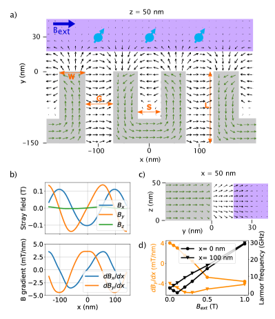
Figs. 1(a) and (c) show top and side views of our design. Individual ”U”-shaped nanomagnets are placed laterally to one side of the qubit chain, one nanomagnet per two qubits. The two ends of the ”U” point towards the qubit chain. Because of magnetic shape anisotropy, the magnetization in the two arms of each nanomagnet points in an alternating way towards and against the chain even with an external magnetic field applied along the qubit chain. This creates a gradient in the stray field component transverse to the external field. This gradient is used to drive Rabi oscillations of the spin qubits by spatially oscillating the position of the host electron in the direction along the chain. The sign of the longitudinal component of the stray field alternates from qubit to qubit, which together with provides large differences in the Larmor frequencies of neighboring qubits and enables addressability with low crosstalk.
Micromagnetic simulations have been performed with the software package MuMax3 Vansteenkiste et al. (2014). We choose Fe as the magnetic material and assume a saturation magnetization of 1.7 MA/m, an exchange stiffness of 21 pJ/m, a cell size of 1 nm and zero temperature. The plane defines the sample surface, with the qubit chain oriented along the direction. The nanomagnets have an arm width nm, length nm, thickness nm, separation nm between the arms and nm between the magnets, which results in a qubit-qubit pitch of nm. Smaller pitches can be implemented by decreasing the size of and , which would further increase the attainable driving gradient at the qubit locations.
The stray field of the nanomagnet at T is represented in a quiver plot in Fig. 1(a) and (d). Its longitudinal ( component) maxima and minima coincide with the zero-crossings of its transverse () component [Fig. 1(b)], setting optimal locations for the qubits at the center of the nanomagnets nm (”arm”) and in between them at nm (”gap”). At nm and nm, the driving gradient reaches 3.9 mT/nm at the ”arm” position and -4.8 mT/nm at the ”center” position, see also Table 1. Together with a zero-crossing of the dephasing gradient , these positions define a sweet spot.
The electric field that induces the oscillatory spatial displacement of the electron wavefunction of an individual quantum dot will unavoidably also affect neighboring qubits. Individual addressability therefore requires qubit frequencies to be separated far enough to only resonantly excite one qubit, which translates into having distinct magnetic fields among neighboring qubits. At neighboring qubit positions, has opposite signs, and together with a finite , of these qubits will be different. We find that at T, GHz (”arm”) and GHz (”gap”), assuming an electron g-factor of [Fig. 1(d)]. When set to 0.10 T, matches such that at the ”arm” location. For T, the driving gradient decreases significantly due to the reorientation of the magnetization pattern in the arms. At T, the magnetization almost saturates everywhere into the direction and neighbouring qubits approach the same Larmor frequency. The magnitude of the driving gradient then approaches the values at low fields.
Hence, in our design has to be adjusted such that its magnitude is as low as possible to preserve a high driving gradient and at the same time high enough to allow for single qubit addressability. These values for can be significantly smaller than what is commonly used in EDSR experiments and simulations with micromagnets Watson et al. (2018); Kawakami et al. (2014); Takeda et al. (2016); Pioro-Ladrière et al. (2008); Philips et al. (2022); Struck et al. (2020); Yoneda et al. (2018); Neumann and Schreiber (2015); Chesi et al. (2014).
Several advantages arise at low values of . Firstly, a lower leads to reduced crosstalk between neighboring drive lines, due to the frequency dependence of their capacitive coupling Teske et al. (2022). Secondly, less demanding control electronics is required. Thirdly, the spin relaxation time is increased Glavin and Kim (2003), also avoiding hot spots when the Zeeman energy coincides with the valley splitting Huang and Hu (2014). Finally, coherent shuttling of qubits is facilitated at low fields, since the acquired spin phase during shuttling is directly dependent on the magnitude of Langrock et al. (2022).
The design summarized in Fig. 1 has four main advantages with respect to previous micromagnet designs: enhanced addressability between neighboring qubits at low external field (difference in is above 2.5 GHz at T), stronger driving gradient ( mT/nm), a zero-crossing in the dephasing gradient and a modular design that can be extended to arbitrarily long chains of spin qubits.
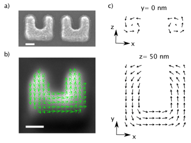
We have fabricated such ”U”-shaped nanomagnets on a silicon substrate covered by native oxide, using e-beam lithography on a PMMA-based bilayer followed by e-beam evaporation and lift-off of 50 nm of Fe and 3 nm of Pd as a capping layer. Before the magnetic measurements, the capping layer was removed in ultrahigh vacuum by Ne ion sputtering. An in-plane magnetic field pulse of 17 mT was applied along to orient the bases of the magnets along the same direction. The magnets were then investigated in remanence (i.e. at ) by spin-SEM, where topography and magnetization distribution of the first 2 nm of the sample surface are simultaneously determined with a lateral resolution of approximately 10 nm.
In Fig. 2(a) we show an SEM image of the fabricated nanomagnets. The patterning process caused the edges to be rounded with respect to the geometry used in the simulations. This rounding is also visible in the spin-SEM image in Fig. 2(b), where an arrow-plot combining both in-plane magnetization components is overlaid on top of the topographic data. The magnetization follows the shape of the magnet similar to that obtained in the simulations at T shown in Fig. 2(c). Deviations between simulation and experimental magnetization pattern are found in the rounded region at the apices of the arms. In Fig. 2(b) we see that the magnetization rotates its direction at the apex of both arms along the direction. This is compatible with the vortex visible in the simulation cut at nm in Fig. 2(c).
We investigate the impact of the vortex formation by comparing the simulation described in Fig. 1 (”relaxed”) with a hypothetical nanomagnet with arms uniformly magnetized in opposite directions (”uniform”). We see that the rearrangement of the magnetization pattern reduces the driving gradient as well as at both qubit positions (Table 1).
A smaller stray field is also found in the simulation where nanomagnets have a rounded apex (”rounded’). We approximate the shape of the nanomagnet apex [Fig. 2(a)] with a semi-cylinder with a diameter of nm. All other simulation parameters are identical to the ”relaxed” case. The comparison between these two geometries shows a reduction of the driving gradients by at both qubit locations for the ”rounded” case. This reduction is ascribed to the smaller amount of magnetic material present in the vicinity of the qubit.
| Position | uniform | relaxed | rounded | |
|---|---|---|---|---|
| gap | (mT/nm) | |||
| (GHz) | ||||
| arm | (mT/nm) | |||
| (GHz) | ||||
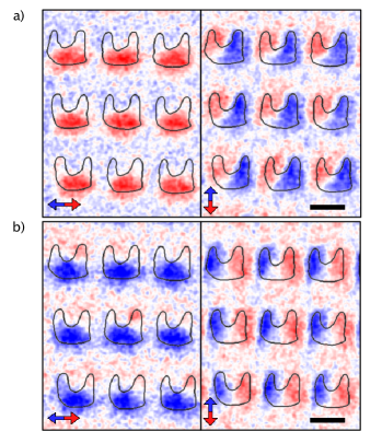
Scalabe designs of one-dimensional arrays of qubits can be implemented by repeating the nanomagnets along the chain, provided that magnetization patterns among the different nanomagnets are similar. In Fig. 3 we show both in-plane magnetization components of a 3 by 3 nanomagnet array after applying a magnetic pulse of 17 mT along and . We extract the nanomagnets contour from the topographic data and overlay it on the magnetic measurement images. The comparison of the magnetization components between the two measurements demonstrates a symmetrical reversal of the magnetization pattern for opposite magnetic field directions, with the bases of the magnets oriented along the direction of the magnetic pulse and the arms alternating between and . Upon closer inspection, we see in the horizontal magnetization images that the magnetization at the apices is partially oriented along the direction, as already noted in Fig. 2(b). The sign of this component varies among the different apices, suggesting a varying chirality of the vortices, both within and between structures. We believe that the chirality is induced by random local defects, and according to the micromagnetic simulations, the energy difference between nanomagnets with identical or opposite vortex chirality is negligible. The vortex chirality has no significant impact on the driving gradient or addressability at the foreseen qubit positions.
Large driving gradients are accompanied by large dephasing gradients and may limit the fidelity of qubit operations. We therefore calculate the dephasing time and quality factor that we expect from the ”U”-shaped nanomagnets. Charge noise has been identified as the main limitation to the gate fidelity of single-qubit gates for micromagnet-based EDSR Struck et al. (2020); Yoneda et al. (2018), and will be considered as the dephasing mechanism in the following. We assume that the charge noise has a 1/f power spectrum Yoneda et al. (2018); Nakajima et al. (2020); Dumoulin Stuyck et al. (2021). The noise in electric field will translate into noise in the spatial position of the electron wavefunction and through the dephasing gradient into noise in . The relevant dephasing gradients are , and , since the and stray field components are negligible at the qubit position [Fig. 1(b)]. The gradients are calculated in a 50 x 50 nm2 area by fitting the simulated stray field with a quadratic polynomial at each mesh point and taking the first derivative of the fitted polynomial. Higher orders lead to significantly smaller contributions and are neglected in the following.
The dephasing rate for each direction is calculated by assuming root-mean-square displacements along the direction Nakajima et al. (2020) with :
| (1) |
where is the electron gyromagnetic ratio (g-factor of 2), Planck’s constant and the approximated first derivative of the stray field along the direction. We assume pm Kawakami et al. (2014) and pm. The larger is justified by the weaker confinement of the quantum dot along that direction. The dephasing time is then .
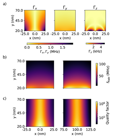
Fig. 4(a) shows the calculated dephasing rates , and as a function of the qubit position around the ”arm” position. At nm, is zero, and the same is true for the position ”gap” at nm (data not shown). provides the main source of dephasing, whereas is negligible within the simulated range. We note that because the magnetic field is rotation-free outside the nanomagnets , and therefore the maxima in the driving field at the ”arm” and ”gap” positions coincide with maxima in . Here, the strong confinement of the electron wavefunction in the fin reduces displacements along the direction, thus mitigating dephasing.
We calculate the quality factor , an upper bound for the qubit fidelity Takeda et al. (2016). The Rabi dephasing time is Nakajima et al. (2020), and the Rabi frequency is
| (2) |
The factor defines a power noise spectrum of the qubit frequency. We obtain from the relation Nakajima et al. (2020) , where () is the highest (lowest) frequency of noise the qubit is exposed to, and is the root-mean-square of the qubit frequency noise. The latter is obtained from calculated above by the relation . We assume MHz and Hz, similar to the experiment in Ref. Struck et al. (2020), and a displacement amplitude of 500 pm from the EDSR drive, similar to Teske et al. (2022). Fig. 4(b) shows the expected Rabi frequency, highlighting an increase in value with decreasing distance between the qubit and the nanomagnet, similar to the stray field trend visible in Fig. 1(a).
The quality factor is smoothed by a Gaussian filter with a sigma-width of 5 nm, compatible with a full-width at half maximum of the dot size in plane of 12 nm [Fig. 4(c)]. We see that the qubits are optimally placed at positions aligned with the center of the magnet and the gap between them, corresponding to the dephasing minimum positions described before. The weak dependency of on the -coordinate is due to the equality between the driving gradient and the main dephasing gradient (), as a consequence of Ampère’s law. On the other hand, we see a strong dependence on the alignment of the qubit, caused by corresponding increase of . Misalignment of 3 nm in the direction reduces the quality factor by 30 %. Nevertheless, quality factors higher than are achieved within 15 nm of misplacement, which exceeds the alignment precision of standard e-beam lithography Raith (2015). Note that the quoted values for depend on the assumed displacement noise and scale inversely with and therefore also inversely with the square of the dephasing gradient.
In conclusion, we have shown a nanomagnet design aimed at driving a linear chain of qubits that are strongly confined in directions lateral to the chain. EDSR can be performed with an external magnetic field below the saturation field of the nanomagnets, which is advantageous for operation of spin qubits at lower frequencies. At the foreseen locations, neighboring qubits differ in Larmor frequency by more than GHz. We found reproducible magnetization of fabricated nanomagnets and excellent agreement with micromagnetic simulations. The qubits are expected to have have quality factors greater than with alignment tolerances relative to the nanomagnet positions that are within reach for e-beam lithography. The modularity of the design opens up the possibility to address a large number of qubits aligned along a linear chain.
Acknowledgements.
We thank the Cleanroom Operations Team of the Binnig and Rohrer Nanotechnology Center (BRNC), Matthias Mergenthaler, Nico Hendrickx, Felix Schupp for advise on sample processing, Andreas Fuhrer, Patrick Harvey-Collard and Andrea Ruffino for discussions, Eoin Kelly for proof-reading the manuscript and Andreas Bischof and Stephan Paredes for support in the lab. This work was supported as a part of NCCR SPIN funded by the Swiss National Science Foundation (grant number 51NF40-180604).References
- Watson et al. (2018) T. F. Watson, S. G. Philips, E. Kawakami, D. R. Ward, P. Scarlino, M. Veldhorst, D. E. Savage, M. G. Lagally, M. Friesen, S. N. Coppersmith, M. A. Eriksson, and L. M. Vandersypen, Nature 555, 633 (2018).
- Kawakami et al. (2014) E. Kawakami, P. Scarlino, D. R. Ward, F. R. Braakman, D. E. Savage, M. G. Lagally, M. Friesen, S. N. Coppersmith, M. A. Eriksson, and L. M. Vandersypen, Nature Nanotechnology 9, 666 (2014).
- Takeda et al. (2016) K. Takeda, J. Kamioka, T. Otsuka, J. Yoneda, T. Nakajima, M. R. Delbecq, S. Amaha, G. Allison, T. Kodera, S. Oda, et al., Science Advances 2, e1600694 (2016).
- Pioro-Ladrière et al. (2008) M. Pioro-Ladrière, T. Obata, Y. Tokura, Y. S. Shin, T. Kubo, K. Yoshida, T. Taniyama, and S. Tarucha, Nature Physics 4, 776 (2008).
- Philips et al. (2022) S. G. Philips, M. T. Madzik, S. V. Amitonov, S. L. de Snoo, M. Russ, N. Kalhor, C. Volk, W. I. Lawrie, D. Brousse, L. Tryputen, B. P. Wuetz, A. Sammak, M. Veldhorst, G. Scappucci, and L. M. Vandersypen, Nature 4, 919 (2022).
- Gonzalez-Zalba et al. (2021) M. Gonzalez-Zalba, S. de Franceschi, E. Charbon, T. Meunier, M. Vinet, and A. Dzurak, Nature Electronics 4, 872 (2021).
- Tadokoro et al. (2021) M. Tadokoro, T. Nakajima, T. Kobayashi, K. Takeda, A. Noiri, K. Tomari, J. Yoneda, S. Tarucha, and T. Kodera, Scientific Reports 11, 19406 (2021).
- Boter et al. (2022) J. M. Boter, J. P. Dehollain, J. P. van Dijk, Y. Xu, T. Hensgens, R. Versluis, H. W. Naus, J. S. Clarke, M. Veldhorst, F. Sebastiano, and L. M. Vandersypen, Phys. Rev. Appl. 18, 024053 (2022).
- Nakamura et al. (2022) S. Nakamura, H. Kiyama, and A. Oiwa, Journal of Applied Physics 132, 224301 (2022).
- Yoneda et al. (2015) J. Yoneda, T. Otsuka, T. Takakura, M. Pioro-Ladrière, R. Brunner, H. Lu, T. Nakajima, T. Obata, A. Noiri, C. J. Palmstrøm, et al., Applied Physics Express 8, 084401 (2015).
- Froning et al. (2018) F. N. M. Froning, M. K. Rehmann, J. Ridderbos, M. Brauns, F. A. Zwanenburg, A. Li, E. P. A. M. Bakkers, D. M. Zumbühl, and F. R. Braakman, Applied Physics Letters 113, 073102 (2018), https://doi.org/10.1063/1.5042501 .
- Kuhlmann et al. (2018) A. V. Kuhlmann, V. Deshpande, L. C. Camenzind, D. M. Zumbühl, and A. Fuhrer, Applied Physics Letters 113, 122107 (2018).
- Zwerver et al. (2022) A. Zwerver, T. Krähenmann, T. Watson, L. Lampert, H. C. George, R. Pillarisetty, S. Bojarski, P. Amin, S. Amitonov, J. Boter, et al., Nature Electronics 5, 184 (2022).
- Allenspach (2000) R. Allenspach, IBM Journal of Research and Development 44, 553 (2000).
- Vansteenkiste et al. (2014) A. Vansteenkiste, J. Leliaert, M. Dvornik, M. Helsen, F. Garcia-Sanchez, and B. Van Waeyenberge, AIP Advances 4, 107133 (2014).
- Struck et al. (2020) T. Struck, A. Hollmann, F. Schauer, O. Fedorets, A. Schmidbauer, K. Sawano, H. Riemann, N. V. Abrosimov, Ł. Cywiński, D. Bougeard, et al., npj Quantum Information 6, 1 (2020).
- Yoneda et al. (2018) J. Yoneda, K. Takeda, T. Otsuka, T. Nakajima, M. R. Delbecq, G. Allison, T. Honda, T. Kodera, S. Oda, Y. Hoshi, et al., Nature Nanotechnology 13, 102 (2018).
- Neumann and Schreiber (2015) R. Neumann and L. Schreiber, Journal of Applied Physics 117, 193903 (2015).
- Chesi et al. (2014) S. Chesi, Y.-D. Wang, J. Yoneda, T. Otsuka, S. Tarucha, and D. Loss, Physical Review B 90, 235311 (2014).
- Teske et al. (2022) J. D. Teske, F. Butt, P. Cerfontaine, G. Burkard, and H. Bluhm, arXiv preprint arXiv:2208.10548 (2022).
- Glavin and Kim (2003) B. Glavin and K. Kim, Physical Review B 68, 045308 (2003).
- Huang and Hu (2014) P. Huang and X. Hu, Physical Review B 90, 235315 (2014).
- Langrock et al. (2022) V. Langrock, J. A. Krzywda, N. Focke, I. Seidler, L. R. Schreiber, and Ł. Cywiński, arXiv preprint arXiv:2202.11793 (2022).
- Nakajima et al. (2020) T. Nakajima, A. Noiri, K. Kawasaki, J. Yoneda, P. Stano, S. Amaha, T. Otsuka, K. Takeda, M. R. Delbecq, G. Allison, et al., Physical Review X 10, 011060 (2020).
- Dumoulin Stuyck et al. (2021) N. I. Dumoulin Stuyck, F. A. Mohiyaddin, R. Li, M. Heyns, B. Govoreanu, and I. P. Radu, Applied Physics Letters 119, 094001 (2021), https://doi.org/10.1063/5.0059939 .
- Raith (2015) Raith, “Datasheet ebpg5200 plus,” https://raith.com/product/ebpg-plus/ (2015), accessed: 2022-12-01.