Impact of different metal electrodes on the ferroelectric properties of hafnium-zirconium oxide in M1/FE/M2 structures during the electric field cycling
Abstract
The interest in the ferroelectric non-volatile memory as a candidate for low power consumption electronic memories was raised after the discovery of ferroelectricity in hafnium oxide. Doping by different elements of hafnia films allows improving their ferroelectric properties. In this work, the transport experiments are combined with the simulations to study the evolution of ferroelectric properties and the mean distance between oxygen vacancies during the endurance of hafnium-zirconium oxide in metal-ferroelectric-metal structures to study the impact of different metal electrodes.
pacs:
72.20.Jv, 77.55.df, 77.84.Bw, 73.50.h, 72.80.r, 85.50.GkThe development of memory devices for using them in mobile systems, Internet-of-Things technology and in other devices with high autonomy requires non-volatile energy efficiency and high operation speed from used memory elements. One of the candidates for the role of such memory is Ferroelectric Random Access Memory (FRAM). The modern FRAM research is centered around the study of the ferroelectric properties of doped thin \ceHfO2 films, since FRAM devices based on lead zirconate-titanate (\cePZT) [1] are not scalable beyond the nm CMOS technology. This limitation is due to a dramatic decrease in the ferroelectric properties of a \cePZT film with a reduction in its thickness less than nm. The history of ferroelectric \ceHfO2 began in , when the group members at the Dynamic Random Access Memory (DRAM) company Qimonda, together with the RWTH Aachen, searched for materials for DRAM capacitor applications and unexpectedly discovered the ferroelectric properties of doped thin \ceHfO2 films. It was demonstrated that the non-centrosymmetric polar orthorhombic phase (o-phase) between the monoclinic (m-) and tetragonal (t-) phase grains in thin (– nm) doped \ceHfO2 layers is responsible for maintaining polarization after the external electric field is turned off [2, 3, 4]. The \ceHfO2-based FRAM technology demonstrates non-volatility, high information volume per die, high operation speed and is compatible with the modern CMOS technology [5].
For more than years, researchers were working to solve problems that prevent the implementation of \ceHfO2-based FRAM devices into mass-market production. The main problems include a small memory window, a small memory cell resource and instability of the memory window during its operation. A small memory window (double value of the remnant polarization (MW) prevents a reliable reading logical state of the memory cell. A small memory cell resource (endurance) is little information rewriting cycles before the memory cell fails (breakdown). The MW instability during the operation (cycling) consists in an increase in MW at the beginning of cycling (wake-up effect) and a decrease in the memory window before a breakdown (fatigue effect) [6, 7]. These problems can be solved by selecting doping \ceHfO2 material followed by rapid thermal annealing at high temperatures. It was found that, the largest memory window is reached when using \ceLa as a dopant [8]. Also, when using \ceHf_0.5Zr_0.5O2 instead of \ceHfO2, the wake-up effect is suppressed and the annealing temperature decreases [9], which is compatible with the thermal budget of back-end-of-line. The ferroelectric response of the structure is also influenced by the method of metal contacts deposition and the annealing temperature. The highest memory window value for \ceHf_0.5Zr_0.5O2 films without doping was obtained by applying the in vacuo process, without atmospheric influence on the structure, which made it possible to obtain a memory window of µC/cm2 due to the improvement of the ferroelectric/metal interface quality [10]. Recently, it has been discovered that when \ceHf_0.5Zr_0.5O2 is doped with \ceLa, \ceY and their mixture, the films remain functional after rewriting cycles, demonstrating quite a large MW value [11, 12]. However, doping with \ceLa led to a more pronounced manifestation of the wake-up effect.
The possible reason of this effect might be caused by the influence of metal electrodes. The \ceHf_0.5Zr_0.5O2:\ceLa-based structures in Refs. 11, 12 had both bottom (BE) and top (TE) \ceTiN metal electrodes. Recently, it has been shown that using \ceRuO2 as the TE in \ceTiN/\ceHf_0.5Zr_0.5O2/\ceRuO2 [13], as both the TE and the BE in \ceRuO2/\ceHf_0.5Zr_0.5O2/\ceRuO2 [14] and \ceRu as the BE in \ceRu/\ceHf_0.5Zr_0.5O2/\ceTiN [15] structures leads to a small memory window value and a relatively early breakdown during the electric field cycling. Other metal electrodes were explored to promote the ferroelectric phase in \ceHf_1-xZr_xO2 including \ceTaN [16, 17], \ceIr [18, 19], \cePt [20, 21, 22] and \ceW [23] without endurance measurements.
In this letter, we investigate the impact of different metal electrodes of \ceHf_0.5Zr_0.5O2 in metal-ferroelectric-metal structures during the endurance cycling.
| Sample | Structure | BE | TE |
|---|---|---|---|
| S1 | \ceTiN/\ceHf_0.5Zr_0.5O2/\ceTiN | \ceTiN | \ceTiN |
| S2 | \ceTiN/\ceHf_0.5Zr_0.5O2/\ceRuO_x | \ceTiN | \ceRuO_x |
| S3 | \ceTiN/\ceHf_0.5Zr_0.5O2/\ceTiAlN | \ceTiN | \ceTiAlN |
| S4 | \ceTiN/\ceHf_0.5Zr_0.5O2/\ceNbN | \ceTiN | \ceNbN |
| S5 | \ceW/\ceHf_0.5Zr_0.5O2/\ceTiN | \ceW | \ceTiN |
| S6 | \ceW/\ceHf_0.5Zr_0.5O2/\ceW | \ceW | \ceW |
| S7 | \ceTiN/\ceHf_0.5Zr_0.5O2/\ceW | \ceTiN | \ceW |
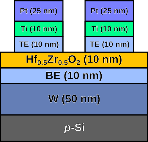
The structures under study in this work were metal-1/\ceHf_0.5Zr_0.5O2/metal-2 (M1/FE/M2) ferroelectric capacitors on silicon substrates with the ferroelectric thicknesses of nm. Totally, seven kinds of samples with different electrodes were studied. A description of all samples is provided in Table 1. M1/FE/M2 capacitors were fabricated by the following procedure. The nm thick \ceW layer, as well as nm thick TE and BE were deposited on a silicon substrate at room temperature using a sputtering system from Alliance Concept. To produce S5 and S6 samples, the BE deposition step was skipped, i.e. \ceHf_0.5Zr_0.5O2 films for these structures were deposited directly on the \ceW layers. The nm thick \ceHf_0.5Zr_0.5O2 films were deposited by atomic layer deposition (ALD) at deposition temperature \celsius in the Oxford Instruments OPAL system. For hafnium and zirconium oxides, tetrakis[ethylmethylamino]hafnium (\ceHf[N(C2H5)CH3]4) and tris(dimethylamino)cyclopentadienyl-zirconium (\ceC5H5)Zr[N(CH3)2]3) were used as precursors, respectively. \ceH2O was used as an oxidant for all ALD cycles. The samples were then treated by RTA at \celsius for min in the \ceN2 atmosphere. To pattern the capacitor structures, a nm thick \ceTi layer was deposited as an adhesion layer, and then nm thick \cePt was deposited by the electron beam evaporation through a shadow mask. The round-shaped metal contact diameter was µm. The wet chemical etching of TE was carried out for patterning using the SC1 etching ( \ceNH3 and \ceH2O2 solutions in \ceH2O at the temperature of \celsius). The schematic structures of the samples under study with different BE and TE are shown in Fig. 1. To produce S2, S6 and S7 samples, the \ceTiN electrode top was removed by SC1 etching, and then \ceRuO2 or \ceW electrodes were deposited by physical vapor deposition through a shadow mask on the \ceHf_0.5Zr_0.5O2 films.
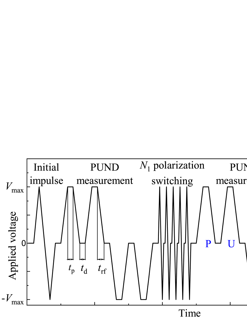
An experimental study of the ferroelectric properties evolution during the structure state switching was carried out by the cyclic application of trapezoidal voltage pulses of positive and negative amplitudes. On some pulses, polarization-voltage (-) characteristics were measured by the PUND technique followed by the DC current-voltage (-) measurements with the same voltage amplitude. The measurements by the PUND method consist in the sequential application of two positive pulses (Positive/Up) and two negative (Negative/Down) to the structure. The PUND sequences and cyclic voltage pulses are shown in Fig. 2 schematically. The remnant polarization values during the cycling were obtained from the PUND measurements. For the PUND measurements, the voltage rise/fall times , pulse delay and plateau time were the same and amounted µs. The times for the cycling pulses were µs, µs and µs. The cycling pulse durations ensure that the polarization is switched to at least of the maximum possible value. The voltage of all pulses was V̇, since at this amplitude value a compromise ratio of the memory window and the cycling duration was observed (see supplementary Fig. S1). The DC measurements were carried out from to V in V increments for sec. Such long voltage sweep duration allows us to reduce the displacement current contributions and to extract their values at zero voltage. The measurements were carried out using a Keithley 4200-SCS parametric analyzer with 4225-PMU (pulses and PUND) and SMU-4210 (DC) units at room temperature. The experiments were carried out up to the sample break down or when becomes negligible.
Following the PUND method, DC measurements made it possible to obtain leakage currents. As a result of averaging the currents measured during the forward () and reverse () voltage sweep, displacement currents were excluded, and leakage currents were obtained:
| (1) |
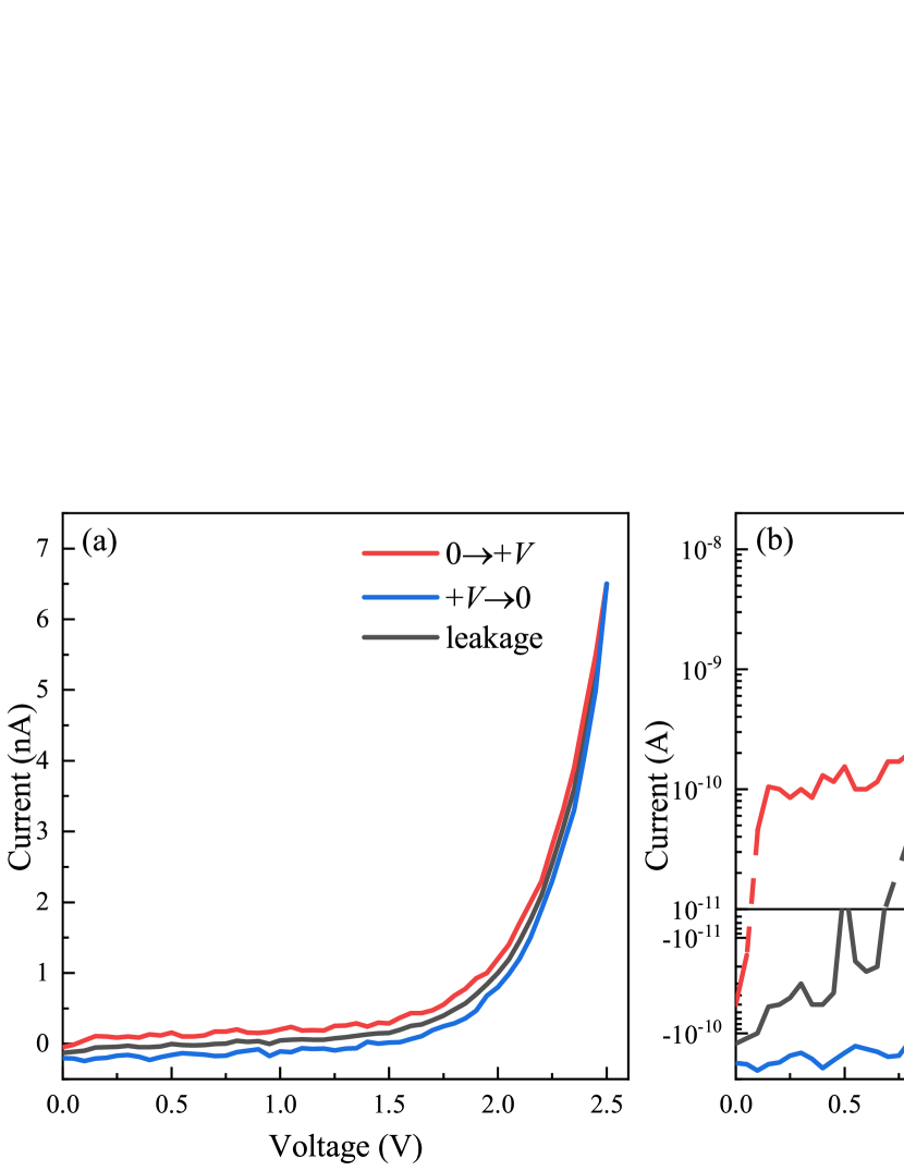
The procedure for extracting the leakage current is illustrated in Fig. 3. The mean distance between neighboring traps was extracted from the - dependences of the leakage currents within the model of phonon-assisted tunneling of electrons (holes) between neighboring traps (PATENT) [24]. Recently, it has been demonstrated that this transport model adequately describes the leakages in both amorphous and ferroelectric \ceHfO2-based films [25, 26, 27] as well as in \ceHf_0.5Zr_0.5O2-based structures [28, 29, 30]. This procedure is described in details elsewhere [30, 27, 31].
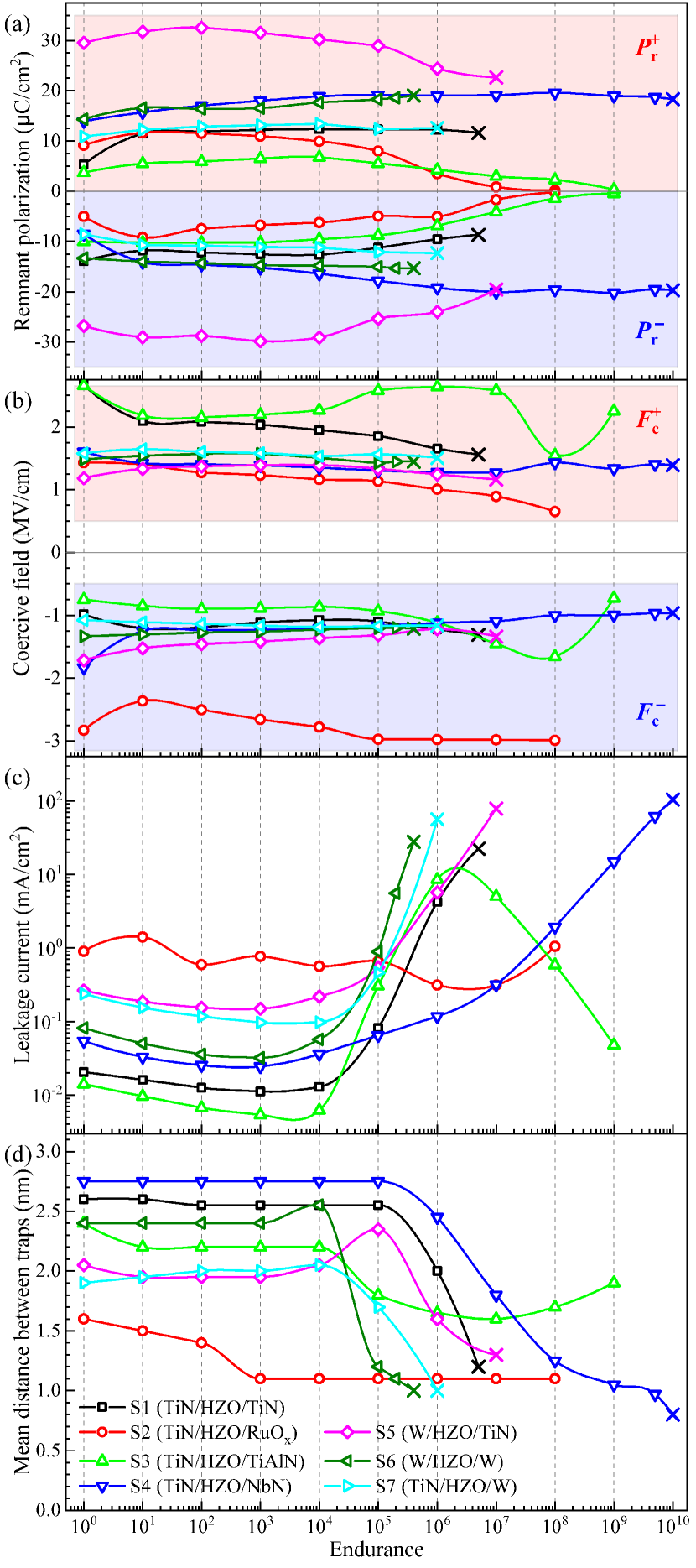
The presence of \ceHf_0.5Zr_0.5O2 film ferroelectric properties is confirmed by observing the hysteresis in the polarization-voltage characteristics for all M1/FE/M2 structures (See supplementary Fig. S2–S4). In Fig. 4 is the evolution of the ferroelectric and transport properties of M1/FE/M2 structures with different bottom and top metal electrodes. The S1 sample with \ceTiN BE and TE exhibits a typical MW () evolution (black characters in Fig. 4) in accordance with literature data [32, 30]: it endures more than switch cycles with a slight wake-up and fatigue effects with µC/cm2 and then breaks down, as shown in Fig. 4 by crosses. The MW () values for S2 and S3 samples are less than µC/cm2 and disappear after – switching cycles. The S5 sample exhibits the largest remnant polarization with µC/cm2 and a long fatigue and breaks down after endurance cycles. The MW values for samples S1, S4, S6 and S7 are close, but all of them, except S4, are broken down after – switch cycles. The sample with \ceNbN TE (S4) endures more than repolarization with – µC/cm2.
The coercive field values (Fig. 4) are constant with small deviations for almost all structures under study except for S2 and S3 samples. As far as the MW disappears, loses its physical meaning. One can see that measured values exhibit slight asymmetry. This can be caused by built-in electric field due to different work functions of the metal electrodes. Also, asymmetric interfaces around ferroelectric films, due to the exposure of all BEs to the ALD processing temperature, can introduce distortions in the measurements.
The leakage currents, measured at the voltage of V are shown in Fig. 4. One can see that leakages rise after cycles for all structures, but the S2 sample, which exhibits constant leakage current. The leakage current of structure S3 shows complex evolution: namely, it increases after endurance cycles, but dramatically decreases after cycles.
The extracted mean distances between neighboring traps are shown in Fig. 4. One can see that the distance between traps does not change until the leakage currents start to rise exponentially. As soon as the distance between traps decrease, the leakages increases due to their exponential dependence.
Since the traps in \ceHf_0.5Zr_0.5O2 are oxygen vacancies, a decrease in the distances between traps is associated with new oxygen vacancy generation [28, 30]. Oxygen ions that left the crystal lattice can migrate in an external electric field and even leave the \ceHf_0.5Zr_0.5O2 film for a metal electrode [33]. The S4 structure is formed with the top \ceNbN electrode, i.e., it is more corrosion and oxidation resistant than \ceTiN [34]. Thus, the \ceTiN electrode in the structures absorbs more oxygen than \ceNbN. This effect leads to a greater endurance of the structure during repolarization even with a large number of defects. It is difficult to determine where new oxygen vacancies are located. We assume that, initially, there are many traps (oxygen vacancies) in the grain boundaries and much less in the grain bulk. Thus, the leakage current is caused by traps at the grain boundaries, and there is a voltage drop between the bulk \ceHf_0.5Zr_0.5O2 and the electrode due to the interface (e.g. \ceTiON for \ceTiN) [35]. After cycles new traps are generated in the grain bulk due to the oxygen ion migration during the cyclic switching, and some ions might reach grain boundaries or even the \ceHf_0.5Zr_0.5O2/metal interface followed by the absorption of electrodes. Then the leakage currents are limited by the traps in the grain bulk. If the traps are located in the grain boundaries, then the mean distance between the traps can be converted to the surface (2D) trap density – cm-2. If the traps are distributed in the grain bulk, then the volumetric (3D) trap density is – cm-3.
It is interesting to note that the S5 structure with \ceW BE exhibits an extremely high MW value, compared to other structures. We assume that this is caused by the absence of the interface sub-layer (IL) after the \ceHf_0.5Zr_0.5O2 deposition. The endurance cycling leads to a fast generation of new oxygen vacancies in \ceHf_0.5Zr_0.5O2, forming the IL followed by a breakdown. \ceRuO_x and \ceTiAlN electrodes absorb oxygen more actively than other metals, the interface sublayer is formed faster, and the voltage drops on the IL [36]. This leads to the vanishing of the ferroelectric response in \ceHf_0.5Zr_0.5O2 films and decrease in leakage currents. It should be noted that these samples were not broken down. One can assume that \ceRuO_x and \ceTiAlN electrodes are good for the DRAM application.
Also, it is interesting to note that S5 and S7 structures are symmetrical to each other, but exhibit their different ferroelectric evolution during the endurance procedure. We assume that this is caused by different temperature regimes of the ferroelectric film synthesis on the BE (\celsius) and the TE on \ceHf_0.5Zr_0.5O2 (room temperature). It should be noted that not only the electrode material, but also its specific properties such as grain texture can affect the \ceHf_0.5Zr_0.5O2 film properties and performance. The study of the metal electrodes structural properties and their effect on the \ceHf_0.5Zr_0.5O2 film ferroelectric properties is beyond the scope of this work and is a task for the future.
In conclusion, transport experiments, combined with simulations, were studied for thin \ceHf_0.5Zr_0.5O2 ferroelectric film-based structures with different metal electrodes. It was found that \ceRuO_x and \ceTiAlN electrodes suppress the ferroelectric response in \ceHf_0.5Zr_0.5O2 films, as well as leakages through the structure. The utilization of \ceNbN as an electrode in M/FE/M structures allows obtaining a more stable ferroelectric capacitor with more than cycle switches.
Supplementary Material
See the supplementary material for the memory window evolution during endurance cycling with different amplitudes for the S1 samples with different top electrode size and polarization-voltage characteristics for all samples.
Acknowledgements.
This work was supported by the Russian Foundation for Basic Research, Grant No. 20-57-12003 NNIO_a, and under the state contract with ISP SB RAS, No. 0306-2019-0005 (Code FWGW-2022-0003). The authors would like to express their gratitude to Prof. Thomas Mikolajick, Dr. Uwe Schroeder, Ruben Alcala and Monica Materano for the provided samples. The authors would like to acknowledge and thank Dr. Uwe Schroeder and Dr. Alexey Mironov for their valuable discussions.Conflict of Interest
The authors have no conflicts to disclose.
Data Availability
The data that support the findings of this study are available from the corresponding author upon reasonable request.
References
- Bondurant [1990] D. Bondurant, Ferroelectrics 112, 273 (1990).
- Böscke et al. [2011a] T. S. Böscke, J. Müller, D. Bräuhaus, U. Schröder, and U. Böttger, Applied Physics Letters 99, 102903 (2011a).
- Böscke et al. [2011b] T. S. Böscke, S. Teichert, D. Bräuhaus, J. Müller, U. Schröder, U. Böttger, and T. Mikolajick, Applied Physics Letters 99, 112904 (2011b).
- Sang et al. [2015] X. Sang, E. D. Grimley, T. Schenk, U. Schroeder, and J. M. LeBeau, Applied Physics Letters 106, 162905 (2015).
- Trentzsch et al. [2016] M. Trentzsch, S. Flachowsky, R. Richter, J. Paul, B. Reimer, D. Utess, S. Jansen, H. Mulaosmanovic, S. Muller, S. Slesazeck, J. Ocker, M. Noack, J. Muller, P. Polakowski, J. Schreiter, S. Beyer, T. Mikolajick, and B. Rice, in 2016 IEEE International Electron Devices Meeting (IEDM) (IEEE, 2016) pp. 11.5.1–11.5.4.
- Mueller et al. [2013] S. Mueller, J. Muller, U. Schroeder, and T. Mikolajick, IEEE Trans. Device Mater. Rel. 13, 93 (2013).
- Pesič et al. [2016] M. Pesič, F. P. G. Fengler, S. Slesazeck, U. Schroeder, T. Mikolajick, L. Larcher, and A. Padovani, in 2016 IEEE International Reliability Physics Symposium (IRPS) (IEEE, 2016) pp. MY–3–1–MY–3–5.
- Schroeder et al. [2014] U. Schroeder, E. Yurchuk, J. Müller, D. Martin, T. Schenk, P. Polakowski, C. Adelmann, M. I. Popovici, S. V. Kalinin, and T. Mikolajick, Japanese Journal of Applied Physics 53, 08LE02 (2014).
- Kim et al. [2016] H. J. Kim, M. H. Park, Y. J. Kim, Y. H. Lee, T. Moon, K. D. Kim, S. D. Hyun, and C. S. Hwang, Nanoscale 8, 1383 (2016).
- Lee et al. [2021] Y. Lee, H. Alex Hsain, S. S. Fields, S. T. Jaszewski, M. D. Horgan, P. G. Edgington, J. F. Ihlefeld, G. N. Parsons, and J. L. Jones, Applied Physics Letters 118, 012903 (2021).
- Kozodaev et al. [2019] M. G. Kozodaev, A. G. Chernikova, E. V. Korostylev, M. H. Park, R. R. Khakimov, C. S. Hwang, and A. M. Markeev, Journal of Applied Physics 125, 034101 (2019).
- Popovici et al. [2022] M. I. Popovici, A. M. Walke, J. Bizindavyi, J. Meersschaut, K. Banerjee, G. Potoms, K. Katcko, G. Van den Bosch, R. Delhougne, G. S. Kar, and J. Van Houdt, ACS Applied Electronic Materials 4, 1823 (2022).
- Park et al. [2014a] M. H. Park, H. J. Kim, Y. J. Kim, W. Jeon, T. Moon, and C. S. Hwang, physica status solidi (RRL) — Rapid Research Letters 8, 532 (2014a).
- Fields et al. [2021] S. S. Fields, S. W. Smith, S. T. Jaszewski, T. Mimura, D. A. Dickie, G. Esteves, M. David Henry, S. L. Wolfley, P. S. Davids, and J. F. Ihlefeld, Journal of Applied Physics 130, 134101 (2021).
- Chernikova et al. [2020] A. G. Chernikova, M. G. Kozodaev, R. R. Khakimov, S. N. Polyakov, and A. M. Markeev, Applied Physics Letters 117, 192902 (2020).
- Migita et al. [2018] S. Migita, H. Ota, H. Yamada, K. Shibuya, A. Sawa, and A. Toriumi, Japanese Journal of Applied Physics 57, 04FB01 (2018).
- Smith et al. [2017] S. W. Smith, A. R. Kitahara, M. A. Rodriguez, M. D. Henry, M. T. Brumbach, and J. F. Ihlefeld, Applied Physics Letters 110, 072901 (2017).
- Park et al. [2014b] M. H. Park, H. J. Kim, Y. J. Kim, W. Lee, T. Moon, K. D. Kim, and C. S. Hwang, Applied Physics Letters 105, 072902 (2014b).
- Shimizu et al. [2014] T. Shimizu, T. Yokouchi, T. Shiraishi, T. Oikawa, P. S. S. R. Krishnan, and H. Funakubo, Japanese Journal of Applied Physics 53, 09PA04 (2014).
- Hyuk Park et al. [2013] M. Hyuk Park, H. Joon Kim, Y. Jin Kim, W. Lee, H. Kyeom Kim, and C. Seong Hwang, Applied Physics Letters 102, 112914 (2013).
- Park et al. [2014c] M. H. Park, H. J. Kim, Y. J. Kim, T. Moon, and C. S. Hwang, Applied Physics Letters 104, 072901 (2014c).
- Shimizu et al. [2015] T. Shimizu, T. Yokouchi, T. Oikawa, T. Shiraishi, T. Kiguchi, A. Akama, T. J. Konno, A. Gruverman, and H. Funakubo, Applied Physics Letters 106, 112904 (2015).
- Karbasian et al. [2017] G. Karbasian, R. dos Reis, A. K. Yadav, A. J. Tan, C. Hu, and S. Salahuddin, Applied Physics Letters 111, 022907 (2017).
- Nasyrov and Gritsenko [2011] K. A. Nasyrov and V. A. Gritsenko, Journal of Applied Physics 109, 093705 (2011).
- Islamov et al. [2014] D. R. Islamov, V. A. Gritsenko, C. H. Cheng, and A. Chin, Applied Physics Letters 105, 222901 (2014), arXiv:1409.6887 [cond-mat.mtrl-sci] .
- Gritsenko et al. [2016] V. A. Gritsenko, T. V. Perevalov, and D. R. Islamov, Physics Reports 613, 1 (2016).
- Gritsenko and Gismatulin [2020] V. A. Gritsenko and A. A. Gismatulin, Applied Physics Letters 117, 142901 (2020).
- Islamov et al. [2015a] D. R. Islamov, T. V. Perevalov, V. A. Gritsenko, C. H. Cheng, and A. Chin, Applied Physics Letters 106, 102906 (2015a), arXiv:1501.02370 [cond-mat.mtrl-sci] .
- Islamov et al. [2015b] D. R. Islamov, A. G. Chernikova, M. G. Kozodaev, A. M. Markeev, T. V. Perevalov, V. A. Gritsenko, and O. M. Orlov, JETP Letters 102, 544 (2015b).
- Islamov et al. [2019] D. R. Islamov, V. A. Gritsenko, T. V. Perevalov, V. A. Pustovarov, O. M. Orlov, A. G. Chernikova, A. M. Markeev, S. Slesazeck, U. Schroeder, T. Mikolajick, and G. Y. Krasnikov, Acta Materialia 166, 47 (2019).
- Pil’nik et al. [2020] A. A. Pil’nik, A. A. Chernov, and D. R. Islamov, Scientific Reports 10, 15759 (2020).
- Müller et al. [2011] J. Müller, T. S. Böscke, D. Bräuhaus, U. Schröder, U. Böttger, J. Sundqvist, P. Kücher, T. Mikolajick, and L. Frey, Applied Physics Letters 99, 112901 (2011).
- Nukala et al. [2021] P. Nukala, M. Ahmadi, Y. Wei, S. de Graaf, E. Stylianidis, T. Chakrabortty, S. Matzen, H. W. Zandbergen, A. Björling, D. Mannix, D. Carbone, B. Kooi, and B. Noheda, Science 372, 630 (2021).
- Barshilia et al. [2004] H. C. Barshilia, M. S. Prakash, A. Poojari, and K. S. Rajam, Thin Solid Films 460, 133 (2004).
- Grimley et al. [2016] E. D. Grimley, T. Schenk, X. Sang, M. Pešić, U. Schroeder, T. Mikolajick, and J. M. LeBeau, Advanced Electronic Materials 2, 1600173 (2016).
- Alcala et al. [2022] R. Alcala, F. Mehmood, P. Vishnumurthy, T. Mittmann, T. Mikolajick, and U. Schroeder, in 2022 IEEE International Memory Workshop (IMW) (IEEE, 2022).