Sophisticated deep learning with on-chip optical diffractive tensor processing
Abstract
The ever-growing deep learning technologies are making revolutionary changes for modern life. However, conventional computing architectures are designed to process sequential and digital programs, being extremely burdened with performing massive parallel and adaptive deep learning applications. Photonic integrated circuits provide an efficient approach to mitigate bandwidth limitations and power-wall brought by its electronic counterparts, showing great potential in ultrafast and energy-free high-performance computation. Here, we propose an optical computing architecture enabled by on-chip diffraction to implement convolutional acceleration, termed optical convolution unit (OCU). We demonstrate that any real-valued convolution kernels can be exploited by OCU with a prominent computational throughput boosting via the concept of structral re-parameterization. With OCU as the fundamental unit, we build an optical convolutional neural network (oCNN) to implement two popular deep learning tasks: classification and regression. For classification, Fashion-MNIST and CIFAR-4 datasets are tested with accuracy of 91.63% and 86.25%, respectively. For regression, we build an optical denoising convolutional neural network (oDnCNN) to handle Gaussian noise in gray scale images with noise level , resulting clean images with average PSNR of 31.70dB, 29.39dB and 27.72dB, respectively. The proposed OCU presents remarkable performance of low energy consumption and high information density due to its fully passive nature and compact footprint, providing a highly parallel while lightweight solution for future compute-in-memory architecture to handle high dimensional tensors in deep learning.
1 Introduction
Convolutional neural networks (CNNs) [1, 2, 3] powers enormous applications in artificial intelligence (AI) world including computer vision [4, 5, 6], self-driving cars [7, 8, 9] , natural language processing [10, 11, 12], medical science [13, 14, 15], etc. Inspired by biological behaviors of visual cortex systems, CNNs have brought remarkable breakthroughs in manipulating high-dimensional tensor such as images, videos and speech, enabling efficient processing with more precise information extractions but much fewer network parameters, compared with the classical feed-forward one. However, advanced CNN algorithms have rigorous requirements on computing platforms who are responsible for massive data throughputs and computations, which triggers a flourishing development of high performance computing hardware such as central processing unit (CPU) [16], graphics processing unit (GPU) [17], tensor processing unit (TPU) [18], and field-programmable gate array (FPGA) [19]. Nonetheless, today’s electronic computing architectures are facing physical bottlenecks in processing distribute and parallel tensor operations, mainly are bandwidth limitation, high-power consumption, and the fading of Moore’s Law, causing serious computation force mismatches between AI and the underlying hardware frameworks.
Important progresses have been made to further improve the capabilities of future computing hardware. In recent years, optical neural network (ONN) [20, 21, 22, 23, 24, 25, 26, 27] receives growing attentions with its extraordinary performances in facilitating complex neuromorphic computations. The intrinsic parallelism nature of optics enables more than 10-THz interconnection bandwidth[28], and the analog fashion of photonics system [29] decouplings the urgent needs for high-performance memory in conventional electronic architectures, and therefore prevents energy wasting and time latency from continuous AD/DA conversion and ALU-memory communication, boosting computational speed and reducing power consumption essentially.
To date, numerous ONNs are proposed to apply various neuromorphic computations such as optical inference networks based on MZI mesh[30, 31, 32], photonics spiking neural networks based on WDM protocol and ring modulator array [33, 34, 35], photonics tensor core based on phase change materials [36, 37], optical accelerator based on time-wavelength interleaving [38, 39, 40], etc. For higher computation capabilities of ONNs, diffractive optical neural networks [41, 42, 43, 44] are proposed to provide millions of trainable connections and neurons optically by means of light diffraction. In our previous work [45], we demonstrated an integrated diffractive optical neural network in SOI platform to further improve network density with metasurface technologies. Here, we make one step forward to build an optical convolution unit (OCU) with the same method to achieve massive parallel tensor computations. We demonstrate that any real-valued convolution kernels can be exploited by OCU with a prominent computation power. Furthermore, with OCU as the basic building block, we build an optical convolutional neural network (oCNN) to perform classification and regression tasks. For classification task, Fashion-MNIST and CIFAR-4 datasets are tested with accuracies of 91.63% and 86.25%, respectively. For regression task, we build an optical denoising convolutional neural network (oDnCNN) to handle Gaussian noise in gray scale images with noise level , resulting clean images with average PSNR of 31.70dB, 29.39dB and 27.72dB. The proposed OCU and oCNN are fully passive in processing massive tensor data and compatible for ultrahigh bandwidth interfaces (for both electronic and optical), being capable of integrating with electronic processors to re-aggregate computational resources and power penalty.
2 Principle
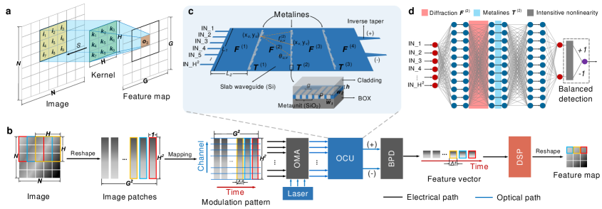
Fig.1(a) presents the operation principle of 2D convolution. Here, a fixed kernel K with size of slides over the image I with size of by stride of and does weighted addition with the image patches that cover by the kernel, resulting an extracted feature map O with size of , where (in this case we ignore the padding process of convolution). This process can be expressed in Eq.(1), where represents a pixel of the feature map, and are related to the stride . Based on this, one can simplify the operation as multiplications between a vector that reshaped by the kernel and a matrix that composed by image patches, as shown in Eq.(2).
| (1) |
| (2) |
Here, where denotes a corresponding image patch covered by a sliding kernel and is the flattened feature vector. Consequently, the fundamental idea of optical 2D convolution is to manipulate multiple vector-vector multiplications optically and keep their products in series for reshaping to a new map. Here, we use on-chip optical diffraction to implement this process, as described in Fig.1(b). The input image with size of is firstly reshaped into flattened patches according to the kernel size H and sliding stride S, which turns the image into a matrix . Then is mapped into a plane of space channels and time, in which each row of is varied temporarily with period of and each column of (namely pixels of a flattened image patch) are distributed in channels. A coherent laser signal is split into paths and then modulated individually by the time-encoded and channel-distributed image patches, in either amplitude or phase. In this way, one time slot with duration of contains one image patch with pixels in corresponding channels, and of these time slots can fully express image patch matrix . Then the coded light is sent to the proposed OCU to perform matrix multiplications as Eq.(2) shows, and the corresponding positive and negative results are detected by a balanced photodetector (BPD) to do subtractions between the two. The balanced detection scheme assures OCU operates in real-valued field. The detected information is varied temporarily with symbol duration of , and then reshaped into a new feature map by a digital signal processor (DSP).
The details of OCU are given in Fig.1(c). Here, silicon strip waveguides are exploited for receiving signals simultaneously from modulation channels, who diffract and interfere with each other in a silicon slab waveguide with size of before it encounters well-designed 1D-metalines. The 1D-metaline is a sub-wavelength grating consists of silica slots with each slot has size of , which is illustrated in the inset of Fig.1(c). Furthermore, we use 3 identical slots with slot gap of g to constitute a metaunit with period of to ensure a constant effective refractive index of the 1D-metaline when it meets light from different angles, as demonstrated in our previous work [45]. The incoming signal is phase-modulated from 0 to by changing the length of each metaunit but with and fixed. Accordingly, the corresponding length of the v-th metaunit in the l-th metaline can be ascertained from the introduced phase delay by Eq.(3), where and are the effective refractive index of the slab and slots respectively. After layers of propagation, the interfered light is sent to two ports which outputs positive and negative part of computing results.
| (3) |
| (4) |
For a more precise analysis, the diffraction in the slab waveguide between two metalines with U and V metaunits respectively is characterized by a matrix based on Huygens-Fresnel principle under restricted propagation conditions, whose element , as shown in Eq.(4), is the diffractive connection between the u-th metaunit locates at of the ()-th metaline and the v-th metaunit locates at in the l-th metaline, cos =, denotes the distance between the two metaunits, is working wavelength, j is imaginary unit, and are amplitude and phase coefficients, respectively. As for each metaline, the introduced phase modulations is modeled by a diagonal matrix , as expressed in Eq.(5):
| (5) |
To proof the accuracy of the proposed model in Eq.(4) and Eq.(5), we evaluate the optical field of an OCU with finite-different time-domain (FDTD) method as shown in Fig.2(a). Three metalines with 10 metaunits for each are configured based on a standard SOI platform, the size of slab waveguide between metalines is , the width and gap of slots are set to be 200nm and 500nm, the period of metaunit is 1.5um, and a laser source is split to 9 waveguides with working wavelength of 1550nm. We monitor the amplitude and phase response of the diffracted optical field in position A of Fig.2(a), who are well-agreed with the proposed analytical model in Eq.(4), as shown in Fig.2(b) and (c). Phase modulation of the metaline is also validated by monitoring the optical phase response at position B in Fig.2(d), with the incident light of a plane wave. Fig.2(e) shows a great match between the FDTD calculation and the analytical model in Eq.(5).
Consequently, we conclude the OCU model in Eq.(6), where M is the layer number of OCU and is the response of the OCU when the input is a reshaped image patch matrix . Besides, the numbers of metaunits in M metaline layers are all designed to be V, which leads to and (l = 1, 2, …, M-2) are matrices with size of . Specifically, is a matrix since the waveguides are exploited and is a matrix since we only focus on the signals at two output ports.
| (6) |
Therefore, is a matrix with column of and , which are vectors, and the corresponding response of balanced detection is described in Eq.(7) accordingly, where denotes a Hadamard product and is a amplitude coefficient introduced by the photodetection:
| (7) |
Furthermore, the OCU and balanced detection model in Eq.(6) and Eq.(7) can be abstracted as a feedforward neural network as illustrated in Fig.1(d), where the dense connections denotes diffractions and the single connections are phase modulations introduced by metalines. BPD’s square-law detection performs as a nonlinear activation in the network since the phase-involved computing makes the network complex-valued [46, 47, 48].
Note that it is rarely possible to build a one-to-one mapping between the metaunit lengths and kernel value directly, because the phase modulation of metalines introduce complex-valued computations while the kernels are usually real-valued. However, the feedforward linear neural network nature of OCU model facilitates another approach to implement 2D convolution optically. Structural re-parameterization [49, 50, 51] (SRP) is a networking algorithm in deep learning, in which the original network structure can be substituted equivalently with another one to obtain same outputs, as illustrated in Fig.3. Here, we leverage this concept to make a regression between the diffractive feedforward neural network and 2D convolution. In another word, we train the network to learn how to perform 2D convolution instead of mapping the kernel value directly into metaunit lengths. More details are shown in following sections.
3 Results
In this section, we evaluate the performance of OCU in different aspects of deep learning. In subsection A, we present the basic idea of 2D optical convolution with the concept of SRP, and we demonstrate that the proposed OCU is capable of representing arbitrary real-valued convolution kernel (in our following demos, we take ) and therefore implementing basic image convolution optically. In subsection B, we take the OCU as a fundamental unit to build an oCNN, with which classification and regression applications of deep learning are carried out with remarkable performances.
3.1 Optical convolution functioning
As mentioned above, an OCU can not be mapped from a real-valued kernel directly since the phase modulation of metalines makes the OCU model a complex-valued feedforward neural network. Therefore, we need to train the OCU to ”behave” as a real-valued convolution model with SRP method, which is referred as the training phase of OCU, and this idea is illustrated in Fig.4(a). We utilize a random pattern as the training set to make a convolution with a real-valued kernel, and the corresponding result is reshaped as a training label . Then we apply the training set on the OCU model to get a feature vector and calculate a mean square error (MSE) loss with the collected label. Through the iteration of backward propagation algorithm on our model, all the trainable parameters are updated to minimize loss and the OCU is evolved to the targeting real-valued kernel, as shown in Eq.(8) and Eq.(9), where is metaline-introduced phase and it is also the trainable parameter of OCU. Accordingly, images can be convolved with the well-trained OCU, and we term this process as an inference phase, as presented in Fig.4(b).
| (8) |
| (9) |
For proof-of-concept, a random pattern (the OCU’s performance gets almost no improvement with a random pattern that is larger than ) and 8 unique real-valued convolution kernels are exploited to generate training labels and a gray scale image is utilized to test the OCUs’ performance, as shown in Fig.5. In this case, we use 3 layers of metalines in OCU with = 75um and = 300um, each metaline consists of 50 metaunits with = 200nm, = 500nm and = 1.5um, the number of input waveguides are set to be 9 according to the size of the utilized real-valued kernel. The training and inference process of OCU are conducted with Tensorflow2.4.1 framework. From Fig.5 we can see great matches between the ground truths generated by real-valued kernels and the outputs generated by OCUs, and the average MSE between the two can be calculated as 0.0405, indicating that the OCU can response as a real-valued convolution kernel with remarkable performance.
3.2 Optical convolutional neural network (oCNN)
With OCU as the basic unit for feature extraction, more sophisticated architectures can be carried out efficiently to interpret the hidden mysteries in higher dimensional tensors. In this section, we build an optical convolutional neural network (oCNN) to implement tasks in two important topics of deep learning: classification and regression.
3.2.1 Image classification
Fig.6 shows the basic architecture of oCNN for image classifications. Images with size of are firstly flatten into groups of patches and concatenated as a data batch with size of according to the kernel size , and then loaded to a modulator array with totally modulators in parallel. Here, denotes the image channel number, and , , are already defined in the principle section. The modulated data batch is copied times and splitted to optical convolution kernels (OCKs) by means of optical routing. Each OCK consists of OCUs corresponding to data batch channels, and the -th channel of the data batch is convovled by the -th OCU in each OCK, where n = 1,2,…. Balanced photodetection is utilized after each OCU to give a sub-feature map FMmn with size of , where m = 1,2,…, and all sub-feature maps in a OCK are summed up to generate a final feature map FMm. For convenience, we term this process as optical convolution layer (OCL) as denoted inside the blue dashed box of Fig.5. After OCL, the feature maps are further downsampled by the pooling layer to form more abstracted information. Multiple OCLs and pooling layers can be exploited to establish deeper networks when the distribution of tensors (herein this case, images) is more complicated. At last, the highly extracted output tensors are flatten and sent to a small but fully connected (FC) neural network to play the final classifications.
We demonstrate the oCNN classification architecture on gray scale image dataset Fashion-MNIST and colored image dataset CIFAR-4 that selected from the widely used CIFAR-10 with much more complex data distribution. We visualize the two datasets with t-distributed stochastic neighbor embedding (t-SNE) method in a 2D plane as shown in Fig.7(d). For Fashion-MNIST, we use 4 OCKs to compose an OCL for feature extraction and 3 cascaded FC layers to give the final classification, assisted with the loss of cross entropy. Here in this case, each OCK only has one OCU since gray-scale images have only one channel, and each OCU performs as a convolution. We use 60000 samples as the training set and 10000 samples as the test set, after 500 epochs of iterations, the loss of both training set and test set are converged and the accuracy of test set is stable at 91.63%, as given in Fig.7(a) attached with a confusion matrix. For CIFAR-4 dataset, similar method is leveraged: an OCL with 16 OCKs are carried out with each OCK consists of 3 OCUs according to R, G, B channels of the image, and then 3 FC layers are applied after the OCL. And each OCU also performs as a convolution. Here, 20000 samples are used as training set and another 4000 samples as test set, the iteration epoch is set as 500, we also use cross entropy as the loss function. After iterations of training, the classification accuracy is stable at 86.25% as shown in Fig.7(b), and the corresponding confusion matrix is also presented. The OCU’s parameter we use here is as same as the settings in sub-section A. Furthermore, we also evaluate the performances of electrical neural networks (denoted as E-net) with the same architecture as optical ones in both two datasets, and the results show that the proposed oCNN outperforms E-net with accuracy boosts of 1.14% for Fashion-MNIST and 1.75% for CIFAR-4.
We also evaluate the classification performance of the oCNN respect to two main phyiscal paramaters of the OCU: the number of metaunit per layer and the number of the exploited metaline layer, as shown in Fig.7(c). In the left of Fig.7(c), 3 metaline layers are used with the number of metaunit per layer varied from 10 to 70, and the result shows that increasing the metaunit numbers gives accuracy improvements for both datasets, but the task for CIFAR-4 has a more significant boost of 6.73% than Fashion-MNIST of 2.92% since the former one has a more complex data structure than the latter, therefore it is more sensitive to model complexity. In the right of Fig.7(c), 50 metaunits are used for each metaline layer, and the result indicates that increasing the layer of metaline also gives a positive response on test accuracy for both datasets, with accuracy improvments of 1.45% and 1.05%, respectively. To conclude, the oCNN can further improve its performance by increasing the metaunit density of the OCU, and adding more metaunits per layer is a more efficient way than adding more layers of metaline to achieve this goal.
3.2.2 Image denoising
Image denoising is a classical and crucial technology that has been widely applied for high performance machine vision [52, 53]. The goal is to recover a clean image X from a noisy one Y, and the model can be written as , where in general N is assumed to be a additive Gaussian noise (AWGN). Here, we refer the famous feed-forward denoising convolutional neural network (DnCNN) [54] to build its optical fashion, termed as optical denoising convolutional neural network (oDnCNN), to demonstrate the feasibility of the proposed OCU in deep learning regression.
Fig.8(a) shows the basic architecture of oDnCNN. The oDnCNN includes three different parts: (i) Input layer: OCL with OCKs is utilized, whose details are presented in Fig.6. Each OCK consists of OCUs which perform 2D convolutions, where for gray scale images and for colored images. Then ReLUs are utilized for nonlinear activation. (ii) Middle layer: OCL with OCKs is exploited, for the first middle layer OCUs are used in each OCK and for the rest of the middle layers the number is . ReLUs are also used as nonlinearity and batch normalization is added between OCL and ReLU. (iii) Output layer: only one OCL with one OCK is leveraged which has OCUs.
With this architecture, basic Gaussian denoising with known noise level is performed. We follow [55] to use 400 gray scale images with size of to train the oDnCNN and cropped them into patches with patch size of . For test images, we use the classic Set12 dataset that contains 12 gray images with size of . Three noise levels, i.e. = 10, 15, 20, are considerd to train the oDnCNN, and also applied to the test images. The oDnCNN we apply for this demonstration includes one input layer, one middle layer and one output layer, among which 8 OCKs are exploited for both input and middle layer respectively, and 1 OCK for output layer. Similar physical parameters of OCUs in the OCKs are set as the ones in sub-section A, the only difference is we use only 2 layers of metaline in this denoising demo. Fig.8(b) shows the denoising results under test images with noise level . We evaluate the average peak signal-to-noise ratio (PSNR) for each image before and after the oDnCNN’s denoising as 22.10dB and 27.72dB, posing a 5.62dB improvement of image quality, and details in red boxes also show that clearer textures and edges are obtained at the oDnCNN’s output. More demonstrations are carried out for noise level and the performances of E-net are also evaluated, as presented in Table.1. The results reveal that the oDnCNN provides 3.57dB and 4.78dB improvements of image quality for and , which is comparable with the E-net’s performance. Our demonstrations are limited by the computation power of the utilized server, and the overall performance can be further improved by increasing metaunit density of the OCUs.
| Noise level | Noisy (dB) | oDnCNN (dB) | E-net (dB) |
|---|---|---|---|
| 28.13 | 31.70 | 30.90 | |
| 24.61 | 29.39 | 29.53 | |
| 22.10 | 27.72 | 27.74 |
4 Discussion
4.1 Computation speed and power consumption
The operation number of a 2D convolution composes the production part and accumulation part, which can be addressed by the kernel size as the first equation in Eq.(10) shows. Consequently, for a convolution kernel in CNN, the operation number can be further scaled by input channel , shown in the second equation in Eq.(10). Here, and denote operation numbers of a 2D convolution and a convolution kernel in a CNN.
| (10) |
Consequently, the computing speed of an OCU can be calculated by the operation number and modulation speed of OMA, and the speed of an OCK with input channels can be also acquired, by evaluating the number of operations per second (OPS). The calculations are presented in Eq.(11), where and represents the computation speed of OCU and OCK, respectively.
| (11) |
From Eq.(11), we can see that the computation speed of the OCU or OCK is largely dependent with modulation speed of OMA. Meanwhile, high speed integrated modulator has been received considerable interests at present, both in terms of new device structure or new materials, and the relative industries are also going to be mature [56]. Assume that the modulation speed is 100 GBaud per modulator, for an OCU performing optical convolutions, the computation speed can be calculated as = 1.7 TOPS. For instance, in the demonstration in the last section, 16 OCKs are utilized to classify the CIFAR-4 dataset who contains 3 channels for each image, therefore the total computation speed of the OCL can be addressed as = 81.6 TOPS.
Because the calculations of OCU are all passive, its power consumption mainly comes from the data loading and photodetection process. Schemes of photonics modulator with small driving voltage [57, 58, 59] have been proposed recently to provide low power consumption, and integrated photodetectors [60, 61] are also investigated with negligible energy consumed. Therefore, the total power of an OCU with equivalent kernel size of can be calculated as Eq.(12), where , and are the energy consumptions of OCU, data driving and detection respectively, is the utilized modulator’s energy consumption, is the power of photodetector, denotes symbol or pixel number and is the symbol precision. Assume that a 100 Gbaud modulator and a balanced photodetecor with energy and power consumption of 100fj/bit and 100mw are used, for a 4K image with more than 8 million pixels and 8-bit depth for each, the total energy consumed by a optical convolution can be calculated as J.
| (12) |
4.2 Networking with optical tensor core (OTC)
Today’s cutting-edge AI systems are facing double test of computation forces and energy cost in performing data-intensive applications[62], models like ResNet50[63] and VGG16[64] are power-hungry in processing high dimensional tensors such as images and videos, molecular structures, time-serial signals, languages, etc., especially when the semiconductor fabrication process approaches its limitation[65]. Edge computing[66, 67, 68], a distributive computing paradigm, is proposed to process data near its source to mitigate bandwidth wall and further improve computation efficiency, which requires computing hardware has low run-time energy consumption and short computing latency. Compute-in-memory (CIM) [69, 70, 71] receives considerable attentions in recent years since it avoids long time latency in data movement and reduces intermediate computations, showing a great potential as AI edge processor. However, reloading large-scale weights repeatedly from DRAM to local memories also weakens energy efficiency significantly. Notably, the proposed OCU can be regarded as a natural CIM architecture because the computations are performed with the optical flow connecting the inputs and the outputs with the speed of the light, and more importantly, its weights are fixed at the metaunits and therefore the data loading process is eliminated.
Consequently, from a higher perspective, we consider a general networking method with multiple OCUs and optoelectrical interfaces, by leveraging the idea of network rebranching [72], to build an optoelectrical CIM architecture, as shown in Fig.9. The idea of rebranching is to decompose the model mathematically into two parts: trunk and branch, and by fixing the major parameters in trunk and altering the minor ones in branch, the network can be programmed with very low energy consumption. For the trunk part, who is responsible for major computations of the model, has fixed weights provided optically, referred as optical tensor core (OTC): Laser bank is exploited as the information carrier and routed by optical I/O to multiple optical tensor units (OTUs), and tensor data in the DRAM is loaded into OTUs by high speed drivers. The OTUs which contains modulator array, OCUs and balanced PD array manipulate tensor convolutions passively, and the calculation results are read out by DSPs. As for branch part, who is a programmable lightweight electrical network, is responsible for reconfiguring the whole model with negligible computations. With this structure, big models can be performed with speed of TOPS level but almost no power is ever consumed, and time latency is also shorten since much fewer weights are reloaded from the DRAM. This scheme is promising for future photonics AI edge computing.
Technologies for the implementation of OTC are quite mature in these days. DFB laser array [73, 74] can be applied as the laser bank which has been widely used in commercial optical communication systems, and on-chip optical frequency comb [75, 76, 77] can provide even more compact and efficient source supply with Kerr effect in silicon nitride waveguide. Integrated optical routing schemes are proposed recently based on MZI network[78, 79, 80], ring modulators [81, 82, 83, 84] and MEMS [85, 86, 87], with very low insertion loss and flexible topology. Integrated modulators with ultrahigh bandwidth and low power consumption are also investigated intensively based on MZ [88] and ring [59] structure, with diverse material platforms including SOI [56], lithium niobate [89] and indium phosphide[90]. High speed photodetectors with high sensitivity, low noise and low dark current based on either silicon or III-V materials have also been studied and massively produced for optical communications [91] and microwave photonics [92] industries. The existing commercial silicon photonics foundries [93, 94] are capable of fabricating metasurfaces with minimum linewidth smaller than 180nm via universal semiconductor techniques, showing a potential for future pipeline-based production of the proposed OCU.
5 Conclusion
In this work, we proposed an optical convolution architecture, OCU, with light diffraction on 1D metasurface to process large scale tensor information. We demonstrate that our scheme is capable of performing any real-valued 2D convolution by using the concept of structural re-parameterization. We then apply the OCU as a computation unit to build a convolutional neural network optically, implementing classification and regression tasks with extraordinary performances. The proposed scheme shows advantages in either computation speed or power consumption, posing a novel networking methodology of large-scaled while lightweight deep learning hardware frameworks.
6 Funding
This work was supported by the National Natural Science Foundation of China (NSFC) (62135009).
References
- [1] Yann LeCun, Léon Bottou, Yoshua Bengio, and Patrick Haffner. Gradient-based learning applied to document recognition. Proceedings of the IEEE, 86(11):2278–2324, 1998.
- [2] Yann LeCun, Yoshua Bengio, and Geoffrey Hinton. Deep learning. nature, 521(7553):436–444, 2015.
- [3] Jiuxiang Gu, Zhenhua Wang, Jason Kuen, Lianyang Ma, Amir Shahroudy, Bing Shuai, Ting Liu, Xingxing Wang, Gang Wang, Jianfei Cai, et al. Recent advances in convolutional neural networks. Pattern recognition, 77:354–377, 2018.
- [4] Alex Krizhevsky, Ilya Sutskever, and Geoffrey E Hinton. Imagenet classification with deep convolutional neural networks. Communications of the ACM, 60(6):84–90, 2017.
- [5] Athanasios Voulodimos, Nikolaos Doulamis, Anastasios Doulamis, and Eftychios Protopapadakis. Deep learning for computer vision: A brief review. Computational intelligence and neuroscience, 2018, 2018.
- [6] David A Forsyth and Jean Ponce. Computer vision: a modern approach. prentice hall professional technical reference, 2002.
- [7] Mariusz Bojarski, Davide Del Testa, Daniel Dworakowski, Bernhard Firner, Beat Flepp, Prasoon Goyal, Lawrence D Jackel, Mathew Monfort, Urs Muller, Jiakai Zhang, et al. End to end learning for self-driving cars. arXiv preprint arXiv:1604.07316, 2016.
- [8] Jesse Levinson, Jake Askeland, Jan Becker, Jennifer Dolson, David Held, Soeren Kammel, J Zico Kolter, Dirk Langer, Oliver Pink, Vaughan Pratt, et al. Towards fully autonomous driving: Systems and algorithms. In 2011 IEEE intelligent vehicles symposium (IV), pages 163–168. IEEE, 2011.
- [9] Sorin Grigorescu, Bogdan Trasnea, Tiberiu Cocias, and Gigel Macesanu. A survey of deep learning techniques for autonomous driving. Journal of Field Robotics, 37(3):362–386, 2020.
- [10] Julia Hirschberg and Christopher D Manning. Advances in natural language processing. Science, 349(6245):261–266, 2015.
- [11] Prakash M Nadkarni, Lucila Ohno-Machado, and Wendy W Chapman. Natural language processing: an introduction. Journal of the American Medical Informatics Association, 18(5):544–551, 2011.
- [12] KR1442 Chowdhary. Natural language processing. Fundamentals of artificial intelligence, pages 603–649, 2020.
- [13] Dinggang Shen, Guorong Wu, and Heung-Il Suk. Deep learning in medical image analysis. Annual review of biomedical engineering, 19:221, 2017.
- [14] Erik Gawehn, Jan A Hiss, and Gisbert Schneider. Deep learning in drug discovery. Molecular informatics, 35(1):3–14, 2016.
- [15] Christof Angermueller, Tanel Pärnamaa, Leopold Parts, and Oliver Stegle. Deep learning for computational biology. Molecular systems biology, 12(7):878, 2016.
- [16] John L Hennessy and David A Patterson. Computer architecture: a quantitative approach. Elsevier, 2011.
- [17] David Kirk et al. Nvidia cuda software and gpu parallel computing architecture. In ISMM, volume 7, pages 103–104, 2007.
- [18] Norman P Jouppi, Cliff Young, Nishant Patil, David Patterson, Gaurav Agrawal, Raminder Bajwa, Sarah Bates, Suresh Bhatia, Nan Boden, Al Borchers, et al. In-datacenter performance analysis of a tensor processing unit. In Proceedings of the 44th annual international symposium on computer architecture, pages 1–12, 2017.
- [19] Chen Zhang, Peng Li, Guangyu Sun, Yijin Guan, Bingjun Xiao, and Jason Cong. Optimizing fpga-based accelerator design for deep convolutional neural networks. In Proceedings of the 2015 ACM/SIGDA international symposium on field-programmable gate arrays, pages 161–170, 2015.
- [20] H John Caulfield and Shlomi Dolev. Why future supercomputing requires optics. Nature Photonics, 4(5):261–263, 2010.
- [21] David AB Miller. The role of optics in computing. Nature Photonics, 4(7):406–406, 2010.
- [22] Joe Touch, Abdel-Hameed Badawy, and Volker J Sorger. Optical computing. Nanophotonics, 6(3):503–505, 2017.
- [23] Giuseppe Carleo, Ignacio Cirac, Kyle Cranmer, Laurent Daudet, Maria Schuld, Naftali Tishby, Leslie Vogt-Maranto, and Lenka Zdeborová. Machine learning and the physical sciences. Reviews of Modern Physics, 91(4):045002, 2019.
- [24] Bhavin J Shastri, Alexander N Tait, Thomas Ferreira de Lima, Wolfram HP Pernice, Harish Bhaskaran, C David Wright, and Paul R Prucnal. Photonics for artificial intelligence and neuromorphic computing. Nature Photonics, 15(2):102–114, 2021.
- [25] Wim Bogaerts, Daniel Pérez, José Capmany, David AB Miller, Joyce Poon, Dirk Englund, Francesco Morichetti, and Andrea Melloni. Programmable photonic circuits. Nature, 586(7828):207–216, 2020.
- [26] Danijela Marković, Alice Mizrahi, Damien Querlioz, and Julie Grollier. Physics for neuromorphic computing. Nature Reviews Physics, 2(9):499–510, 2020.
- [27] Hailong Zhou, Jianji Dong, Junwei Cheng, Wenchan Dong, Chaoran Huang, Yichen Shen, Qiming Zhang, Min Gu, Chao Qian, Hongsheng Chen, et al. Photonic matrix multiplication lights up photonic accelerator and beyond. Light: Science & Applications, 11(1):1–21, 2022.
- [28] Qixiang Cheng, Meisam Bahadori, Madeleine Glick, Sébastien Rumley, and Keren Bergman. Recent advances in optical technologies for data centers: a review. Optica, 5(11):1354–1370, 2018.
- [29] Jianping Yao. Microwave photonics. Journal of lightwave technology, 27(3):314–335, 2009.
- [30] Yichen Shen, Nicholas C Harris, Scott Skirlo, Mihika Prabhu, Tom Baehr-Jones, Michael Hochberg, Xin Sun, Shijie Zhao, Hugo Larochelle, Dirk Englund, et al. Deep learning with coherent nanophotonic circuits. Nature photonics, 11(7):441–446, 2017.
- [31] Gordon Wetzstein, Aydogan Ozcan, Sylvain Gigan, Shanhui Fan, Dirk Englund, Marin Soljačić, Cornelia Denz, David AB Miller, and Demetri Psaltis. Inference in artificial intelligence with deep optics and photonics. Nature, 588(7836):39–47, 2020.
- [32] H Zhang, M Gu, XD Jiang, J Thompson, H Cai, S Paesani, R Santagati, A Laing, Y Zhang, MH Yung, et al. An optical neural chip for implementing complex-valued neural network. Nature communications, 12(1):1–11, 2021.
- [33] Alexander N Tait, Thomas Ferreira De Lima, Ellen Zhou, Allie X Wu, Mitchell A Nahmias, Bhavin J Shastri, and Paul R Prucnal. Neuromorphic photonic networks using silicon photonic weight banks. Scientific reports, 7(1):1–10, 2017.
- [34] Alexander N Tait, Mitchell A Nahmias, Bhavin J Shastri, and Paul R Prucnal. Broadcast and weight: an integrated network for scalable photonic spike processing. Journal of Lightwave Technology, 32(21):3427–3439, 2014.
- [35] Chaoran Huang, Shinsuke Fujisawa, Thomas Ferreira de Lima, Alexander N Tait, Eric C Blow, Yue Tian, Simon Bilodeau, Aashu Jha, Fatih Yaman, Hsuan-Tung Peng, et al. A silicon photonic–electronic neural network for fibre nonlinearity compensation. Nature Electronics, 4(11):837–844, 2021.
- [36] Johannes Feldmann, Nathan Youngblood, Maxim Karpov, Helge Gehring, Xuan Li, Maik Stappers, Manuel Le Gallo, Xin Fu, Anton Lukashchuk, Arslan Sajid Raja, et al. Parallel convolutional processing using an integrated photonic tensor core. Nature, 589(7840):52–58, 2021.
- [37] Changming Wu, Heshan Yu, Seokhyeong Lee, Ruoming Peng, Ichiro Takeuchi, and Mo Li. Programmable phase-change metasurfaces on waveguides for multimode photonic convolutional neural network. Nature communications, 12(1):1–8, 2021.
- [38] Yuyao Huang, Wenjia Zhang, Fan Yang, Jiangbing Du, and Zuyuan He. Programmable matrix operation with reconfigurable time-wavelength plane manipulation and dispersed time delay. Optics express, 27(15):20456–20467, 2019.
- [39] Xingyuan Xu, Mengxi Tan, Bill Corcoran, Jiayang Wu, Thach G Nguyen, Andreas Boes, Sai T Chu, Brent E Little, Roberto Morandotti, Arnan Mitchell, et al. Photonic perceptron based on a kerr microcomb for high-speed, scalable, optical neural networks. Laser & Photonics Reviews, 14(10):2000070, 2020.
- [40] Xingyuan Xu, Mengxi Tan, Bill Corcoran, Jiayang Wu, Andreas Boes, Thach G Nguyen, Sai T Chu, Brent E Little, Damien G Hicks, Roberto Morandotti, et al. 11 tops photonic convolutional accelerator for optical neural networks. Nature, 589(7840):44–51, 2021.
- [41] Xing Lin, Yair Rivenson, Nezih T Yardimci, Muhammed Veli, Yi Luo, Mona Jarrahi, and Aydogan Ozcan. All-optical machine learning using diffractive deep neural networks. Science, 361(6406):1004–1008, 2018.
- [42] Tiankuang Zhou, Xing Lin, Jiamin Wu, Yitong Chen, Hao Xie, Yipeng Li, Jingtao Fan, Huaqiang Wu, Lu Fang, and Qionghai Dai. Large-scale neuromorphic optoelectronic computing with a reconfigurable diffractive processing unit. Nature Photonics, 15(5):367–373, 2021.
- [43] Zhihao Xu, Xiaoyun Yuan, Tiankuang Zhou, and Lu Fang. A multichannel optical computing architecture for advanced machine vision. Light: Science & Applications, 11(1):1–13, 2022.
- [44] Tao Yan, Rui Yang, Ziyang Zheng, Xing Lin, Hongkai Xiong, and Qionghai Dai. All-optical graph representation learning using integrated diffractive photonic computing units. Science Advances, 8(24):eabn7630, 2022.
- [45] Tingzhao Fu, Yubin Zang, Honghao Huang, Zhenmin Du, Chengyang Hu, Minghua Chen, Sigang Yang, and Hongwei Chen. On-chip photonic diffractive optical neural network based on a spatial domain electromagnetic propagation model. Optics Express, 29(20):31924–31940, 2021.
- [46] Akira Hirose. Complex-valued neural networks: theories and applications, volume 5. World Scientific, 2003.
- [47] Necati Özdemir, Beyza B İskender, and Nihal Yılmaz Özgür. Complex valued neural network with möbius activation function. Communications in Nonlinear Science and Numerical Simulation, 16(12):4698–4703, 2011.
- [48] Simone Scardapane, Steven Van Vaerenbergh, Amir Hussain, and Aurelio Uncini. Complex-valued neural networks with nonparametric activation functions. IEEE Transactions on Emerging Topics in Computational Intelligence, 4(2):140–150, 2018.
- [49] Xiaohan Ding, Xiangyu Zhang, Jungong Han, and Guiguang Ding. Diverse branch block: Building a convolution as an inception-like unit. In Proceedings of the IEEE/CVF Conference on Computer Vision and Pattern Recognition, pages 10886–10895, 2021.
- [50] Xiaohan Ding, Xiangyu Zhang, Ningning Ma, Jungong Han, Guiguang Ding, and Jian Sun. Repvgg: Making vgg-style convnets great again. In Proceedings of the IEEE/CVF Conference on Computer Vision and Pattern Recognition, pages 13733–13742, 2021.
- [51] Xiaohan Ding, Tianxiang Hao, Jianchao Tan, Ji Liu, Jungong Han, Yuchen Guo, and Guiguang Ding. Resrep: Lossless cnn pruning via decoupling remembering and forgetting. In Proceedings of the IEEE/CVF International Conference on Computer Vision, pages 4510–4520, 2021.
- [52] Bhawna Goyal, Ayush Dogra, Sunil Agrawal, Balwinder Singh Sohi, and Apoorav Sharma. Image denoising review: From classical to state-of-the-art approaches. Information fusion, 55:220–244, 2020.
- [53] Chunwei Tian, Lunke Fei, Wenxian Zheng, Yong Xu, Wangmeng Zuo, and Chia-Wen Lin. Deep learning on image denoising: An overview. Neural Networks, 131:251–275, 2020.
- [54] Kai Zhang, Wangmeng Zuo, Yunjin Chen, Deyu Meng, and Lei Zhang. Beyond a gaussian denoiser: Residual learning of deep cnn for image denoising. IEEE transactions on image processing, 26(7):3142–3155, 2017.
- [55] Yunjin Chen and Thomas Pock. Trainable nonlinear reaction diffusion: A flexible framework for fast and effective image restoration. IEEE transactions on pattern analysis and machine intelligence, 39(6):1256–1272, 2016.
- [56] Abdul Rahim, Artur Hermans, Benjamin Wohlfeil, Despoina Petousi, Bart Kuyken, Dries Van Thourhout, and Roel G Baets. Taking silicon photonics modulators to a higher performance level: state-of-the-art and a review of new technologies. Advanced Photonics, 3(2):024003, 2021.
- [57] Alireza Samani, Mathieu Chagnon, David Patel, Venkat Veerasubramanian, Samir Ghosh, Mohamed Osman, Qiuhang Zhong, and David V Plant. A low-voltage 35-ghz silicon photonic modulator-enabled 112-gb/s transmission system. IEEE Photonics Journal, 7(3):1–13, 2015.
- [58] Tom Baehr-Jones, Ran Ding, Yang Liu, Ali Ayazi, Thierry Pinguet, Nicholas C Harris, Matt Streshinsky, Poshen Lee, Yi Zhang, Andy Eu-Jin Lim, et al. Ultralow drive voltage silicon traveling-wave modulator. Optics express, 20(11):12014–12020, 2012.
- [59] Meer Sakib, Peicheng Liao, Chaoxuan Ma, Ranjeet Kumar, Duanni Huang, Guan-Lin Su, Xinru Wu, Saeed Fathololoumi, and Haisheng Rong. A high-speed micro-ring modulator for next generation energy-efficient optical networks beyond 100 gbaud. In CLEO: Science and Innovations, pages SF1C–3. Optica Publishing Group, 2021.
- [60] Chaoyue Liu, Jingshu Guo, Laiwen Yu, Jiang Li, Ming Zhang, Huan Li, Yaocheng Shi, and Daoxin Dai. Silicon/2d-material photodetectors: from near-infrared to mid-infrared. Light: Science & Applications, 10(1):1–21, 2021.
- [61] Ya-Qing Bie, Gabriele Grosso, Mikkel Heuck, Marco M Furchi, Yuan Cao, Jiabao Zheng, Darius Bunandar, Efren Navarro-Moratalla, Lin Zhou, Dmitri K Efetov, et al. A mote2-based light-emitting diode and photodetector for silicon photonic integrated circuits. Nature nanotechnology, 12(12):1124–1129, 2017.
- [62] Yann LeCun. 1.1 deep learning hardware: Past, present, and future. In 2019 IEEE International Solid-State Circuits Conference-(ISSCC), pages 12–19. IEEE, 2019.
- [63] Kaiming He, Xiangyu Zhang, Shaoqing Ren, and Jian Sun. Deep residual learning for image recognition. In Proceedings of the IEEE conference on computer vision and pattern recognition, pages 770–778, 2016.
- [64] Karen Simonyan and Andrew Zisserman. Very deep convolutional networks for large-scale image recognition. arXiv preprint arXiv:1409.1556, 2014.
- [65] Robert R Schaller. Moore’s law: past, present and future. IEEE spectrum, 34(6):52–59, 1997.
- [66] Weisong Shi, Jie Cao, Quan Zhang, Youhuizi Li, and Lanyu Xu. Edge computing: Vision and challenges. IEEE internet of things journal, 3(5):637–646, 2016.
- [67] Yuyi Mao, Changsheng You, Jun Zhang, Kaibin Huang, and Khaled B Letaief. A survey on mobile edge computing: The communication perspective. IEEE communications surveys & tutorials, 19(4):2322–2358, 2017.
- [68] Mahadev Satyanarayanan. The emergence of edge computing. Computer, 50(1):30–39, 2017.
- [69] Daniele Ielmini and H-S Philip Wong. In-memory computing with resistive switching devices. Nature electronics, 1(6):333–343, 2018.
- [70] Abu Sebastian, Manuel Le Gallo, Riduan Khaddam-Aljameh, and Evangelos Eleftheriou. Memory devices and applications for in-memory computing. Nature nanotechnology, 15(7):529–544, 2020.
- [71] Naveen Verma, Hongyang Jia, Hossein Valavi, Yinqi Tang, Murat Ozatay, Lung-Yen Chen, Bonan Zhang, and Peter Deaville. In-memory computing: Advances and prospects. IEEE Solid-State Circuits Magazine, 11(3):43–55, 2019.
- [72] Yiming Chen, Guodong Yin, Zhanhong Tan, Mingyen Lee, Zekun Yang, Yongpan Liu, Huazhong Yang, Kaisheng Ma, and Xueqing Li. Yoloc: deploy large-scale neural network by rom-based computing-in-memory using residual branch on a chip. arXiv preprint arXiv:2206.00379, 2022.
- [73] Biswanath Mukherjee. Wdm optical communication networks: progress and challenges. IEEE Journal on Selected Areas in communications, 18(10):1810–1824, 2000.
- [74] Bob B Buckley, Stewart TM Fryslie, Keith Guinn, Gordon Morrison, Alexander Gazman, Yiwen Shen, Keren Bergman, Milan L Mashanovitch, and Leif A Johansson. Wdm source based on high-power, efficient 1280-nm dfb lasers for terabit interconnect technologies. IEEE Photonics Technology Letters, 30(22):1929–1932, 2018.
- [75] Lin Chang, Songtao Liu, and John E Bowers. Integrated optical frequency comb technologies. Nature Photonics, 16(2):95–108, 2022.
- [76] Tobias J Kippenberg, Ronald Holzwarth, and Scott A Diddams. Microresonator-based optical frequency combs. science, 332(6029):555–559, 2011.
- [77] Yanne K Chembo. Kerr optical frequency combs: theory, applications and perspectives. Nanophotonics, 5(2):214–230, 2016.
- [78] Yuya Shoji, Kenji Kintaka, Satoshi Suda, Hitoshi Kawashima, Toshifumi Hasama, and Hiroshi Ishikawa. Low-crosstalk 2 2 thermo-optic switch with silicon wire waveguides. Optics Express, 18(9):9071–9075, 2010.
- [79] Liangjun Lu, Shuoyi Zhao, Linjie Zhou, Dong Li, Zuxiang Li, Minjuan Wang, Xinwan Li, and Jianping Chen. 16 16 non-blocking silicon optical switch based on electro-optic mach-zehnder interferometers. Optics express, 24(9):9295–9307, 2016.
- [80] Lei Qiao, Weijie Tang, and Tao Chu. 32 32 silicon electro-optic switch with built-in monitors and balanced-status units. Scientific Reports, 7(1):1–7, 2017.
- [81] Po Dong, Stefan F Preble, and Michal Lipson. All-optical compact silicon comb switch. Optics express, 15(15):9600–9605, 2007.
- [82] Y Henry Wen, Onur Kuzucu, Taige Hou, Michal Lipson, and Alexander L Gaeta. All-optical switching of a single resonance in silicon ring resonators. Optics letters, 36(8):1413–1415, 2011.
- [83] Benjamin G Lee, Aleksandr Biberman, Po Dong, Michal Lipson, and Keren Bergman. All-optical comb switch for multiwavelength message routing in silicon photonic networks. IEEE Photonics Technology Letters, 20(10):767–769, 2008.
- [84] Nicolás Sherwood-Droz, Howard Wang, Long Chen, Benjamin G Lee, Aleksandr Biberman, Keren Bergman, and Michal Lipson. Optical 4 4 hitless silicon router for optical networks-on-chip (noc). Optics express, 16(20):15915–15922, 2008.
- [85] Sangyoon Han, Tae Joon Seok, Kyoungsik Yu, Niels Quack, Richard S Muller, and Ming C Wu. Large-scale polarization-insensitive silicon photonic mems switches. Journal of Lightwave Technology, 36(10):1824–1830, 2018.
- [86] Kyungmok Kwon, Tae Joon Seok, Johannes Henriksson, Jianheng Luo, Lane Ochikubo, John Jacobs, Richard S Muller, and Ming C Wu. 128 128 silicon photonic mems switch with scalable row/column addressing. In CLEO: Science and Innovations, pages SF1A–4. Optica Publishing Group, 2018.
- [87] How Yuan Hwang, Jun Su Lee, Tae Joon Seok, Alex Forencich, Hannah R Grant, Dylan Knutson, Niels Quack, Sangyoon Han, Richard S Muller, George C Papen, et al. Flip chip packaging of digital silicon photonics mems switch for cloud computing and data centre. IEEE Photonics Journal, 9(3):1–10, 2017.
- [88] Ling Liao, Dean Samara-Rubio, Michael Morse, Ansheng Liu, Dexter Hodge, Doron Rubin, Ulrich D Keil, and Thorkild Franck. High speed silicon mach-zehnder modulator. Optics express, 13(8):3129–3135, 2005.
- [89] Cheng Wang, Mian Zhang, Xi Chen, Maxime Bertrand, Amirhassan Shams-Ansari, Sethumadhavan Chandrasekhar, Peter Winzer, and Marko Lončar. Integrated lithium niobate electro-optic modulators operating at cmos-compatible voltages. Nature, 562(7725):101–104, 2018.
- [90] Yoshihiro Ogiso, Josuke Ozaki, Yuta Ueda, Hitoshi Wakita, Munehiko Nagatani, Hiroshi Yamazaki, Masanori Nakamura, Takayuki Kobayashi, Shigeru Kanazawa, Yasuaki Hashizume, et al. 80-ghz bandwidth and 1.5-vv inp-based iq modulator. Journal of Lightwave Technology, 38(2):249–255, 2019.
- [91] Zeping Zhao, Jianguo Liu, Yu Liu, and Ninghua Zhu. High-speed photodetectors in optical communication system. Journal of Semiconductors, 38(12):121001, 2017.
- [92] Sergei Malyshev and Alexander Chizh. State of the art high-speed photodetectors for microwave photonics application. In 15th International Conference on Microwaves, Radar and Wireless Communications (IEEE Cat. No. 04EX824), volume 3, pages 765–775. IEEE, 2004.
- [93] Andy Eu-Jin Lim, Junfeng Song, Qing Fang, Chao Li, Xiaoguang Tu, Ning Duan, Kok Kiong Chen, Roger Poh-Cher Tern, and Tsung-Yang Liow. Review of silicon photonics foundry efforts. IEEE Journal of Selected Topics in Quantum Electronics, 20(4):405–416, 2013.
- [94] Shawn Yohanes Siew, Bo Li, Feng Gao, Hai Yang Zheng, Wenle Zhang, Pengfei Guo, Shawn Wu Xie, Apu Song, Bin Dong, Lian Wee Luo, et al. Review of silicon photonics technology and platform development. Journal of Lightwave Technology, 39(13):4374–4389, 2021.