Excitonic Insulators and Superfluidity in 2D Bilayers Without External Fields
Abstract
We explore a new platform for realising excitonic insulators, namely van der Waals (vdW) bilayers comprising 2D Janus materials. In previous studies, Type-II heterobilayers have been brought to the excitonic insulating regime by tuning the band alignment using external gates. In contrast, the Janus bilayers of the current work represent intrinsic excitonic insulators. We first conduct ab initio calculations to obtain the quasiparticle band structures, screened Coulomb interaction, and interlayer exciton binding energies of the bilayers. These ab initio-derived quantities are then used to construct a BCS-like Hamiltonian of the exciton condensate. By solving the mean-field gap equation, we identify 16 vdW Janus bilayers with insulating ground states and superfluid properties. Our calculations expose a new class of advanced materials that are likely to exhibit novel excitonic phases at low temperatures, and highlight the subtle competition between interlayer hybridization, spin-orbit coupling, and dielectric screening that govern their properties.
![[Uncaptioned image]](/html/2212.09677/assets/Figures/TOC.png)
A schematic figure of interlayer excitons in Janus bilayers. \alsoaffiliation[2]CPHT, CNRS, Ecole Polytechnique, Institut Polytechnique de Paris (l’X), F-91128 Palaiseau, France
Excitonic insulators can be formed in semiconductors or semimetals with sufficiently large electron-hole interactions such that the exciton binding energy dwarfs the band gap energy. Excitons are bosonic quasiparticles formed by bound electron-hole pairs and can therefore condensate as well as exhibit superfluidity at sufficiently low temperatures. Although proposed already in the 1960s1, 2, it was not until very recently that experimental evidence of excitonic insulators has been found. Experimental indications of exciton condensation in 1T-TiSe2 was reported 2017 3 and in monolayer WSe2 4 and WTe2 5 as well as bulk Cu2O 6 this year.
In bulk and monolayer materials with indirect bandgaps, such as 1T-TiSe2, the exciton formation is typically accompanied by a lattice instability or charge-density wave (CDW). The exciton-driven CDW can be difficult to disentangle from the corresponding instabilities driven by other mechanisms and also tends to inhibit superfluidity3. It was recently shown that even condensation of zero-momentum excitons (formed in materials with direct band gap) can drive a CDW instability due to the hybridization between the conduction and valence bands, which in general is non-negligable for bulk materials.7 In bilayer materials, on the other hand, the electrons and holes can be separated in real-space in the two layers. Due to the spatial separation between the conduction and valence band both the hybridization and the electron-phonon coupling is greatly reduced, thus reducing the probability for lattice instabilities8. Experimental evidence of exciton condensation in bilayer materials was first reported for materials in high magnetic fields9, 10 but later also in double bilayer graphene11 and very recently an exciton insulating phase was reported in WSe2-MoSe2 bilayers 12. Common to all these bilayer architectures is that the electron and hole populations are controlled by external gates and that the two layers are separated by a thin dielectric barrier, typically chosen to be hexagonal boron-nitride (hBN). While this tunability allows for a flexible device that can be easily controlled, the insulating barrier also decreases the electron-hole interactions which, in turn, yields reduced exciton binding energies and consequently smaller superfluid transition temperatures. In this article we propose an alternative strategy to achieve equilibrium excitonic insulators in bilayer architectures without insulating barriers or external gates.
2D Janus materials is an active field of research with novel structures synthesized yearly. Recent examples include few-layer BiTeCl and BiTeBr, which were synthesized 2020 13, 14. In this article we focus on MXY-Janus materials such as MoSSe that have a similar structure as the standard H-phase transition metal dichalcogenides (H-TMDs) but with two different species of chalcogens on the two sides of the 2D sheets. This gives rise to an intrinsic electric field perpendicular to the 2D plane. In Janus bilayers this field will, if stacked with aligned dipoles, substantially decrease the band gap15. Thus the intrinsic dipole of these materials play the same role as the external gates in the bilayer devices discussed above. Therefore, by combining different Janus and TMD layers it is possible to engineer the band alignment without the need for external gates and insulating barriers.
We employ first-principles calculations to predict a number of new excitonic insulators and exciton superfluids with high transition temperatures. The investigated systems are vdW bilayers composed of already synthesized monolayers as well as stable, but not yet synthesised monolayers from the Computational 2D Materials Database (C2DB) 16, 17, 18. In particular, we show that homobilayers of Janus materials can become excitonic insulators with potential to condensate and exhibit superfluidity at low temperatures. These conclusions are reached by solving a BCS-like gap equation with the key input parameters obtained from state of the art ab initio calculations, namely the G0W0 method for the quasiparticle band structure and the quantum electrostatic heterostructure (QEH) method for the screened Coulomb interaction19. As such, our work distinguishes itself from previous reports8, 20, both in terms of the materials considered and the level of the employed methodology.
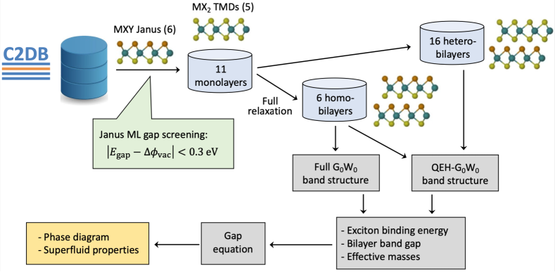
The general approach is sketched in Fig. 1. We begin by searching the C2DB16, 17, 18 for dynamically and thermodynamically stable MXY-Janus materials with a vacuum level difference close in magnitude to the G0W0 band gap of the monolayer eV. Furthermore, for computational reasons we concentrate on materials that have valence band maxima (vbm) and conduction band minima (cbm) at high-symmetry points. Out of the initial pool of 106 MXY Janus materials this leaves us with five candidate materials. In addition to these materials we consider transition metal dichalcogenides (TMDs) in the H-phase that have been synthesized in monolayer form, as well as MoSSe which also has been synthesized but has a too small vacuum level difference to qualify in our initial search. We then consider all possible bilayers which can be formed by combining these monolayers, and compute the band alignments using the Anderson rule. Finally, monolayers that do not form any bilayers with a gap between -0.3 and 0.3 eV are filtered out. This provides us with our final set of 11 monolayer materials that we will consider for further analysis.
We proceed to calculate the equilibrium stacking order and interlayer distance for the homobilayers using a -scan approach (see SI). For the heterobilayers, the interlayer distances are estimated as the average interlayer distances of the corresponding homobilayers (we do not perform explicit DFT calculations for the heterobilayers because of the different in in-plane lattice constants, which would lead to very large simulation cells). We construct all possible bilayers and estimate the band gaps from the G0W0+SOC band gaps of the monolayers including an additional screening correction computed with the G0W0-QEH model 26:
| (1) |
Here the superscript () denotes the electron (hole) layer and are the G0W0 band edges of the monolayers relative to the vacuum level (average vacuum level, , for Janus monolayers). The terms , where are the vacuum levels on the two sides of the sheet, account for the shift in band edges due to the build-in field of Janus monolayers. Finally, , represents the shifts in the monolayer band edges due to the additional dielectric screening stemming from the other layer. The latter is evaluated using the QEH model26. For the six Janus homobilayers, we also perform full G0W0 calculations (Fig. 2), including spin-orbit coupling. These calculations provide very accurate quasiparticle band gaps for this subset of materials (which is the main focus of the article) and serve as benchmarks for the approximate band gaps obtained from Eq. (1). We note that full G0W0 calculations are very challenging for general heterobilayers due to the different in-plane lattice constants.
Using effective masses for the relevant bands (cbm in the electron layer and vbm in the hole layer) obtained from the C2DB and averaged over the and directions, we compute the interlayer exciton binding energies using a Wannier-Mott model
| (2) |
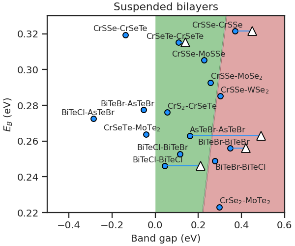
where is the screened electron-hole interaction obtained with the QEH model 19. Upon comparing the binding energy of the lowest exciton with the band gap, we obtain the final list of 16 bilayers for which the exciton binding energies are larger or only slightly smaller than the QP gap (see Fig. 3). These systems are expected to form excitonic insulators and potentially superfluid condensates at low temperatures.
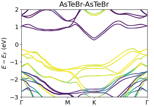
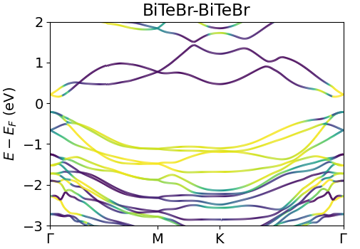
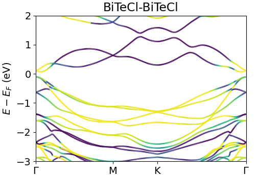
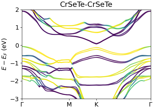
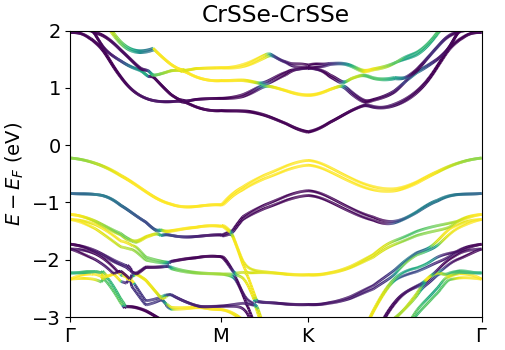
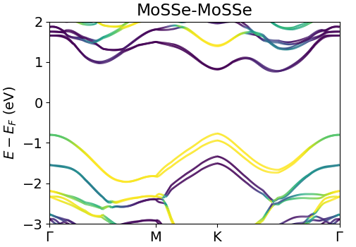
We begin by discussing the G0W0 band structures of the six homobilayers, see Fig. 2. For these materials the size of the band gap is determined by a delicate competition between spin-orbit coupling (SOC), hybridization and screening. While the PBE band gaps are relatively large, the addition of SOC greatly reduce the band gaps and turn the materials with heavy elements into metals. However, inclusion of correlation effects within the G0W0 self-energy approximation increases the size of the band gap again. For accurate estimations of the gaps for these materials it is therefore essential to include both SOC and correlation effects. Monolayer AsTeBr exhibits a small indirect band gap of 0.49 eV while all other materials have direct bandgaps. The color code indicates the layer projection of the corresponding PBE+SOC Bloch states onto the bottom layer. Most of the materials have bands with well defined layer projections, however, for the Bi-compounds the character of the bands is clearly mixed around the -point. A large part of this mixing can be attributed the fact that the PBE+SOC band structure is metallic which yields an increased hybridization between the layers in the PBE+SOC band structure compared to the G0W0 band structure. If the G0W0 wave functions would have been computed self-consistently, as done in quasiparticle self-consistent GW, one would thus expect the hybridization to be reduced and the vbm/cbm states at have more distinct layer projections.
The G0W0 quasiparticle corrections are computed on a Monkhorst-Pack (MP) mesh and interpolated to the band structure path in the Brillouin zone. Non-analytic features in the band structure, such as the V-shape of the conduction band in CrSSe-CrSSe are artifacts of the interpolation and not present in the underlying PBE bandstructures. However, since both the and points are included in the MP-mesh the size of the band gaps are accurate and independent of the interpolation.
The exciton binding energy in Eq. (2) is determined by the effective mass and the screened electron-hole Coulomb interaction. Since the dominant contribution to the density response function comes from interband transitions within the individual monolayers, the magnitude of the attractive electron-hole interaction is essentially determined by the monolayer band gap: if the monolayer gap is large, the screening is correspondingly low and the exciton binding energy will be larger. Thus, the reduction of the band gap in the bilayers, which is driven by out-of-plane dipole of the Janus structures, does not enhance the dielectric screening significantly. This makes it possible to construct small band gap materials with large exciton binding energies and is the key advantage of vdW bilayers for realising excitonic ground states.
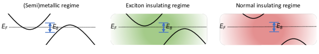
In the left panel of Fig. 3 we show the exciton binding energies, computed with the Wannier-Mott model Eq. (2) as a function of the QP gap for all 16 bilayers. One can identify three distinct regions: (1) The (semi)metallic region (white) with a negative QP gap. (2) The excitonic insulating region (green) where the exciton binding energy is larger than the QP gap. (3) The normal insulating region (red) where the gap is larger than the exciton binding energy. One would expect interesting excitonic phases in the white and green region only, since in the red region spontaneous exciton formation is inhibited by the large band gap. All materials in the green region are expected to have an excitonic insulating ground state, while the materials in the white region can be either normal metals or exciton superfluids at low temperatures depending on the competition between metallic screening and exciton condensation. This will be further analysed using the mean field gap equation.
For the Janus homobilayers we show the band gaps obtained from full G0W0 calculations as white triangles while the G0W0-QEH gaps are shown as blue circles. For vdW heterostructures composed of 2D materials with no out-of-plane dipole, i.e. non-Janus monolayers, the Anderson rule for band alignment typically overestimates the band gap due to neglect of hybridisation effects. 26. Thus, one would expect the full G0W0 band gaps to be smaller than the G0W0-QEH estimates. Looking at Fig. 3 it is evident that this simple picture does not hold for most of the Janus homobilayers considered in this work. The effect is most pronounced for AsTeBr where the G0W0-QEH calculation underestimates the full G0W0 gap by more than 0.3 eV. This surprising result can be understood from nontrivial hybridization effects and incomplete dipole band shifts in the Janus bilayers. In the G0W0-QEH method one assumes that the electric dipoles of the monolayers are unchanged when the bilayer is formed and hence the vacuum level difference of the bilayer should be twice the vacuum level difference of the monolayers. From Table 1 one can see that the vacuum level shift for the six Janus homobilayers () are in general smaller than twice the monolayer shifts (). However, this fact alone is not sufficient to explain the large deviations between the G0W0-QEH and full G0W0 calculations for AsTeBr. For this material the vacuum level difference of the monolayer is 1.7 eV, and half the vacuum level difference of the bilayer is 1.4 eV but the shift of the conduction band between the two layers is only 1.16 eV. Thus, the bands are shifted less than half the bilayer vacuum level difference. The magnitude of this (incomplete) dipole band shift depend on the stacking, and thus the stacking sequence could potentially be used to fine-tune the gap for individual bilayers.
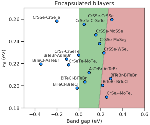
To increase the stability of the bilayers it is often advantageous to encapsulate them in a stable material, such as hexagonal boron nitride (hBN). In the right panel we therefore show the same quantities for bilayers encapsulated in three layers of BN on both sides. As expected the addition of the six hBN layers increases the screening in the materials and therefore reduces the effective electron-hole interactions and thus also the exciton binding energies. However, since the QP gap is also reduced, encapsulation does not change any of the qualitative conclusions in this manuscript. It is interesting to note that the reduction is material dependent so that e.g. the relative ordering in binding energy between BiTeBr-AsTeBr and CrS2-CrSeTe is reversed for the encapsulated bilayers. This further highlights the importance of an ab initio treatment of the screening in these systems.
To investigate the superfluid properties, we combine the QEH model with the recently developed exciton DFT method 27 to solve a superfluid gap equation with ab initio parameters (see supplementary information (SI)). This combination is also interesting from a methods perspective since it shows how the QEH model can be used to compute inputs to general gap-equations and thereby place model studies, such as those in Refs. 28, 29, 8, 30, 31, 32, 33, 34, 35, 36, 37, in a more stringent ab initio framework. This ab initio downfolding method, as well as the standard model treatment is described in the SI.
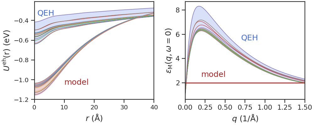
In Fig. 4 we compare the effective electron-hole interaction and the macroscopic dielectric function to the corresponding quantities in the standard model treatment. The screening in the model interaction (red lines) is determined by a single parameter, the static dielectric constant, which is taken to have the value two for a wide range of different materials (see the right panel) 28, 29, 8, 30, 31, 32, 33, 34, 35, 36, 37. Thus, the only material dependent quantity that enters the model interaction is the distance between the electron and hole layers. In contrast, the ab initio calculated dielectric function (blue lines) has both a substantial and material dependence, indicating a pronounced spatial and material dependence in the screening which yields a qualitatively different electron-hole interaction (left panel). It is not only the depth of the potential well that is different between the ab initio and model interaction, but also the relative ordering between the different materials. Therefore a careful treatment of the screening is essential to understand and predict material trends.
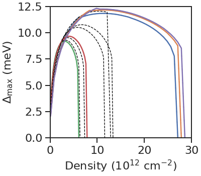
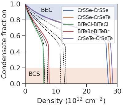
We then proceed to solve the mean-field gap equation (see SI) for all bilayers with direct band gaps where CDW reconstructions are not expected to be associated with spontaneous exciton formation, since the excitons do not carry a finite momentum.38 Superfluidity survives at relatively high electron and hole densities (left panel in Fig. 5), up to 30 cm-2 for the Cr compounds, with the highest cutoff density for bilayer CrSeTe corresponding to a transition temperature K.
The superfluid state is within the mean-field description characterized by the condensate fraction , where and are the Bogiliubov amplitudes in the mean-field model. For the condensate is said to be in the BEC regime of spatially localized electron-hole pairs while for it is said to be in the BCS regime. This characterization is, within the mean-field model, approximate but has shown to be useful for a range of systems39, 33, 32, 30, 31, 27, 30. As can be seen in the middle panel in Fig. 5 the gap collapses in the crossover regime, before the systems have reached the BCS regime.
In this work we use a static mean-field approximation for the self-energy in the gap equation (see SI) and thereby ignore the effect of dynamical screening. In Ref. 27 it was shown that an effective treatment of the frequency dependence beyond the mean-field approximation yield increased cutoff densities and transition temperatures. Similarly, it has been shown that the parabolic approximation to the dispersion tend to underestimate the cutoff densities for TMD heterostructures.31 Since we employ both these approximations the transition temperatures and cut-off densities in this work should be regarded as a lower limit.
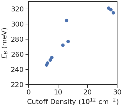
It is interesting to compare the exciton binding energy within the Wannier-Mott model and the superfluid cut-off density within the mean-field gap equation. Since both these quantities in principle are uniquely determined by the effective mass and effective interaction one would naively expect that there would be some correlation between the two quantities. Indeed, as can be seen in the right panel of Fig. 5 there is a correlation between high binding energies and high cut-off densities, albeit not very clear. The reason for the fluctuations is twofold. First, contrary to the superfluid properties, the exciton binding energy does not depend on the electron-electron or hole-hole interactions. Secondly, the metallic screening in the doped systems, which determine the fully screened interaction in the gap equation, depend in a non-trivial way on the single-particle dispersion, superfluid gap and effective interactions through the self-consistency in the gap equation. While the exciton binding energy in the Wannier-Mott model increases for larger effective masses, large effective masses would for a fixed tend to increase the superfluid gap in the gap equation, but for a fixed tend to increase the screening and thereby reduce . Thus it is not sufficient to look at the exciton binding energies in order to determine the superfluid properties of the doped systems.
| Material | ||
|---|---|---|
| CrSSe | -0.826 | -1.334 |
| CrSeTe | -0.783 | -1.18 |
| BiTeCl | 1.547 | 2.807 |
| BiTeBr | 1.204 | 2.229 |
| AsTeBr | 1.716 | 2.863 |
| MoSSe | -0.755 | -1.328 |
To summarize, we propose a new platform for excitonic insulators and exciton superfluidity, namely bilayers of 2D Janus materials. In these systems the out of plane dipole yields a reduced gap in the bilayer compared to the monolayers and it is thus possible to form bilayers with a narrow and ”spatially indirect” band gap from two monolayers with relatively large intrinsic band gaps. We show that the interlayer exciton binding energies in these systems can exceed the bilayer band gap, and therefore one would expect the materials to have an exciton insulating ground state. An analysis of the superfluid properties of the bilayers as a function of electron and hole concentrations shows that superfluid transition temperatures above 50 K are possible. The most promising compounds for exciton superfluidity are bilayers based on the chromium-chalcogenide MXY Janus materials CrSSe and CrSeTe.
The Supplemental information includes all relevant properties of the monolayer building blocks and bilayer structures as well as an account of the z-scan approach used to determine the interlayer distance. We also include a detailed discussion of the gap equation used to model the superfluid properties and a motivation for the ab initio downfolding scheme used to determine the effective interaction in the gap equation. Finally, the computational parameters are stated.
F. N. would like to acknowledge discussions with Chin-Shen Ong at Uppsala University in the initial phases of this project. The authors acknowledge funding from the European Research Council (ERC) under the European Union’s Horizon 2020 research and innovation program Grant No. 773122 (LIMA) and the Villum Investigator Grant No. 37789 supported by VILLUM FONDEN. F.N has received funding from the European Union’s Horizon 2020 research and innovation program under the Marie Skłodowska-Curie grant agreement No. 899987. (EuroTechPostdoc2).
References
- Mott 1961 Mott, N. F. The transition to the metallic state. Philos. Mag. 1961, 6, 287–309
- Halperin and Rice 1968 Halperin, B.; Rice, T. Possible anomalies at a semimetal-semiconductor transistion. Rev. Mod. Phys. 1968, 40, 755
- Kogar et al. 2017 Kogar, A.; Rak, M. S.; Vig, S.; Husain, A. A.; Flicker, F.; Joe, Y. I.; Venema, L.; MacDougall, G. J.; Chiang, T. C.; Fradkin, E. et al. Signatures of exciton condensation in a transition metal dichalcogenide. Science 2017, 358, 1314–1317
- Jia et al. 2022 Jia, Y.; Wang, P.; Chiu, C.-L.; Song, Z.; Yu, G.; Jäck, B.; Lei, S.; Klemenz, S.; Cevallos, F. A.; Onyszczak, M. et al. Evidence for a monolayer excitonic insulator. Nat. Phys. 2022, 18, 87–93
- Sun et al. 2022 Sun, B.; Zhao, W.; Palomaki, T.; Fei, Z.; Runburg, E.; Malinowski, P.; Huang, X.; Cenker, J.; Cui, Y.-T.; Chu, J.-H. et al. Evidence for equilibrium exciton condensation in monolayer WTe2. Nat. Phys. 2022, 18, 94–99
- Morita et al. 2022 Morita, Y.; Yoshioka, K.; Kuwata-Gonokami, M. Observation of Bose-Einstein condensates of excitons in a bulk semiconductor. Nat. Commun. 2022, 13, 1–9
- Mazza et al. 2020 Mazza, G.; Rösner, M.; Windgätter, L.; Latini, S.; Hübener, H.; Millis, A. J.; Rubio, A.; Georges, A. Nature of symmetry breaking at the excitonic tnsulator transition: . Phys. Rev. Lett. 2020, 124, 197601
- Gupta et al. 2020 Gupta, S.; Kutana, A.; Yakobson, B. I. Heterobilayers of 2D materials as a platform for excitonic superfluidity. Nat. Commun. 2020, 11, 1–7
- Liu et al. 2017 Liu, X.; Watanabe, K.; Taniguchi, T.; Halperin, B. I.; Kim, P. Quantum Hall drag of exciton condensate in graphene. Nat. Phys. 2017, 13, 746–750
- Li et al. 2017 Li, J.; Taniguchi, T.; Watanabe, K.; Hone, J.; Dean, C. Excitonic superfluid phase in double bilayer graphene. Nat. Phys. 2017, 13, 751–755
- Burg et al. 2018 Burg, G. W.; Prasad, N.; Kim, K.; Taniguchi, T.; Watanabe, K.; MacDonald, A. H.; Register, L. F.; Tutuc, E. Strongly enhanced tunneling at total charge neutrality in double-bilayer graphene- heterostructures. Phys. Rev. Lett. 2018, 120, 177702
- Ma et al. 2021 Ma, L.; Nguyen, P. X.; Wang, Z.; Zeng, Y.; Watanabe, K.; Taniguchi, T.; MacDonald, A. H.; Mak, K. F.; Shan, J. Strongly correlated excitonic insulator in atomic double layers. Nature 2021, 598, 585–589
- Zhang et al. 2017 Zhang, J.; Jia, S.; Kholmanov, I.; Dong, L.; Er, D.; Chen, W.; Guo, H.; Jin, Z.; Shenoy, V. B.; Shi, L. et al. Janus monolayer transition-metal dichalcogenides. ACS Nano 2017, 11, 8192–8198, PMID: 28771310
- Hajra et al. 2020 Hajra, D.; Sailus, R.; Blei, M.; Yumigeta, K.; Shen, Y.; Tongay, S. Epitaxial synthesis of highly oriented 2D Janus Rashba semiconductor BiTeCl and BiTeBr layers. ACS Nano 2020, 14, 15626–15632, PMID: 33090763
- Riis-Jensen et al. 2018 Riis-Jensen, A. C.; Pandey, M.; Thygesen, K. S. Efficient charge separation in 2D Janus van der Waals structures with built-in electric fields and intrinsic p–n doping. J. Phys. Chem. C 2018, 122, 24520–24526
- Haastrup et al. 2018 Haastrup, S.; Strange, M.; Pandey, M.; Deilmann, T.; Schmidt, P. S.; Hinsche, N. F.; Gjerding, M. N.; Torelli, D.; Larsen, P. M.; Riis-Jensen, A. C. et al. The computational 2D materials database: high-throughput modeling and discovery of atomically thin crystals. 2D Mater. 2018, 5, 042002
- Gjerding et al. 2021 Gjerding, M. N.; Taghizadeh, A.; Rasmussen, A.; Ali, S.; Bertoldo, F.; Deilmann, T.; Knøsgaard, N. R.; Kruse, M.; Larsen, A. H.; Manti, S. et al. Recent progress of the computational 2D materials database (C2DB). 2D Mater. 2021, 8, 044002
- 18 Computational 2D materials database (C2DB). \urlhttps://cmr.fysik.dtu.dk/c2db/c2db.html, Accessed: 2022-10-01
- Andersen et al. 2015 Andersen, K.; Latini, S.; Thygesen, K. S. Dielectric genome of van der Waals heterostructures. Nano Lett. 2015, 15, 4616–4621
- Guo et al. 2022 Guo, H.; Zhang, X.; Lu, G. Tuning moiré excitons in Janus heterobilayers for high-temperature Bose-Einstein condensation. Sci. Adv. 2022, 8, eabp9757
- Anderson 1960 Anderson, R. Germanium-gallium arsenide heterojunctions. IBM J. Res. Dev. 1960, 4, 283–287
- Mortensen et al. 2005 Mortensen, J. J.; Hansen, L. B.; Jacobsen, K. W. Real-space grid implementation of the projector augmented wave method. Phys. Rev. B 2005, 71, 035109
- Enkovaara et al. 2010 Enkovaara, J.; Rostgaard, C.; Mortensen, J. J.; Chen, J.; Dułak, M.; Ferrighi, L.; Gavnholt, J.; Glinsvad, C.; Haikola, V.; Hansen, H. et al. Electronic structure calculations with GPAW: a real-space implementation of the projector augmented-wave method. J. Condens. Matter Phys. 2010, 22, 253202
- Hüser et al. 2013 Hüser, F.; Olsen, T.; Thygesen, K. S. Quasiparticle GW calculations for solids, molecules, and two-dimensional materials. Phys. Rev. B 2013, 87, 235132
- Latini et al. 2017 Latini, S.; Winther, K. T.; Olsen, T.; Thygesen, K. S. Interlayer excitons and band alignment in MoS2/hBN/WSe2 van der Waals heterostructures. Nano Lett. 2017, 17, 938–945
- Winther and Thygesen 2017 Winther, K. T.; Thygesen, K. S. Band structure engineering in van der Waals heterostructures via dielectric screening: the GW method. 2D Mater. 2017, 4, 025059
- Nilsson and Aryasetiawan 2021 Nilsson, F.; Aryasetiawan, F. Effects of dynamical screening on the BCS-BEC crossover in double bilayer graphene: Density functional theory for exciton bilayers. Phys. Rev. Mat. 2021, 5, L050801
- Conti et al. 2023 Conti, S.; Perali, A.; Hamilton, A. R.; Milošević, M. V.; Peeters, F. m. c. M.; Neilson, D. Chester supersolid of spatially indirect excitons in double-layer semiconductor heterostructures. Phys. Rev. Lett. 2023, 130, 057001
- Pascucci et al. 2022 Pascucci, F.; Conti, S.; Neilson, D.; Tempere, J.; Perali, A. Josephson effect as a signature of electron-hole superfluidity in bilayers of van der Waals heterostructures. Phys. Rev. B 2022, 106, L220503
- Conti et al. 2020 Conti, S.; Van der Donck, M.; Perali, A.; Peeters, F. M.; Neilson, D. Doping-dependent switch from one- to two-component superfluidity in coupled electron-hole van der Waals heterostructures. Phys. Rev. B 2020, 101, 220504
- Conti et al. 2020 Conti, S.; Neilson, D.; Peeters, F. M.; Perali, A. Transition Metal Dichalcogenides as Strategy for high temperature electron-hole superfluidity. Condens. Matter. 2020, 5
- Conti et al. 2019 Conti, S.; Perali, A.; Peeters, F. M.; Neilson, D. Multicomponent screening and superfluidity in gapped electron-hole double bilayer graphene with realistic bands. Phys. Rev. B 2019, 99, 144517
- Conti et al. 2017 Conti, S.; Perali, A.; Peeters, F.; Neilson, D. Multicomponent electron-hole superfluidity and the BCS-BEC crossover in double bilayer graphene. Phys. Rev. Lett. 2017, 119, 257002
- Perali et al. 2013 Perali, A.; Neilson, D.; Hamilton, A. R. High-temperature superfluidity in double-bilayer graphene. Phys. Rev. Lett. 2013, 110, 146803
- Zarenia et al. 2014 Zarenia, M.; Perali, A.; Neilson, D.; Peeters, F. Enhancement of electron-hole superfluidity in double few-layer graphene. Sci. Rep. 2014, 4, 1–6
- Lozovik et al. 2012 Lozovik, Y. E.; Ogarkov, S.; Sokolik, A. Condensation of electron-hole pairs in a two-layer graphene system: Correlation effects. Phys. Rev. B 2012, 86, 045429
- De Palo et al. 2002 De Palo, S.; Rapisarda, F.; Senatore, G. Excitonic condensation in a symmetric electron-hole bilayer. Phys. Rev. Lett. 2002, 88, 206401
- Jiang et al. 2018 Jiang, Z.; Li, Y.; Zhang, S.; Duan, W. Realizing an intrinsic excitonic insulator by decoupling exciton binding energy from the minimum band gap. Phys. Rev. B 2018, 98, 081408
- Neilson et al. 2014 Neilson, D.; Perali, A.; Hamilton, A. R. Excitonic superfluidity and screening in electron-hole bilayer systems. Phys. Rev. B 2014, 89, 060502