Decagonal Sn clathrate on -Al-Ni-Co
Abstract
Decagonal quasiperiodic ordering of Sn thin film on -Al-Ni-Co is shown based on scanning tunneling microscopy (STM), low-energy electron diffraction and density functional theory (DFT). Interestingly, the decagonal structural correlations are partially retained up to a large film thickness of 10 nm grown at a 16510 K. The nucleation centers called “Sn white flowers” identified by STM at submonolayer thickness are recognized as valid patches of the decagonal clathrate structure with low adsorption energies of the SnWF motifs. Due to the excellent lattice matching (to within 1%) between columns of Sn dodecahedra in the clathrate structure and pentagonal motifs at the -Al-Ni-Co surface, the interfacial energy favors clathrate over the competing Sn crystalline forms. DFT study of the Sn/Al-Ni-Co composite model shows good mechanical stability, as shown by the work of separation of Sn from Al-Ni-Co slab that is comparable to clathrate self-separation energy. The relaxed surface terminations of the R2T4 clathrate approximant are in self-similarity correspondence with the motifs observed in the STM images from monolayer to thickest Sn film.
I Introduction
Quasicrystals show sharp diffraction spots although they do not have translational long range order and rather possess forbidden rotational symmetries. In addition to intermetallic alloys [1, 2], quasicrystallinity has also been observed in various forms such as colloidal systems [3], binary nanoparticles super lattices [4], molecular assemblies [5, 6], chalcogenides [7], twisted bilayer graphene [8, 9] and even in naturally occurring minerals [10]. Quasicrystals are fascinating, especially due to their unusual physical properties such as low specific heat, low thermal and electrical conductivities, and low friction [11, 12, 13]; as well as evidence of Anderson localization [14], demonstration of pseudogap at the Fermi level [15], and recent prediction of topological states [16, 17].
The basic entities that are known to form quasicrystals are clusters such as pseudo-Mackay and Bergman clusters [18]. Crystalline structures with clusters entities, for instance, clathrates, somewhat resemble the clusters that form the quasicrystals. The most straightforward rationalization of the bulk clathrate structure is via the network of its cage centres [19, 20]. Polytetrahedral order [21, 22] is the basis of the crystalline Frank-Kasper phases [19, 20, 23] and has been used in order to realize the structure of quasicrystals [24, 25, 26]. Materials exhibiting clathrate structure [27, 28, 29, 30, 31, 32, 33] have become a subject of interest due to their optical and thermoelectric properties [34, 35], as well as due to their potential for application [36, 37]. Guest-free Si [38] and Ge [39] clathrates have wide quasi-direct band gaps that is important for photovoltaic applications, and Sn with guest atoms has shown clathrate structures [40].
Since the last decade, Sn films have attracted considerable attention because of their interesting electronic properties [41, 42, 43, 44, 45, 46]. In particular, in its single layer honeycomb structure (stanene), Sn has been shown to exhibit topological properties [47, 48, 49]. In a recent advancement towards achieving elemental quasicrystal, we have shown using scanning tunneling microscopy (STM), low energy electron diffraction (LEED), and density functional theory (DFT) that Sn can grow quasiperiodically up to about 4 nm thickness with a clathrate structure on -Al-Pd-Mn substrate [50]. The clathrate quasiperiodic structure nucleates on -Al-Pd-Mn because of an excellent matching (within 1%) of the cage-cage linkage length in Sn clathrates (1.26 nm) with the pseudo-Mackay cluster-cluster separations in -Al-Pd-Mn (1.255 nm).
In the present study, we explore the growth of Sn films on decagonal ()-Al-Ni-Co quasicrystal with a motivation to demonstrate the generality of the clathrate quasiperiodic structure of Sn. -Al-Ni-Co has a different structure compared to -Al-Pd-Mn: the former comprises of decagonal quasiperiodic planes, but exhibits translational periodicity along the ten fold (10f) axis with an inter-planar distance of approximately 0.2 nm [51]. The structure of -Al-Ni-Co has not been solved experimentally until date, but several models have been proposed in literature [52, 53, 54]. Sugiyama et al. determined the structure of the W approximant of -Al-Ni-Co (W-Al-Ni-Co) using x-ray diffraction, and showed that it is closely related to -Al-Ni-Co [54]. The 10f -Al-Ni-Co surface was modelled by Krajčí et al. [55] based on W-Al-Ni-Co as alternating flat (A) and puckered (B) atomic layers perpendicular to the periodic axis along the direction. The surface energy of -Al-Ni-Co is reported to be 1.17 J/m2 [56], while that of Sn is 0.71 J/m2 [57]. Thus, from surface energy considerations, Sn is expected to wet the -Al-Ni-Co surface. However, Sn deposition on -Al-Ni-Co has been scarcely studied in literature. Shimoda reports a pseudomorphic monolayer of quasiperiodic Sn on -Al-Ni-Co using RHEED, XPS, and STM [58]. For depositing Sn, these authors however pre-coated the backside of the specimen with Sn and then with heating Sn diffused and spread over to the front side. This method precludes possibility of growing thicker Sn films, since it requires high temperatures.
Although there has been four decades of active research on quasicrystals, elemental quasicrystals have remained elusive so far. In this paper, we show the formation of decagonal Sn thin film (thickness 1 nm) on a 10f -Al-Ni-Co surface based on LEED and STM. The decagonal structural correlations are partially retained up to a large film thickness of 10 nm. The quasiperiodic motifs observed from STM up to 10 nm thick Sn film are in good self-similarity correspondance with the decagonal clathrate R2T4 approximant model of Sn calculated by DFT that show relaxed penta-hole and penta-cap terminations. The “Sn white flowers” (SnWFs) identified by STM after submonolayer Sn deposition are the nucleation centers of the decagonal clathrate structure with low adsorption energies. Due to the excellent lattice matching (to within 1%) between Sn clathrate and the -Al-Ni-Co surface, the interfacial energy favors the clathrate. DFT study of the Sn/Al-Ni-Co composite model shows good mechanical stability, as shown by the work of separation of Sn from Al-Ni-Co slab that is comparable to clathrate self-separation energy. The paper is organized as follows: We provide experimental evidence of decagonal quasicrystallinity in Sn thin films using STM and LEED (subsection III.1) and the evidence of decagonal structural correlations in the thick films is provided in subsection III.2. Thereafter, we provide a theoretical model for a decagonal clathrate structure of Sn from DFT (subsection III.3). A piece of evidence supporting the clathrate decagonal model is a detailed analysis of the nucleation supported by the STM results that are discussed in subsection III.4. Next, in subsection III.5, we consider a Sn/-Al-Ni-Co R2T4 approximant composite model to study the adlayer-substrate interaction with DFT. Finally, in subsection III.6 we define the motifs based on our theoretical model and show that these are observed from STM and a sizable contagious region of the image for the 10 nm thick film is in good agreement with the theory.
II Methods
The STM experiments were carried out in a variable temperature STM system from Scientaomicron at a base pressure of 510-11mbar. The experiments were performed using an electrochemically etched polycrystalline tungsten tip that was cleaned in situ by Ar+ ion sputtering and voltage pulse method. The images were recorded in the constant current mode with the sample at ground potential for various sample bias voltages and are shown after low-pass Fourier transform filtering. The analysis was performed using the SPIP software. The zero of the color scale for all the STM images corresponds to the bearing height i.e. the most frequently occurring height. The root mean square roughness () is defined as the square root of the sum of squares of each height value () at each pixel coordinate (, ) in the () pixel dataset given by .
The LEED equipment from OCI Vacuum Microengineering has a retractable four grid rear view optics, and the patterns were recorded with a digital camera in nearly normal incidence geometry at 1 eV step of the beam energy () that was varied from 30 to 200 eV. The I-V curves were determined for a spot by calculating its intensity for each in a window of fixed size with the spot in its middle. An averaging was performed for all the symmetry equivalent spots. Image J software [59] was used to invert the gray color scale after applying the auto contrast option to adjust the brightness and intensity.
Monocrystalline -Al-Ni-Co quasicrystal was grown from a high temperature ternary melt [60] and separated from the excess liquid via centrifuging [61]. -Al-Ni-Co was mounted on a specially fabricated cooling sample plate made of molybdenum. A smooth and clean -Al-Ni-Co surface was obtained by cycles of 0.5-1.5 keV Ar+ ion sputtering and followed by annealing at 1043 K in the UHV chamber for 4 hr [62]. Sn of 99.99% purity was evaporated using a water-cooled Knudsen evaporation cell [63] equipped with a shutter that is operated manually using a rotary feedthrough. The temperature of the cell used for deposition was 1163 K and this was measured by a K-type thermocouple placed at the outside bottom of the pyrolytic boron nitride crucible. The deposition was performed at an angle of 70∘ from the surface normal, and the pressure of the chamber during the deposition was 510-10 mbar. The substrate surface was freshly prepared for both 0.2 ML and 1 ML Sn deposition. For the thick films with varying from 3 to 37 min, the deposition was sequential. For the depositions at 16510 K, the LEED was performed at the same temperature while STM was performed at 80 K.
Structural optimization study of the Sn surface terminations and reconstructions, as well as Sn/Al-Ni-Co model relaxations, have been performed using plane-wave DFT code Vienna ab initio Simulation Package (VASP) [64]. We used projector augmented wave potentials [65] in the PW91 generalized gradient approximation [66]. Default energy cutoff () 103.3 eV preset by “accurate” calculational setup turned out to be sufficient considering energy differences between different samples: out of the four samples examined for convergence, change of the from = 103.3 to 300 eV was 0.3 meV/atom, certainly well below other unaccounted systematic inaccuracies. The -point meshes were converged to comparable change in upon increasing mesh density.
III Results and Discussion
III.1 Quasiperiodicity of Sn thin films ( 1 nm) on -Al-Ni-Co
III.1.1 Monolayer Sn:
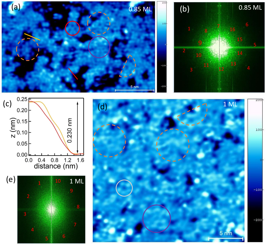
An STM topography image of 0.85 ML Sn on -Al-Ni-Co in Fig. 1(a) indicates possible quasiperiodicity of the adlayer through sharp 10f spots in its fast Fourier transform (FFT) in Fig. 1(b) that has ∼85% contribution from the adlayer. The FFT shows two sets of 10f spots. The spots are numbered such that the corresponding intensity profiles along the tangential direction can be shown. In Fig. S1(a,b) of the supplemental material (SM) [67], each intensity profile shows a peak at the position of the spot and thus all the spots are unambiguously identified. The ratio of their radii is 1.920.03, which is close to = 1.90, where is the golden mean given by = (1+)/2= 1.618. is the ratio of the side of a regular pentagon and the distance from its center to the vertex; it is related to by = = 1.176 [68, 69]. The outer set of spots is rotated by 18∘ with respect to the inner set. The height profiles taken along the red and yellow lines from the STM image [Fig. 1(a)] are plotted in Fig. 1(c). These show the difference of the average corrugation (the double-sided arrow) of the Sn monolayer islands (light blue regions) and the substrate (dark), which is the thickness of the latter under the assumption that the electronic height is equal to the geometric height. After averaging over more than 30 such profiles from different parts of the image as in our earlier work [70], we find the thickness of the Sn monolayer island to be 0.230.02 nm.
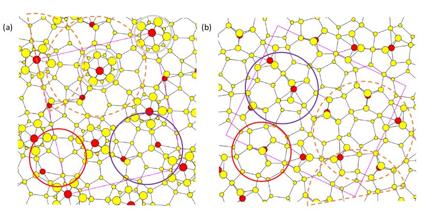
In Fig. 1(d), STM topography image of nearly one monolayer (0.97 ML) is displayed. The 10f symmetry of the spots observed in the FFT [Fig. 1(e)] and their intensity profiles along the tangential direction are shown in Fig. S1(c) of SM [67]. Two adjacent spots subtend an angle of 36∘2∘ at the center demonstrating the quasiperiodic nature of the Sn monolayer. Different quasiperiodic motifs of Sn such as wheel, crown, pentagon, and polygon assembly are highlighted in Figs. 1(a,d). These motifs are defined on the basis of the relaxed surface of the clathrate structural model calculated by DFT (see subsection III.6).
We find that the growth of Sn films of larger thickness beyond a monolayer is difficult at 300 K because of very low sticking coefficient and large diffusivity. On the other hand, at liquid helium temperatures, the diffusivity would be too low for an ordered growth. So, we have used an intermediate lower temperature (LT) of 16510K for growing Sn films thicker than a monolayer. LT is in fact a stringent requirement for growing Sn thick films.
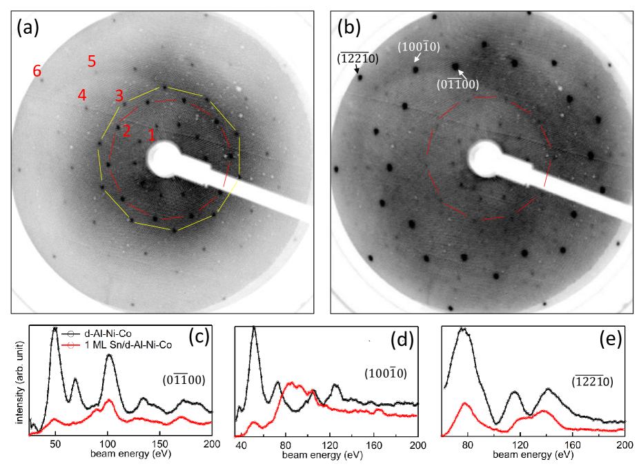
The quasiperiodicity of the Sn monolayer at LT is evident from several sets of 10f spots in the LEED pattern (numbered 1-6) at an angular separation of 36∘ [Fig. 2(a)]. The ratios of the radii of the outer sets and the innermost set are related by powers and product of and , as shown in Table SI of SM [67]. The intensity profile through some of the spots (numbered 1-10) of both the substrate and the Sn adlayer is shown in Fig. S2 of SM [67]. To be noted is that the position of the spots change with (Fig. S3 of SM [67]). In particular, for = 100 eV, the prominent intensities are seen at a higher reciprocal distance compared to the substrate in contrast to = 55 eV (Fig. 2). Note that the LEED pattern is significantly different from the substrate: e.g. in Fig. 2(a), an extra set of diffraction spots (highlighted by yellow lines) is observed, which is not visible in -Al-Ni-Co in Fig. 2(b). Also, the set of spots highlighted by red lines is more intense compared to the substrate. The shape of the intensity versus voltage (I-V) curves for the LEED spots as a function of depends sensitively on the surface structure [71, 72, 73, 74]. A comparison of the I-V curves of monolayer Sn in Figs. 2(c-e) for three different set of spots shows that these are quite different from the substrate. For example, for the (000) spot, the substrate peak at 73 eV is completely absent, while the most intense peak at 52 eV is largely suppressed and shifted below 50 eV. It is a similar situation for the (1000) spot below 80 eV, and furthermore the 126 eV substrate peak is absent. For the (0) spot, the two peaks of the substrate at 116 and 141 eV move closer in the Sn layer and fill up the dip at 128 eV. The above discussed differences in the LEED evident from the patterns as well as the I-V curves indicate that although the Sn monolayer exhibits decagonal symmetry, it has a different structure portraying a non-pseudomorphic growth.
A comparison of the STM topography image of the Sn monolayer at LT (Fig. S4(a) of SM [67]) with that at 300 K [Fig. 1(d)] shows that uniform wetting occurs at LT and their roughness is almost similar (= 0.0530.004 nm at LT, whereas it is 0.0460.004 nm at 300 K). Motifs such as wheel, crown and polygon assembly are also observed [Figs. S4(b-d) [67]].
III.1.2 Sn film of 0.9 nm thickness:
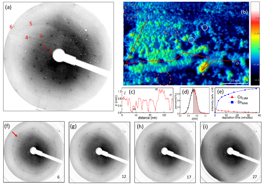
In Fig. 3(a), the = 3 min LEED pattern shows six sets of 10f spots at angular separation of about 36∘ that are similar to the Sn monolayer. In Fig. S5(a) of SM [67], the spots are numbered and the corresponding intensity profiles are shown in Fig. S5(b-e) [67]. A video file named as “0.9nm” in the SM [67] shows that the intensities of all the spots in each set remain similar for the whole range of i.e. 20150 eV. The above observations establish that this film exhibits decagonal symmetry. For comparison, the LEED video corresponding to the monolayer is also uploaded as “monolayer” in the SM [67]. The ratios of the radii of the outer sets and the innermost set are related by powers and product of and , as shown in Table SII of SM [67].
A STM topography image of this film in Fig. 3(b) shows an increase in roughness with being 0.15 nm. Motifs highlighted by dashed orange and gray circles exhibit resemblance with the monolayer. The crown and the wheel motifs [zoomed and compared with our theoretical model in Figs. S6(a,b)] are similar to that of the monolayer shown in Figs. 16(a,b). The STM image provides a measure of its thickness from the height profile along the line named as lmno i.e. the red line in Fig. 3(a). It shows that there is considerable variation in the thickness and the maximum local height is 1.2 nm around with respect to the region around that has lowest height [Fig. 3(c)]. The height histogram of Fig. 3(d) is a nearly symmetric peak with maximum at 0.65 nm with 50% area (red shaded) having a thickness 0.65 nm. So, the peak position (0.65 nm) is considered to be the average thickness of the film referenced to . Since the -Al-Ni-Co surface is uniformly wetted by a monolayer of Sn, the thickness around should be at least that of a monolayer i.e. 0.23 nm. Thus, the average thickness of the intermediate layer is at least 0.88 nm (0.65+ 0.23 nm) i.e. ∼0.9 nm.
III.2 Sn thick films on -Al-Ni-Co
III.2.1 Sn deposition for 627 min :
Here, we first establish that there is a continuous increase of the average thickness of the Sn film with . This is shown by the Sn MNN Auger signal that increases monotonically [Fig. 3(e)]. Concomitantly, the substrate related Co LMM Auger signal decreases and at = 37 min, it is almost in the noise level [Fig. 3(e)].
In Fig. 3(f), the LEED pattern for = 6 min with a thickness of 2 nm shows five sets of decagonal spots. The (1000) spots also develop a continuous ring (red arrow), although the sets of spots at lower reciprocal distances do not show any such ring. At = 12-27 min [Figs. 3(g-i)], the spots at the lower reciprocal distances are diminished in intensity, whereas both the decagonal spots and the ring related to (1000) are visible. The significance of the ring is discussed in the next subsection (III B 2). The video files as a function of corresponding to Figs. 3(f-i) named as “6min”, “12min”, “17min”, and “27min”, respectively are provided in the SM [67].
III.2.2 Thickest (10 nm) Sn film :
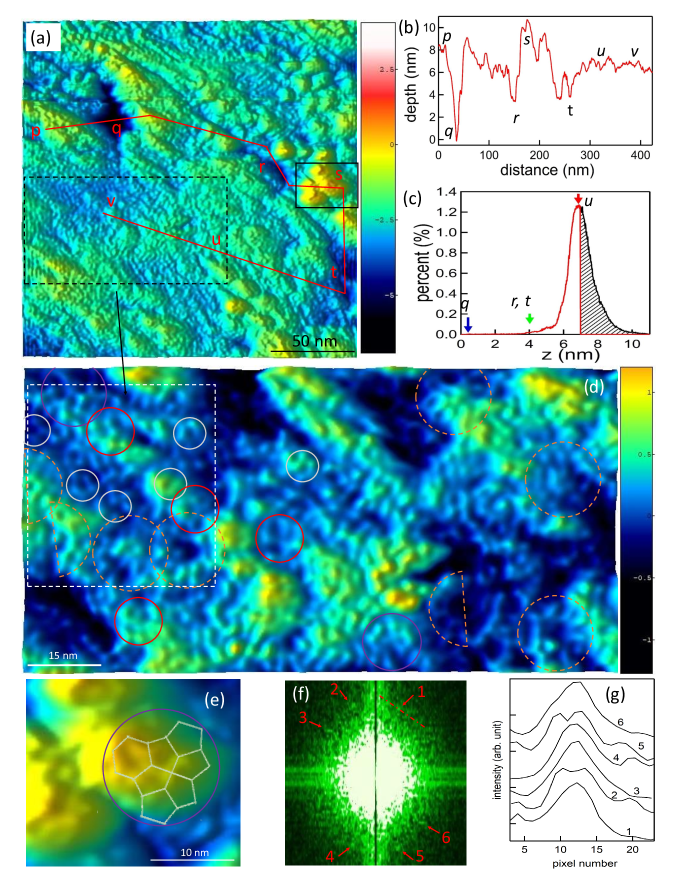
A large area STM topography image of a thick Sn film grown on -Al-Ni-Co with = 37 min is shown in Fig. 4(a). The height profile in Fig. 4(b) along [red line in Fig. 4(a)] shows that the region around (highlighted by a black rectangle) has a height of about 10 nm with respect to the local minimum region (e.g., region ). However, the heights exhibit substantial lateral variation e.g. around it is 8 nm, whereas a large region around it is 6-7 nm. Thus, the film exhibits a rugged topography that resembles a geographical undulated “hilly terrain”, where a valley represents the local minimum region (), but the bottom of the valley is at a larger height compared to the “sea level” (i.e., the monolayer). To find the thickness of the Sn film at , we consider a uniform Sn deposition with time: thus for = 37 min the estimated thickness at region is about 2.8 nm. This is estimated on the assumption that for the 0.9 nm film grown with = 3 min, the thickness of the minimum region [m in Fig. 3(b)] is one monolayer (0.23 nm). This estimate of the thickness at is consistent with the fact that the substrate Co Auger signal is almost completely suppressed [Fig. 3(e)]. Note that the added area of regions having thickness close to is only 1-2% of the total area. In Fig. 4(c), the height histogram shows a nearly symmetric peak centered at 7 nm (50 of the area shown by black shading has a thickness 7) that is taken as the average thickness with respect to whose thickness is 2.8 nm. Thus, by adding these two numbers, the total average thickness of the thickest Sn film studied by us turn out to be 100.5 nm.
This film has an order of magnitude larger roughness (= 0.54 nm) compared to the monolayer (= 0.053). In spite of this, the characteristic motifs similar to those observed for the thin films are observed [Fig. 4(d)]. The largest thickness region around portrays an elevated dome highlighted by a violet circle in Fig. 4(e), whose average base diameter is 123 nm, as shown by the histogram in Fig. S7 of SM [67]. It is interesting to note that a quasiperiodic motif is observed on the dome, which partially resembles a polygon assembly (see III.6).
In Fig. 4(f), an averaged FFT of the STM images shows occurrence of 6 spots (#1– #6). Their presence is established in Fig. 4(g) by the intensity profiles across the spots along the tangential direction (as shown for spot 1 by a red dashed line). It may be noted that a notional circle joining the spots is distorted to an oval shape, which could be related to the thermal drift in the STM measurement [50]. The spots are weaker compared to that of the monolayer, as also in the case of the LEED spots shown in Fig. 5. Possible reasons for this could be the intrinsic puckered nature of the film, as shown in III.6, stochastic processes, competing disorder, and the roughness of the film due to growth at LT that degrades the quality of the STM images.
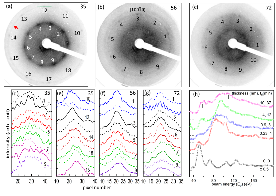
LEED investigation of the Sn thick film shows 10f spots highlighted by numbering in Figs. 5(a-c), and their intensity profiles are shown in Figs. 5(d-g). A peak representing each spot is clearly observed with respect to the background, and these decagonal spots provide the evidence of the decagonal symmetry in the thick film. At = 35 eV, the outer set of spots are 18∘ rotated with respect to the inner spots [Fig. 5(a)], and ratio of the radii of the outer spots (10–18) and the inner spots (1–9) is 1.86 ( = 1.9). Any possibility of crystalline domains [75] or presence of approximant phases are ruled out because there are no extra spots or splitting of the spots at any (also see the video file named “10nm” in SM [67]). All the spots move towards the (0,0) spot as increases. It may be noted that besides the discrete spots, as in Figs. 3(f-i), a weak continuous ring that joins the (1000) spots is observed [red arrow in Fig. 5(a)] possibly indicating a rotational degree of freedom between the decagonal structures. The latter could probably be related to its clathrate structure, since Engel proposed possibility of random tiling quasicrystal in clathrates that are axially symmetric [76]. However, this would mean that the intermediate regions connecting the decagonal structures would not be periodic. In subsection III.6 (Fig. 17), we discuss this further by comparing the STM image of the 10 nm film with DFT based decagonal clathrate model that is presented in the subsection (III.3).
The I-V curve for the (1000) spot of the Sn thick film exhibits peaks centered at = 58, 95, and 110 eV as shown by the ticks in the top curve of Fig. 5(h). The peak positions are similar to the 4 nm film (= 12 min), although in the latter, the 95 eV peak is somewhat more intense. The peaks in I-V curves of the thin films [0.23 nm i.e. one monolayer and 0.9 nm in Fig. 5(h)], although have nearly similar shape, are shifted by about 8-15 eV towards lower , which implies a possible change in the lateral length scale [77]. Finally, it is noteworthy that the shape of the I-V curves of the Sn films of different thicknesses starting from the monolayer (0.23 nm) are completely different from that of the substrate that has the peaks at = 52, 73, 106, and 125 eV. This shows that the structure of the Sn films, although decagonal, is different from the substrate.
III.3 Model for the atomic structure, surface termination and DFT-optimized reconstruction of the Sn decagonal clathrate
The low-temperature stable phase of Sn, the -Sn in cubic diamond -bonded structure (“gray tin”), transforms to metallic and denser tetragonal -Sn (“white tin”) above 286 K. The clathrate structures are also -bonded by grouping atoms around point centers into empty cages. In our experiments, the thick Sn film was deposited at 165K, deeply in the stability range of -bonded structures. At zero temperature, the cohesive energy differences of the alternative candidates for stability relative to -Sn obtained from DFT are: +46 meV/atom for the -Sn and +29 meV/atom for the face centered cubic clathrate type II (that contains highest fraction of the smallest dodecahedral cages and has lowest energy out of all clathrates, see Ref. 50 for a discussion about type II and III clathrates). Given the fact that the -Al-Ni-Co substrate surface exhibits excellent match with the clathrate structure (see subsection III.4), nucleation of the -Sn and -Sn structures must be suppressed due to the surface structure incompatibility. Moreover, the low deposition temperature is another disadvantage factor for metallic -Sn. Presumably, an amorphous Sn phase might compete with the magic clathrate interfacial compatibility with -Al-Ni-Co. But while Si or Ge amorphous phases can be prepared easily and they have apparently -bonding nature, reports on amorphous Sn are very scarce, and to our knowledge literature does not report -bonded, low–density amorphous Sn phase that might be a hypothetical competitor at low temperatures.
In addition to these general considerations, the clearly recognizable decagonal symmetry of the LEED pattern from the thick Sn layer rules out any of the alternatives considered above. The role of the substrate is to prevent possible formation of crystalline Sn structures. In the following, we develop detailed theoretical – although indirect – support for decagonal clathrate as the only plausible candidate model structure for the thick Sn film. In the following subsection (III.3.1), we argue how the decagonal clathrate follows from the dual relationship (where connecting the centers of the faces of one structure gives the other e.g., an icosahedron gives a dodecahedron) between the Frank–Kasper and the clathrate structures [19, 20, 78]. We then review the decoration prescription associating the precise bulk clathrate atomic structure of Sn with two-dimensional geometry of the R-T tilings. The next subsection III.3.2 discusses the decagonal clathrate surface terminations, and finally subsection III.3.3 reports on the DFT–guided energy optimization of such terminations by adding adatoms at specific locations to neutralize the energy cost of the unsaturated bonds at the surface.
III.3.1 Tiling description of the decagonal clathrate:
Frank and Kasper [19, 20] pointed out that the network of clathrate cage centers forms tetrahedrally close-packed (TCP) geometry, and suggested that new clathrate structures can be derived from the known examples of the metallic structural family. Following this route, a decagonal TCP quasicrystal structure [79] can be dual-transformed into decagonal clathrate [50]. The common geometrical framework of the two related structural families is decagonal tiling of rectangles and isosceles triangles (R-T tiling hereafter).
The decagonal R-T tiling – common geometry for metallic TCP structures or clathrates – consists of isosceles triangles (T) with two shorter sides with length and a longer side = and rectangles (R) with aspect ratio of . In a random R-T tiling, R or T tiles pack without restrictions by sharing or edges. DFT–optimized tile edge lengths for the clathrate structure are = 1.082 nm and 1.268 nm. Wider angle of the T tiles is so that five T’s pack around a common vertex implementing a local 5–fold symmetry. R-T tiling is bipartite, since tiling vertices can be uniquely partitioned into “even” and “odd” via a simple rule: pairs of vertices connected by –type linkage must have opposite parity. Decagonal R-T tiling has a close relationship with tilings of Ammann rhombuses: T tile is exactly half of the “fat” rhombus, and the R tile connected via -type edge with T tile corresponds to a pair of 36∘ skinny rhombs, plus a T tile.
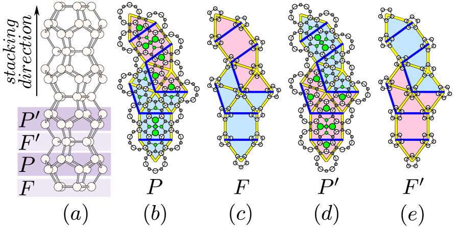
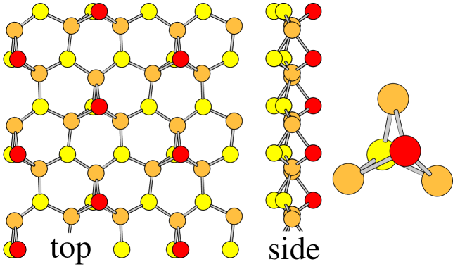
Given an R-T tiling, the backbone of the decagonal clathrate structure ( 85% of the atoms) is given just by columns of dodecahedral cages centered around tiling vertices, as illustrated in Fig. 6(a). The dodecahedra forming the column are stacked on the top of each other, defining vertical stacking period of 1.251 nm, where is the shorter face-to-face diameter of the dodecahedron. The columns possess local 10–fold screw symmetry axes , and the nearby columns related by translation over –type edges are mutually rotated by 2, implementing the bipartitness property.
The dodecahedron columns can be also viewed as stackings of “puckered” 10–rings and “flat” pentagons. Figs. 6(b-e) illustrate how this column decomposition invokes layering of the structure: the 10–rings give rise to strongly puckered –type layers, while pentagons are always located at singular height in “flat” –type layers. Full stacking period then reads , where the primed layer (10–rings or pentagons) are related to the non-primed motifs by action of the local screw axis associated with every vertex column: 2–rotation combined with half–period translation. The four stacking–period layers are centered at fractional heights = 0 (), 1/4 (), 1/2 (), and 3/4 (), respectively. While –type layers occur at single discrete heights, the –type layers span significant width of 3.2 Å, measured from the top most to the bottom most –layer atom. Separation from a topmost –layer atom to the –layer plane is 1.5 Å.
The “decoration rule” is completed by placing “interstitial” atoms outside the dodecahedral columns; these are shown as green filled circles in the Fig. 6(b-e). Upon placing the interstitial atoms, every Sn atom in the structure satisfies -bonding constraints: the coordination is strictly four, and the bond-angles vary within 105-120∘ (compared to 109.5∘ bond angles in the -Sn diamond structure).
The symmetry relationships between local atomic motifs are conveniently represented by tile coloring: both R and T tiles are either pink, or light-blue, depending on the orientation of pentagons in the and layers. / layer projected atomic positions are the same for either tile coloring, but their vertical displacements from the or fractional heights [reflected by circle sizes in Fig. 6(b-e)] are opposite for the pair of colored tiles.
| triangle (T) | rectangle (R) | |||
| Nat | 5/2 | 6 | 5 | 15 |
| [MLα] | 0.4507 | 1.0816 | 0.3646 | 1.0938 |
Table 1 summarizes the atomic content of the R and T tiles. In case of decagonal tiling, number frequency ratio of the T to R tiles is 4, and the respective tile areas are and ; hence coverage contribution in the decagonal structure will be 0.427 MLα for –type, and 1.085 MLα for –type layers.
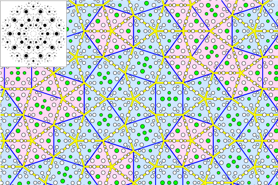
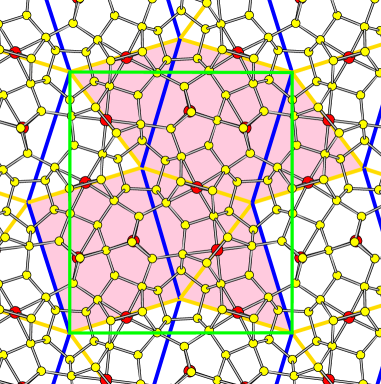
In their pure forms, the decorated R and T tilings exactly correspond to the well known canonical clathrates composed from four canonical cages, entirely filling the space. In particular, the pseudo–10-fold axis is parallel to the cubic (110) direction in clathrate Type II structure revealing isosceles triangles geometry, and to (100) direction in type III hexagonal clathrate showing pure-R tiling. Fig. 7 shows a large decagonal clathrate “approximant” with 10.25 nm 8.72 nm 1.25 nm sides of the periodic cell, in which R and T tiles pack together to form eventually large pentagonal motifs. Inset in the upper left corner of the panel shows (pseudo)-10–fold zeroth-layer of the diffraction pattern – deviation from perfect decagonal symmetry is hardly visible.
III.3.2 Decagonal clathrate – surface terminations:
We require that a proper Sn clathrate termination – in analogy with -Sn diamond surfaces – leads to at most one unsaturated bond for any atom exposed on the surface, i.e. the coordination number is . Optimization strategy based on this assumption proved successful in predicting clathrate structures of reconstructed, free-standing ultra-thin slabs as a ground–state between 2.5-7 MLα thickness for Si and Ge, and for 5–8 MLα thick Sn slabs [80]. Here, we define “thickness” or coverage in units of (111)-type monolayer of the diamond structure (-Sn in case of tin). Note that our experimental film thickness is derived from the height coordinate, hence it is not directly connected with MLα units used in this section.
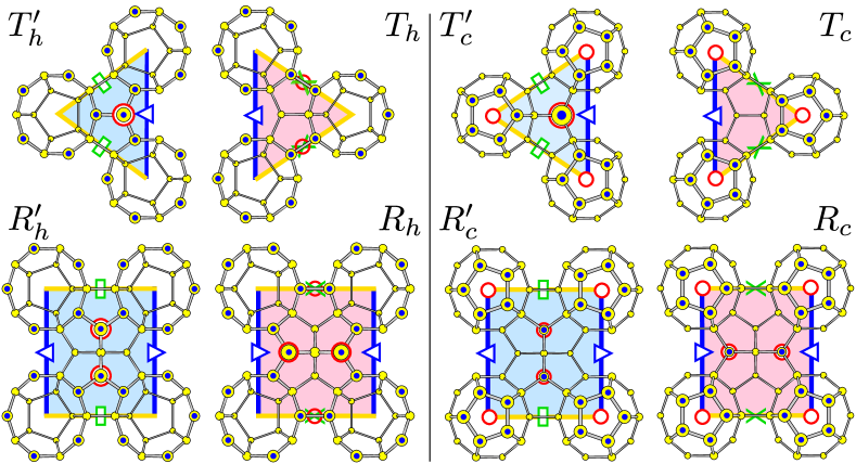
It turns out that straight planar cuts normal to the stacking direction are valid surface terminations, satisfying the coordination-number requirement, for cuts at heights in between layers defined in Fig. 6. Atoms exposed to the surface are always from two topmost layers, or or in short or layers. Termination by or bilayers with / on the top exhibits 10–rings centered on the stacked dodecahedra column axis – at the tiling vertices. Termination by or bilayer (with topmost layer) places pentagonal caps on the top of the 10–rings, thus closing the dodecahedral cages at the surface.
Fig. 8 depicts the two possible terminating surfaces for each kind of the tile on the surface: T or R tiles with topmost layer are designated / and /, respectively for the two flavors of each tile. Atoms represented by yellow circles with a blue circular spot at the center are 3–coordinated atoms that possess one unsaturated bond, each. The edge markings (green crosses/ rectangles for yellow -type linkages, blue triangles for -type linkages) implement tile packing rules for valid clathrate decorations.
Comparison with diamond structure (111)-type termination and clathrate growth: The unreconstructed (111)-type diamond surface of Sn shows puckered even–odd honeycomb lattice with even/odd sites located at two nearby planes, that are 1 Å apart from each other. The topmost sublayer exposes 3–coordinated atoms while bottom sublayer atoms are 4–coordinated. Hence, 50% of the atoms on the surface have unsaturated bonds.
In case of clathrate Sn, or terminating layers provide 1.09 MLα coverage (where MLα refers to diamond-111 surface layer), out of which 0.53 MLα atoms are 3–coordinated, the fraction 0.53/1.090.486 is very similar to the diamond structure. However, capping the 10–rings by 5-caps in another growth stage adds another 0.43 MLα coverage, while keeping the number of 3–coordinated atoms constant. Thus the (or ) bilayers terminated by 5-caps of the –type layers add 1.52 (1.09+ 0.43) MLα of the coverage, out of which less than 35% of atoms have unsaturated bonds – appreciably less than in the case of diamond. Width of one such bilayer is 6 Å, about the same as two (111)-layers of the diamond structure.
Since the 10-ring centers are laterally separated by or linkages (1-1.2 nm) shown as yellow or blue tile edges in Fig. 6, capping the 10–rings by 5-caps proceeds independently from one column of dodecahedra to another, which presumably precludes “layer-by-layer” growth mode. This is not surprising because of the 3D character of the clathrate fundamental units - cages. On the other hand, cages can be viewed as a local, relatively stable unit in which Sn atoms are not less than 3–coordinated even when the cage is entirely isolated. The unsaturated bonds on the cage surface then act effectively as attractive potential, coalescing the cages together while saturating the bonds, and minimizing the surface area during growth. We expect that the growth mode of the Sn clathrate will be either pure island or mixed island–layer type, depending on the energy scales related to processes of (1) completion of a surface cage and (2) coalescing cages together.
To summarize, in our idealized model the clathrate growth proceeds in two stages: building mutually interconnected network of the layer atoms exhibiting nearly equal number of unsaturated bonds per surface atom as the diamond structure (111)-surface, while in the second stage the 10–rings are covered by 5-caps in a stochastic process proceeding randomly/independently at any location on the surface.
III.3.3 Surface reconstruction
Terminations of -bonded surfaces necessarily produce unsaturated dangling bonds with significant energetic cost; the latter can be reduced by appropriately positioned “adatoms” that do not occupy generic lattice positions. In this subsection, we explore adatomic modifications of the clathrate surface structure by minimizing DFT surface energies.
As an example, let us first consider (111)-type surface termination of the related -bonded -Sn diamond structure, illustrated in Fig. 9 on the example of so called -reconstruction. The unreconstructed surface (i.e., without the red colored adatoms) is built up from 3–coordinated orange-colored Sn atoms in the upper half-layer of the honeycomb lattice, while the yellow 4–coordinated Sn atoms appear Å below. The yellow/orange coloring divides the underlying honeycomb lattice into even/odd parts. Its surface energy decreases from 41 to 33 meV/Å2 after positioning the Sn “adatoms” above some of the 4–coordinated atoms – they are shown in red color in Fig. 9, and the “top” view is slightly off the surface normal to make the yellow atoms visible. The placement of adatoms leads to formation of 5–atom dumbbell motifs enlarged in the rightmost panel of the figure. The remarkable aspect of this scenario is that the adatom (red in the figure) forms lateral, 2.9 Å long bonds with three nearby 3–coordinated orange Sn atoms, while being positioned 3.4 Å above the 4–coordinated yellow atom, leading to three 60∘ bond–angles between the orange–red and orange–yellow Sn atom bonds. Apparently, the advantage of saturating the lateral bonds exceeds the disadvantage from introducing the 60∘ bond–angles.
Clathrate surfaces do not offer any exactly analogous configurations of the 3–coordinated atoms on the surface. Since majority of the facets bounding the clathrate cages appearing on the surface are pentagons, the lattice of the surface clathrate atoms is not bipartite and energy optimization requires systematic search over the catalog of adatomic candidate sites. Our DFT–optimized catalog of added reconstruction sites is shown in Fig. 8, with site’s projected positions indicated by red open circles. These sites always reside about 3.4 Å below a 3–coordinated atom protruding outward from the surface layer, and they fall into four classes:
1. below the center of protruding pentagonal cap, for all -subscripted T and R tiles. The sites appear inside the closed dodecahedron cage at the surface;
2. near the center of the primed T tiles. These sites occur inside largest, 28–atom cage, and in the case of T triangle that has three nearby 3–coordinated neighbors, they are most reminiscent of the diamond-structure surface dumbbell configuration;
3. pairs of sites inside the R tiles;
4. “mid–edge” sites in Rh and Th
The surface energy calculation formally attributes increased energy relative to the bulk to the area of the open surface:
| (1) |
where is energy per periodic cell, is the number of atoms within the cell, is the energy per atom of the bulk structure, and is the surface area of the cell.
However, surface energies of the tile terminations in Fig. 8 cannot be computed directly, since even pure tilings of R or T tiles necessarily combine at least two types of the tiles – while the sample gives us single energy. Also, in order to weaken bias from having just one particular way of joining tiles together, more alternative tile-tile arrangements are necessary. In Table 2, we report surface energies (defined by Eq. 1) of eight pure decagonal tiles (shown in Fig. 8), resulting from least-squares fit according to Eq. 2 for a collection of 15 slab samples labeled by :
| 23.1 | 23.3 | 22.4 | 22.5 | 23.3 | 22.2 | 26.4 | 25.9 |
| (2) |
where is the surface energy of -th tile combination, is the fraction of -th sample surface occupied by -th pure tile. More precisely is the count of tile in sample , its area ’s are either for R tile or for T-tile (see subsection III.3.1 for definition); and are the eight fitted parameters – tile surface energies. The samples are based on three independent tilings, pure R, pure T, and R2T4. The terminations based on the latter tilings are discussed in detail below. Unit cells of the pure tilings must include pairs of tiles (see edge-matching rules in Fig. 8): RRα or TTα, where stands for “” or “” vertex-column terminations. Bulk energies entering Eq. 1 are 28.8, 45.6 and 42.9 meV/atom for T, R and R2T4 tilings respectively, relative to bulk energy of -Sn (for comparison, in our DFT setup tetragonal -Sn is 45.7 meV/atom). The samples – slabs and bulk – were relaxed until forces did not exceed 0.05 eV/Å. The “measured” surface energies ranged between 22-25.5 meV/Å2. The fitted surface energies are nearly similar around 23 meV/Å2, with the exception of T and R with 26 meV/Å2. The standard deviation is 0.4 meV/Å2, and maximal data-fit discrepancy is 0.65 in the same units. The range of the surface energies is comparable to that of hexagonal -Sn surfaces reported in Table II of Ref. [81]: 21–28 meV/Å2, and appreciably less than the -Sn (111)-type surface in ()–type adatomic reconstruction (33 meV/Å2).
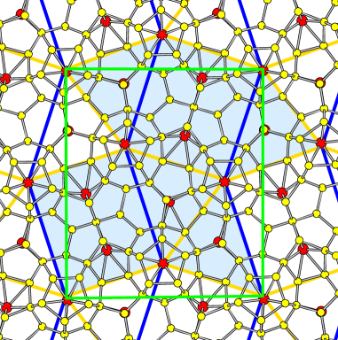
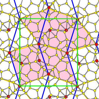
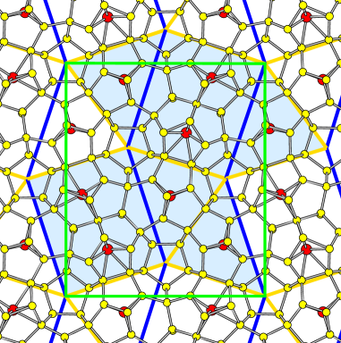
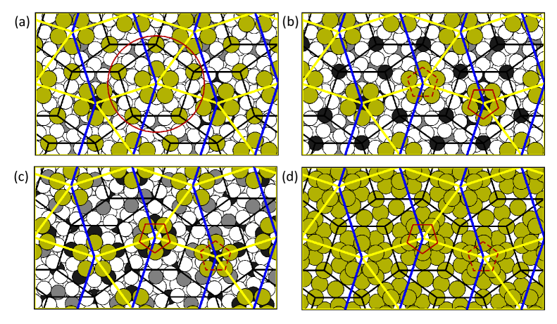
The relaxed configurations of all possible surface terminations of the R2T4 approximant mixing together R and T tiles are shown in Figs. 10 and 11. The bulk R2T4 structure is shown in Fig. S8 of SM [67] (VASP CONTCAR file is included in the SM named as “CONTCAR1” [67]). It has a space group (#55) with 148 atoms in the unit cell. The optimized lattice parameters are = 2.398 nm, = 2.055 nm and = 1.244 nm, being the stacking direction. The surface terminations as defined in Fig. 8 combine two properties: “penta-cap” or “hole” termination of the vertex column of dodecahedra, and primed/non-primed tile flavor (pink/light blue colors). From the edge-marking rules (green symbols in Fig. 8), all surface tiles in R2T4 tiling must have the same coloring – this is a non-generic property of a small periodic approximant – see representative example of large tiling from Fig. 7 in which pink/blueish tiles mix in a single layer. This leaves us with four terminations, that we implemented in three slab structures: both “penta-cap” terminations in Fig. 10 are bottom and top surface of the same 262-atom slab (made of 4+3 type layers). The primed “penta-hole” termination occurring on both surfaces of a 292–atom slab symmetrically, are made of 3+4 type layers (Fig. 11 left, blue tiling), and finally the non-primed “penta-hole” reconstruction terminates a thinner (2+3, 220 atoms) slab structure (Fig. 11 right, pink tiling). It may be noted that each of the four surfaces of the R2T4 approximant in Figs. 10,11 can be combined with numerical results from Table II following R/T labels given in the figure captions: the surface in Fig. 10 (left) has = 26 meV/Å2, and all of the three other surfaces have = 22-23 meV/Å2.
Our final remark is that the R2T4 tiling nearly exactly matches the lattice parameters and atomic motifs in W-Al-Ni-Co approximant, serving as an important hint for nucleation of the decagonal clathrate on -Al-Ni-Co, as discussed in the subsection III.4. Combining for R and T tiles from Table 1 with R2T4 tile counts and areas, we obtain coverings of 0.4 MLα for type layer and 1.09 for type layer. Fig. 12(b) shows that the initial stage of the decagonal clathrate formation is type layer.
III.4 Nucleation of Sn on -Al-Ni-Co
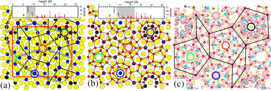
Here, we focus on the question of how the decagonal Sn clathrate nucleates on the 10f -Al-Ni-Co surface. As mentioned earlier, the bulk structure of -Al-Ni-Co has been described by a decagonal W-Al-Ni-Co approximant phase that can be cleaved at the flat A surface or at the puckered B surface [55, 54]. So, it can be expected that the local arrangement of atoms on the -Al-Ni-Co surface is similar to that in W-Al-Ni-Co. We discuss henceforth the nucleation sites of Sn on W-Al-Ni-Co, and how that is compatible with formation of the Sn clathrate layer. The arrangement of Ni and Co i.e. the transition metal (TM) atoms on the B-surface of W-Al-Ni-Co [see Fig. 1(b) of Ref. 55] can be described by the P1 tiling. On the Al-Ni-Co surface, the adsorbed Sn atoms prefer to bind with the TM atoms. The preferential adsorption of Sn atoms around surface TM atoms with formation of Sn white flowers (SnWFs) at the early stages of the Sn deposition has been observed on -Al-Pd-Mn [50].
On the B surface, there are two kinds of the preferred adsorption sites for Sn atoms. The first one is similar as that on the -Al-Pd-Mn surface. The Sn atoms can be adsorbed around the TM atom centering a pentagon of Al atoms. The second kind is a small pentagon of TM atoms, where the Sn atoms are adsorbed in their bridge positions, compared to the clean B surface [see Fig. 1(b) of Ref. 55]. Sn atoms can be adsorbed in the vertices of the P1 tiling and together with the small Sn pentagon in the center they could create the SnWF configuration [Fig. 12(a)], which is similar as on the -Al-Pd-Mn surface. On the other hand, Fig. 12(b) shows that on the B-surface, small Sn pentagons can be adsorbed at the centers of the pentagons of the P1 tiling (black lines). These pentagons can play the role of nucleation centers for growth of the Sn clathrate layer. The pentagon of Sn atoms can be adsorbed also in bridge positions of small Al pentagons (e.g., in the center of the figure) but such adsorption site is not preferred and not so stable as at the TM atoms.
If the surface in the center of the P1 pentagon is occupied by a slightly protruding Co atom [right in Fig. 12(b)], the small Sn5 cluster (traced by red down pentagon) formed around this central atom is stable. The calculated average binding energy () of Sn adatoms is (Sn5)= -0.501 eV/atom. If the center of the P1 pentagon is occupied by Al atoms [in the center of Fig. 12(b)] the position of the Sn5 adatoms (traced by dashed red up pentagon) is metastable with (Sn5)= -0.277 eV/atom. However, it was observed that in this case the outer Sn atoms, which occupy the vertices of the P1 pentagons [marked by a red circle in Fig. 12(a)] can significantly stabilize the central Sn5 cluster. Binding of outer 5 Sn atoms with the central Sn5 cluster forms the white flower (WF) configuration of 10 atoms (known also as the starfish cluster [82]). The WF configurations are frequently observed at deposition of adatoms on quasicrystalline surfaces [82, 83, 84]. The calculated binding energy of the WF cluster around the metastable Sn5 is (Sn10)= -0.396 eV/atom. The WF cluster around the most stable Sn5 cluster [right in Fig. 12(b)] reduces the average binding energy, to (Sn10)= -0.426 eV/atom. The WF configurations help to create the Sn5 clusters in the centers of the P1 tiles and can thus support the nucleation and further growth of the clathrate structure.
On the A surface of W-Al-Ni-Co, the R-T tiling can also describe ordering of atoms on a larger scale but the local arrangement of atoms inside the tiles is less regular. Although the description of arrangement of the TM atoms on the A surface is described by its own tiling, and for the current discussion it is better to put on the A surface together with the R-T tiling also the same P1 tiling as on the B surface. On the A surface, there is a higher content of TM atoms compared to the B surface. Similarly as on the B surface, they can form small TM pentagons (e.g. in the center of the figure) [Fig. 12(c)]. These small TM pentagons can be preferred adsorption centers for the Sn atoms adsorbed in the bridge positions between the TM atoms. Fig. 12(c) shows the A surface with the Sn pentagons in vertices of the R-T tiling. Similarly as on the B surface, these can be the possible nucleation centers for growth of the clathrate layer on the A surface. However, on this surface there are also additional TM atoms (inside the thin rhombi of P1) which can disturb the presented regular ordering of the Sn nucleation centers.
Fig. 12(d) shows the Sn clathrate layer that is described by the R-T tiling model (thick blue and yellow lines). The orientation of the Sn pentagons alternate with the number of the Sn clathrate layers. The present one is for one or odd number of layers. Further, on the B surface of the W-phase, the length of the Penrose P1 tiling is (P1)= 0.758 nm [55]. From this it follows that the lengths of the blue and yellow edges of the R-T tiling [Fig. 12] are (blue)= (P1)= 1.227 and (yellow)= (blue)/[2 sin(/5)]= 0.851 (blue)= 1.043 nm, respectively. The length of edges of the R-T tiling on the -Al-Ni-Co surface is thus 2.1% smaller compared to the -Al-Pd-Mn surface [50], indicating that they are almost the same. The sizes of the R-T tilings on the W-phase and -Al-Ni-Co is likely to be within 1-2%. It is remarkable that the lengths of the R-T edges for W-Al-Ni-Co surface ((yellow)= 1.043 nm and (blue)= 1.227 nm) are so close to those of the decagonal Sn clathrate obtained from DFT in subsection III.3.1 (= 1.082 nm and = 1.268 nm), see also Ref. 85.
To check the compatibility of the SnWF and the pentagon with the clathrate structure, it is important to compare the configuration of Sn adatoms forming the SnWF cluster and the pentagon on the A and B surface of W-Al-Ni-Co [Figs. 12(a-c)] with the structure of the clathrate layer [Fig. 12(d)]. The clathrate structure consists of regular dodecahedral cages of Sn atoms. The dodecahedra are centered at the vertices of the rectangular-triangular (R-T) tiling. It is clear from Fig. 12 that SnWF and the pentagons are the integral parts of the clathrate surface.
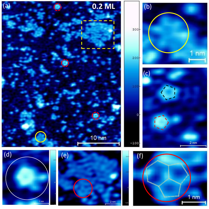
In order to experimentally probe the nucleation of the Sn clathrate on -Al-Ni-Co, we have performed STM after 0.2 ML Sn deposition (Fig. 13). A large part of the image is dispersed with isolated Sn atoms that have an atomic height of 0.170.02 nm after averaging over 110 height profiles over different Sn adatoms. However, in some regions nucleation of Sn pentagons is clearly observed as highlighted by dashed red circles in Fig. 13(a). The average diameter of the dashed red circles that enclose these pentagons is 1.50.1 nm. Furthermore, a SnWF of about 2 nm diameter [yellow circle in Figs. 13(a,b)] is also observed, as discussed above for the W-Al-Ni-Co B surface [red circle in Fig. 12(a)]. In Fig. 13(c), two pentagons that are 36∘ rotated with respect to each other are traced by dashed red and black pentagons, respectively. It may be noted that such rotated pentagonal motifs are also expected from our nucleation model discussed above for both B and A surfaces [dashed and solid red pentagons in Figs. 12(b,c)]. Fig. 13(d) shows how a pentagonal motif converts to a SnWF with Sn atoms bonding at its vertices. A region where Sn motifs coalesce to form an island [dashed yellow rectangle in Fig. 13(a)] is shown in an expanded scale in Fig. 13(e). Here, motif (red circle) formed by two pentagons and a hexagon is visible, shown zoomed Fig. 13(f). This, named as triplet motif, is compared with and shown to be a valid part of both penta-cap and penta-hole terminations of the R2T4 approximant in Fig. 15. Thus, the indication of formation of the clathrate structure is obtained even from small Sn islands at initial stage of the growth.
III.5 R2T4 approximant model of the Sn film on Al-Ni-Co substrate
W-phase approximant model structure [54] with its 530 atoms/cell utilized as a model substrate for nucleation in subsection III.3, strains the resources when the computationally intensive ab-initio approach is needed. At the same time, the W-phase periodic cell is double superstructure of the R2T4 approximant cell (the horizontal axis of the W-phase periodic cell in Fig. 12 is doubled along the horizontal axis relative to the R2T4 cell in Figs. 10, 11). So, possibly a hypothetical R2T4 Al-Ni-Co approximant preserves equally fair relationship with the -phase while requiring only 10% of the resources needed to study composite Sn/Al-Ni-Co slab within our DFT setup. The R2T4 Al-Ni-Co should not be confused with the R2T4 clathrate approximant because although they share the tiling geometry, the atomic motifs behind this coincidence are very different.
We carried out tempering simulations for the Al-Ni-Co system in the R2T4 cell in the spirit of the Al-Cu-Fe simulated annealing leading to spontaneous formation of icosahedral quasicrystal [86], using DFT-fitted empirical oscillating potentials (EOP) [87] for Al-Ni-Co. Fig. 14(a) displays -Al-Ni-Co bilayer at the –type surface analogous to its W-phase counterpart in Fig. 12(b). Details of the preparation of the R2T4-Al-Ni-Co model are gathered as a note in the SM [67], and the final DFT-relaxed structure is provided in the SM as “CONTCAR2”[67].
Although atomic structure of -Al-Ni-Co and Sn clathrate obey completely different electronic and coordination rules, their interface is perfectly coherent following the R-T tiling geometry, as indicated in Fig. 12. This allows for a straightforward approach to the Sn/Al-Ni-Co approximant composite model construction: we merge a 3–layer thick Al-Ni-Co slab (two Al–rich “puckered” layers with “flat” pseudo-mirror layer in between) with a five–layer 1.2 nm thick Sn slab (three F–type and two P–type layers). The slabs were positioned within plausible distance from each other, with shortest initial pair distances of 0.27 nm between Sn and Al/Co/Ni atoms. The open-surface side of the Sn slab was reconstructed following the primed-penta-cap recipe illustrated in Fig. 10 left, and 1.2 nm thick vacuum slab was inserted between the Sn surface and the “bottom” of the periodic image of Al-Ni-Co slab. The resulting composite slab had Sn180/Al150Co32Ni18 content in the = 2.34 nm, = 1.98 nm and = 3.09 nm orthorhombic cell (the axis is parallel to the pseudo-10-fold axis), and its “bottom” –layers relaxed structure is presented in Fig. 14(b). The final optimized structure can be found in “CONTCAR3” [67].
The structural relaxation was executed under our DFT setup, using 4 and finally 16 -points mesh, but with the rectangular cell fixed at bulk Al-Ni-Co- optimal size. During the relaxation, the structure settled quickly into a local minimum with negligible residual forces and rather small -3 kBar pressure. In order to estimate strength of the binding between Sn/Al-Ni-Co slabs, we separated Sn and Al-Ni-Co sub–slabs by another 1.2 nm –wide vacuum gap, and re-relaxed the structure (holding the cell fixed). We find the “work of separation” (or adhesion) defined as 60.4 meV/Å2 (area and between composite slab and vacuum–separated Sn and Al-Ni-Co slabs in eV per cell) to be nearly identical to the 64.4 meV/Å2 of the pure clathrate II structure normal to its 3–fold cubic direction. This shows that the strength of the attachment between the Sn-clathrate film and the Al-Ni-Co substrate is close to the self- separation of the clathrate itself.
The gross picture offered by charge–density isosurface taken at =0.02 ( denotes the valence electron density) and displayed in Fig. 14(c) (slice widths as in panel b) is as follows: the charge mainly accumulates around transition metal (TM) atoms (that are hidden inside the isosurfaces), with lobes of the surfaces pointing toward the Al or Sn atoms, and indicating a charge-transfer from the Al/Sn atoms. Second, with the exception of the “bottom”–most Sn atoms, characteristic dumbbell-like charge pockets accumulate around the Sn–Sn bond mid-points, indicating clear character of these electronic states. Side–view of the isosurfaces (not shown) reveals that the crucial interface bonding occurs via strong covalent 0.27 nm bonds normal to the interface between Sn and Co atoms, located at the vertices of the tiling (black lines in the panel (c)): these are the well-known –cluster tips introduced in the previous section.
To summarize, DFT study of the Sn/Al-Ni-Co interface based on the tiling geometry confirms that (i) there are essentially two types of Sn atoms in the first ML: isolated Sn at the vertices of the tiling above Co atoms bonding to them by strong covalent bonds; and Sn-pentagons at the vertices of the R-T tiling, occurring above several distinct pentagonal Al-Ni-Co motifs, supporting the findings of the previous section; (ii) above this first ML, Sn builds up stable -bonded clathrate structure.
III.6 Motifs from STM compared to the relaxed R2T4 structural model
In this section, we define the different types of motifs, each highlighted by similar line-type in the STM images in Figs. 1, 3, 4 and 13) based on the energy-optimized relaxed surface of the R2T4 clathrate approximant in Fig. 15. Thereafter, a comparison is provided between STM and theory in Figs. 16, 17.
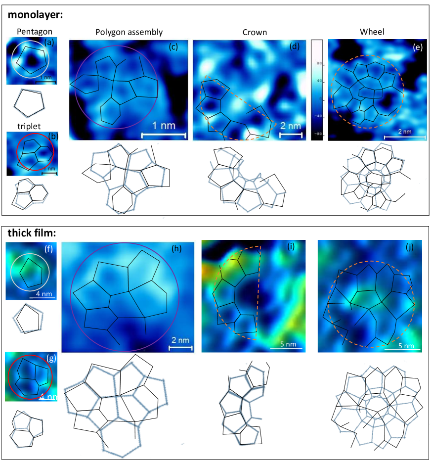
The wheel motif enclosed by dashed orange circle in Fig. 15 is a nearly decagonal congregation of 10 polygons (8 pentagons and two hexagons) with common sides. Sn atoms decorate their vertices. Incomplete wheels with more than 5 polygons are also referred to as the wheel motif. Also note that the polygons are not regular, the length of their sides have a mean value of 0.3 nm with standard deviation of 0.01 nm [Fig. 15]. A perfectly decagonal wheel with ten pentagons does not occur in the R2T4 approximant, but this is a feasible object if a bigger approximant is considered. It simply corresponds to a particular tiling pattern, namely five triangles forming pentagons with blue tiling edges. The wheel motifs are found on both the “penta-cap” and “penta-hole” surfaces, as shown in Fig. 15(a,b), respectively. In the former, the decagon is capped with the possible occurrence of adatom, which would give a bright contrast at the center in the STM image. In the latter, the decagon is not capped, resulting in a relatively darker center of the wheel motif. The crown motif is a part of the wheel motif comprising of 5 polygons highlighted by a dashed orange half-circle in Fig. 15. The polygon assembly with variable number of polygons comprises of the overlapping regions of two adjacent wheel motifs and consist of pentagons with/without a hexagon (violet circles). The triplet motif is a smaller version of the polygon assembly, comprising of two pentagons and one hexagon (red circles). The pentagon motif has its vertices decorated by the five top most Sn atoms in the center region of the “penta-cap” wheel , as shown by a gray circle in Fig. 15(a).
The above defined motifs are compared with the STM images in Fig. 16 for two different thicknesses. It is interesting to observe that there is an inflation between the motifs of the monolayer [Fig. 16(a-e)] and the 10 nm film [Fig. 16(f-j)], which is estimated to be ∼. For example, the average diameter of the wheel motif is 4.50.5 nm for monolayer, 8.81 nm for 0.9 nm and 14.51 nm for the 10 nm film. This shows inflation by a factor of 3.20.4 between monolayer and the 10 nm film, which is close to (= 3.08). Similarly, inflation by a factor of 1.650.2 between the 0.9 nm and the 10 nm film is close to (= 1.618). This is consistent with the finding that the theoretical model requires an inflation of for good agreement with the sizes the monolayer motifs, whereas it is for the 0.9 nm film and for the 10 nm film.
Inflation is a well known property of the quasiperiodic systems due to their self-similar nature and has been observed in both ternary and binary quasicrystals [91, 92, 90, 89, 50]. A well-known example is -Al-Pd-Mn, where the fundamental inter cluster linkage of 7.75 Å is () inflated along the twofold (fivefold) direction. inflation has also been reported in a binary quasicrystal Yb-Cd with the formation of a cluster of clusters [90]. Inflation could be caused with respect to the theoretical model by the formation of self-similar structures with the inclusion of extra atoms such that the local bonding characteristics remain similar. In our previous work, we showed that the STM image from 3-4 nm thick Sn film on -Al-Pd-Mn shows inflation with respect to the theoretical clathrate model [50]. Here, from Fig. 16, we find satisfactory agreement in the sizes of the STM motifs and the R2T4 model at a fixed inflated length scale for all the motifs at a particular thickness. This is an indication of the propagation of quasiperiodic ordering in the film.
The pentagon motif in Figs. 16(a,f) is the smallest of all the motifs and is traced by black lines that join the bright vertices. It is also the most abundantly observed motif, for example, see Fig. 4(d). The tracing of the triplet motif by black lines revealing its internal structure is shown in Figs. 16(b,g). The tracings of these motifs are juxtaposed on the R2T4 model below each image in same length scale, and the agreement is rather good for both the thicknesses vindicating the clathrate model. Note that the triplet motif is also observed for 0.2 ML Sn deposition in Fig. 13(f), and the agreement with the R2T4 model is satisfactory.
The polygon assembly motif is also observed in both the monolayer as well as the thick film, as shown in Figs. 16(c,h), respectively. The crown motif in Fig. 16(d) with bright center for the monolayer in contrast to a dark centered one in Fig. 16(g) for the 10 nm film shows existence of both “penta-cap” and “penta-hole” type surfaces. A crown motif on the 0.9 nm Sn film is shown in Fig. S6(a) of SM [67]. The wheel motifs are shown in Figs. 16(e,j), as well as in Figs. S4(b) and Fig. S6(b) of SM [67], the latter being for the 0.9 nm thickness film. When juxtaposed on the R2T4 model, the tracings of these bigger motifs (polygon assembly, crown, and wheel) reveal their size similarity after inflation. Moreover, the ratio of the sizes of the pentagon and the wheel motifs is in good agreement between STM and theoretical model. However, in contrast to smaller motifs such as the pentagon and triplet, the underlying structure of the larger motifs is only partially consistent with the clathrate model. Nevertheless, this partial agreement is also a significant result given that stochastic processes and competing disorder would have a greater influence on the bigger motifs. Moreover, the puckering and roughness of the films could also play a role. This is also revealed in the theoretical model, where the atoms deviate considerably from the - plane: Fig. 15 show that the average height of the Sn atoms is = 0.250.12 nm, where the standard deviation provides an estimate of the puckering. In the R2T4 model, two Sn atoms, for instance, forming a side of the pentagon in the wheel motif and pointing in the radial direction, are often at a greater height than the remaining three atoms. In STM, this side would look brighter, but other sides containing Sn atoms at a lower height may appear darker. Thus, the STM pictures may not depict entire and regular polygons. The comparatively modest size of the R2T4 approximant may also contribute to the discrepancy between STM and the model; the internal structure of a larger approximant may result in a better agreement.
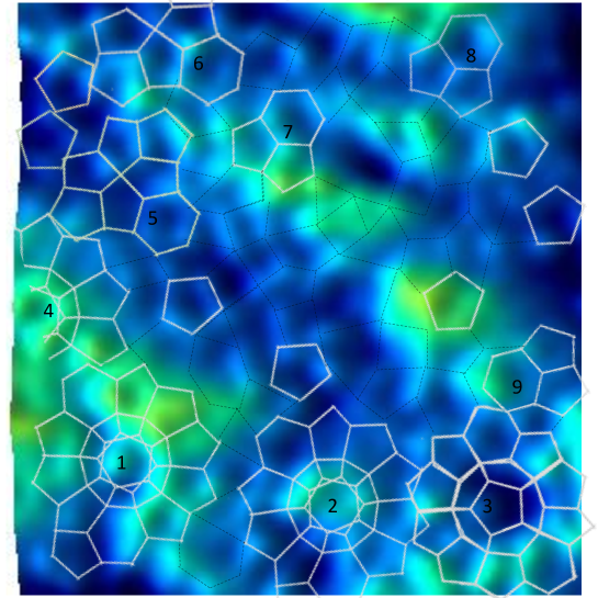
In Fig. 17, the different motifs (numbered #1- #9) of R2T4 approximant clathrate model are overlaid on (white lines) the STM image of the Sn thick film after allowing for rotation (motifs #2- #9 need to be rotated by different angles with respect to motif #1). In this way, we find that a region of 80050 nm2 is in good agreement with our model. Requirement of rotation can be related to the the formation of ring joining the spots in the LEED pattern [Fig. 5(a,b)]. The regions that do not follow the R2T4 model are traced by black dashed lines in Fig. 17. Such regions could exist because of competing disordered structures since for the thick Sn films with clathrate multilayers (that has not been calculated by DFT), the advantage of interfacial compatibility would be reduced.
Last but not least, the Sn motifs on -Al-Pd-Mn that reflect the clathrate structure [50] and those on -Al-Ni-Co exhibit a considerable degree of similarity. Figure S9 depicts this for the pentagon, triplet, crown, and wheel designs. The formation of the clathrate quasiperiodic structure on two distinct types of quasicrystalline surfaces implies that it is an inherent characteristic of Sn.
IV Conclusions
We have carried out a combined experimental and theoretical study to probe the possible occurrence of quasiperiodicity in Sn films grown on -Al-Ni-Co up to an average thickness of 10 nm. Decagonal spots in the LEED pattern, characteristic motifs and the FFT of the STM topography images establish decagonal quasiperiodicity in the Sn thin film (1 nm). For the thicker films up to the largest thickness of 10 nm where the effective potential of the substrate is negligible [88, 93], the motifs, weak LEED and FFT are also observed, showing that partial decagonal structural correlations are maintained in spite of the competing disorder. The clathrate atomic positions of the DFT-relaxed decagonal clathrate structure reveal remarkable inflation relationship with STM. The internal structure of the smaller motifs such as pentagon and triplet show good agreement with our DFT based relaxed R2T4 approximant clathrate structural model, while for the larger motifs the agreement is partial. This model is the most-likely hypothesis for the Sn structure because (i) compatibility of the clathrate structure with the substrate resulting from very similar edge lengths (within 1%) of the R-T tiling of the R2T4-approximant and the B surface of W-Al-Ni-Co approximant for the -Al-Ni-Co surface, (ii) the ground states of the thicker slabs are -bonded, the metallic Sn structures are only stabilized by vibrational entropy at elevated temperatures; (iii) the clathrate has significantly lower surface energy than the -Sn, hence for sufficiently thin films clathrate structure has lower energy, and (iv) the “work of separation” or “adhesion” of Sn/-Al-Ni-Co turns out to be comparable to the same quantity calculated for the clathrate itself proving that the clathrate Sn effectively binds to the -Al-Ni-Co surface.
V Acknowledgments
M.M. and M.K. are thankful for the support from the Slovak Grant Agency VEGA (No. 2/0144/21) and APVV (No. 15-0621, No. 19-0369). Parts of the calculations were performed in the Computing Center of the Slovak Academy of Sciences using the supercomputing infrastructure acquired under Projects ITMS 26230120002 and 26210120002. R. Batabyal is specially thanked for important suggestions and a careful reading of the manuscript. M. Balal, P. Sadhukhan, and S. Barman are thanked for support. The growth of -Al-Ni-Co single grain substrate done at Ames laboratory was supported by the U.S. Department of Energy, Office of Basic Energy Science, Division of Materials Sciences and Engineering. Ames Laboratory is operated for the U.S. Department of Energy by Iowa State University under Contract No. DE-AC02-07CH11358.
e-mail addresses: †Marek.Mihalkovic@savba.sk, ∗∗Marian.Krajci@savba.sk, #barmansr@gmail.com
References
- [1] D. Shechtman, I. Blech, D. Gratias, and J. W. Cahn, Phys. Rev. Lett. 53, 1951 (1984).
- [2] A. P. Tsai, J. Q. Guo, E. Abe, H. Takakura, and T. J. Sato, Nature (London) 408, 537 (2000).
- [3] S. Fischer, A. Exner, K. Zielske, J. Perlich, S. Deloudi, W. Steurer, P. Lindner, and S. Förster, Proc. Natl. Acad. Sci. U.S.A. 108, 1810 (2011).
- [4] D. V. Talapin, V. E. Shevchenko, I. M. Bodnarchuk, X. Ye, J. Chen, and C. B. Murray, Nature (London) 461, 964 (2009).
- [5] C. Xiao, N. Fujita, K. Miyasaka, Y. Sakamoto, and O. Terasaki, Nature (London) 487, 349 (2012).
- [6] X. Ye, J. Chen, M. E. Irrgang, M. Engel, A. Dong, S. C. Glotzer, and C. B. Murray, Nat. Mater. 16, 214 (2017).
- [7] J. D. Cain, A. Azizi, M. Conrad, S. M. Griffin, and A. Zettl, Proc. Natl. Acad. Sci. U.S.A. 117, 26135 (2020).
- [8] S. J. Ahn, P. Moon, T.-H. Kim, H.-W. Kim, H.-C. Shin, E. H. Kim, H. W. Cha, S.-J. Kahng, P. Kim, M. Koshino, Y.-W. Son, C.-W. Yang, and J. R. Ahn, Science 361, 782 (2018).
- [9] W. Yao, E. Wang, C. Bao, Y. Zhang, K. Zhang, K. Bao, C. K. Chan, C. Chen, J. Avila, M. C. Asensio, J. Zhu, and S. Zhou, Proc. Natl. Acad. Sci. U.S.A. 115, 6928 (2018).
- [10] L. Bindi, J. M. Eiler, Y. Guan, L. S. Hollister, G. MacPherson, P. J. Steinhardt, and N. Yao, Proc. Natl. Acad. Sci. U.S.A. 109, 1396 (2012).
- [11] S. S. Kang, J. M. Dubois, and J. V. Stebut, J. Mater. Res. 8, 2471 (1993).
- [12] J. M. Dubois, S. S. Kaing, and A. Perrot, Mater. Sci. Eng. A179/A180, 122 (1994).
- [13] S. J. Poon, Adv. Phys. 41, 303 (1992).
- [14] S. Sarkar, M. Krajčí, P. Sadhukhan, V. K. Singh, A. Gloskovskii, P. Mandal, V. Fournée, M. de Weerd, J. Ledieu, I. R. Fisher, and S. R. Barman, Phys. Rev. B 103, L241106 (2021).
- [15] J. Nayak, M. Maniraj, A. Rai, S. Singh, P. Rajput, A. Gloskovskii, J. Zegenhagen, D. L. Schlagel, T. A. Lograsso, K. Horn, and S. R. Barman, Phys. Rev. Lett. 109, 216403 (2012).
- [16] R. Chen, C.-Z. Chen, J.-H. Gao, B. Zho, and D.-H. Xu, Phys. Rev. Lett. 124, 036803 (2020).
- [17] J. Fan and H. Huang, Front. Phys. 17, 13203 (2022).
- [18] P. Guyot and M. Audier, C. R. Physique 15, 12 (2014).
- [19] F. C. Frank and J. S. Kasper, Acta. Crystallogr. 11, 184 (1958).
- [20] F. C. Frank and J. S. Kasper, Acta. Crystallogr. 12, 483 (1959).
- [21] D. R. Nelson and F. Spaepen, Solid State Phys. 42, 1 (1989).
- [22] J.-F. Sadoc and R. Mossieri, Geometric Frustration (Cambridge University Press, Cambridge, 1999).
- [23] D. P. Shoemaker and C. B. Shoemaker, Introduction to Quasicrystals, edited by M. V. Jaric (Academic Press, London, 1988), pp. 1–57.
- [24] V. Elser and C. L. Henley, Phys. Rev. Lett. 55, 2883 (1985).
- [25] M. Audier and P. Guyot, Philos. Mag. B 53, L43 (1986).
- [26] S. Sachdev and D. R. Nelson, Phys. Rev. B 32, 4592 (1985).
- [27] M. C. Schafer and S. Bobev, J. Am. Chem. Soc. 135, 1696 (2013).
- [28] Y. Sun, J. Lv, Y. Xie, H. Liu, and Y. Ma, Phys. Rev. Lett. 123, 097001 (2019).
- [29] H. Lin, S. Lee, L. Sun, M. Spellings, M. Engel, S. C. Glotzer, and C. A. Mirkin, Science 355, 931 (2017).
- [30] L. Zhu, G. M. Borstad, H. Liu, P. A. Guńka, M. Guerette, J.-A. Dolyniuk, Y. Meng, E. Greenberg, V. B. Prakapenka, B. L. Chaloux, A. Epshteyn, R. E. Cohen, and T. A. Strobel, Sci. Adv. 6, eaay8361 (2020).
- [31] M. S. Ikeda, H. Euchner, X. Yan, P. Tomeš, A. Prokofiev, L. Prochaska, G. Lientschnig, R. Svagera, S. Hartmann, E. Gati, M. Lang, and S. Paschen, Nat. Commun. 10, 887 (2019).
- [32] L. Zhu, T. A. Strobel, and R. E. Cohen, Phys. Rev. Lett. 125, 127601 (2020).
- [33] J. Ghosh, R. R. J. Methikkalam, R. G. Bhuin, G. Ragupathy, N. Choudhary, R. Kumar, and T. Pradeep, Proc. Natl. Acad. Sci. U.S.A. 116, 1526 (2019).
- [34] B. B. Iversen, A. E. C. Palmqvist, D. E. Cox, G. S. Nolas, G. D. Stucky, N. P. Blake, and H. Metiu, J. Solid State Chem. 149, 455 (2000).
- [35] T. Takabatake, K. Suekuni, T. Nakayama, and E. Kaneshita, Rev. Mod. Phys. 86, 669 (2014).
- [36] T. Kume, F. Ohashi, and S. Nonomura, Jpn. J. Appl. Phys. 56, 05DA05 (2017).
- [37] J.-A. Dolyniuk, B. O. -Baird, J. Wang, J. V. Zaikina, and K. Kovnir, Mater. Sci. Eng. R Rep. 108, 1 (2016).
- [38] J. Gryko, P. F. McMillan, R. F. Marzke, G. K. Ramachandran, D. Patton, S. K. Deb, and O. F. Sankey, Phys. Rev. B 62, R7707 (2000).
- [39] A. M. Guloy, R. Ramlau, Z. Tang, W. Schnelle, M. Baitinger, and Y. Grin, Nature (London) 443, 320 (2006).
- [40] S. Christensen, L. Bjerg, A. Kaltzoglou, F. Juranyi, T. Fassler, T. Unruh, and M. Christensen, J. Appl. Phys. 113, 084002 (2013).
- [41] J. Yuhara, Y. Fujii, K. Nishino, N. Isobe, M. Nakatake, L. Xian, A. Rubio, and G. L. Lay, 2D Mater. 5, 025002 (2018).
- [42] P. Sadhukhan, S. Barman, T. Roy, V. K. Singh, S. Sarkar, A. Chakrabarti, and S. R. Barman, Phys. Rev. B 100, 235404 (2019).
- [43] P. Sadhukhan, D. Pandey, V. K. Singh, S. Sarkar, A. Rai, K. Bhattacharya, A. Chakrabarti, and S. R. Barman, Appl. Surf. Sci. 506, 144606 (2020).
- [44] V. A. Rogalev, F. Reis, F. Adler, M. Bauernfeind, J. Erhardt, M. R. Scholz, L. Dudy, L. B. Duffy, T. Hesjedal, M. Hoesch, G. Bihlmayer, J. Schäfer, and R. Claessen, Phys. Rev. B 100, 245144 (2019).
- [45] M. Liao, Y. Zang, Z. Guan, H. Li, Y. Gong, K. Zhu, X.-P. Hu, D. Zhang, Y. Xu, Y.-Y. Wang, K. He, X.-C. Ma, S.-C. Zhang, and Q.-K. Xue, Nat. Phys. 14, 344 (2018).
- [46] D. D. Sante, P. Eck, M. Bauernfeind, M. Will, R. Thomale, J. Schfer, R. Claessen, and G. Sangiovanni, Phys. Rev. B 99, 0351245 (2019).
- [47] Z. Shi, X. Wang, C. Xu, P. Wang, Y. Liu, and T.-C. Chiang, Phys. Lett. A 384, 126782 (2020).
- [48] N. Si, Q. Yao, Y. Jiang, H. Li, D. Zhou, Q. Ji, H. Huang, H. Li, and T. Niu, J. Phys. Chem. Lett. 11, 1317 (2020).
- [49] Y. Xu, B. Yan, H.-J. Zhang, J. Wang, G. Xu, P. Tang, W. Duan, and S.-C. Zhang, Phys. Rev. Lett. 111, 136804 (2013).
- [50] V. K. Singh, M. Mihalkovič, M. Krajčí, S. Sarkar, P. Sadhukhan, M. Maniraj, A. Rai, K. Pussi, D. L. Schlagel, T. A. Lograsso, A. K. Shukla, and S. R. Barman, Phys. Rev. Res. 2, 013023 (2020).
- [51] A. P. Tsai, A. Inoue, and T. Masumoto, Mater. Trans., JIM 30, 463 (1989).
- [52] K. Hiraga, W. Sun, and A. Yamamoto, Mater. Trans., JIM 35, 657 (1994).
- [53] A. Yamamoto and S. Weber, Phys. Rev. Lett. 78, 23 (1997).
- [54] K. Sugiyama, S. Nishimura, and K. Hiraga, J. Alloys Compd. 342, 65 (2002).
- [55] M. Krajčí, J. Hafner, and M. Mihalkovič, Phys. Rev. B 73, 134203 (2006).
- [56] V. Fournée, A. R. Ross, T. A. Lograsso, J. W. Evans, and P. A. Thiel, Surf. Sci. 537, 5 (2003).
- [57] W. R. Tyson and W. A. Miller, Surf. Sci. 62, 267 (1977).
- [58] M. Shimoda, J. Guo, T. Sato, and A.-P. Tsai, J. Non-Cryst. Solids 334, 505 (2004).
- [59] C. A. Schneider, W. S. Rasband, and K. W. Eliceiri, Nat. Methods 9, 671, (2012).
- [60] I. R. Fisher, M. J. Kramer, Z. Islam, A. R. Ross, A. Kracher, T. Wiener, M. J. Sailer, A. I. Goldman and P. C. Canfield, Philos. Mag. B 79, 425 (1999).
- [61] P. C. Canfield, Rep. Prog. Phys. 83 016501 (2020).
- [62] V. K. Singh and S. R. Barman, AIP Conf. Proc. 2265, 030311 (2020).
- [63] A. K. Shukla, S. Banik, R. S. Dhaka, C. Biswas, S. R. Barman, and H. Haak, Rev. Sci. Instrum. 75, 4467 (2004).
- [64] G. Kresse and J. Furthmuller, Phys. Rev. B 54, 11169 (1996).
- [65] G. Kresse and D. Joubert, Phys. Rev. B 59, 1758 (1999).
- [66] J. P. Perdew, J. A. Chevary, S. H. Vosko, K. A. Jackson, M. R. Pederson, D. J. Singh, and C. Fiolhais, Phys. Rev. B 46, 6671 (1992).
- [67] See Supplemental Material for Figs. S1– S9, Tables SI-III, a note, 3 CONTCAR files, and 7 video files.
- [68] H. R. Sharma, K. J. Franke, W. Theis, A. Riemann, S. Flsch, P. Gille, and K. H. Rieder, Phys. Rev. B 70, 235409 (2004).
- [69] T. Haibach , A. Cervellino , M. A. Estermann, and W. Steurer, Phil. Mag. A 79, 933 (1999).
- [70] A. Rai, V. K. Singh, J. Nayak, and S. R. Barman, Surf. Sci. 679, 169 (2019).
- [71] K. Heinz, Rep. Prog. Phys. 58, 637 (1995).
- [72] R. D. Diehl, Th. Seyller, M. Caragiu, G. S. Leatherman, N. Ferralis, K. Pussi, P. Kaukasoina, and M. Lindroos, J. Phys.: Condens. Matter 16, S2839 (2004).
- [73] K. Pussi, N. Ferralis, M. Mihalkovič, M. Widom, S. Curtarolo, M. Gierer, C. J. Jenks, P. C. Canfield, I. R. Fisher, and R. D. Diehl, Phys. Rev. B 73, 184203 (2006).
- [74] S. Sarkar, S. Barman, M. Balal, and S. R. Barman, Appl. Surf. Sci. 563, 150067 (2021).
- [75] H. R. Sharma, J. A. Smerdon, P. J. Nugent, A. Ribeiro, I. McLeod, V. R. Dhanak, M. Shimoda, A.-P. Tsai, and R. McGrath, J. Chem. Phys. 140, 174710 (2014).
- [76] M. Engel, P. F. Damasceno, C. L. Phillips, and S. C. Glotzer, Nat. Mater. 14, 109 (2014).
- [77] J. Vuorinen, K. Pussi, R. D. Diehl, and M. Lindroos, J. Phys.: Condens. Matter 24, 015003 (2012).
- [78] M. O’Keeffe, G. B. Adams, and O. F. Sankey, Philos. Mag. Lett. 78, 21 (1998).
- [79] M. Mihalkovič, J. Richmond-Decker, C. L. Henley, and M. Oxborrow, Phil. Mag. 94, 1529 (2014).
- [80] E. Pospisilova and M. Mihalkovič, manuscript in preparation.
- [81] N. G. Hormann, A. Gross, J. Rohrer, and P. Kaghazchi, Appl. Phys. Lett. 107, 123101 (2015).
- [82] J. Ledieu, M. Krajčí, J. Hafner, L. Leung, L. H. Wearing, R. McGrath, T. A. Lograsso and D. Wu, V. Fournée, Phys. Rev. B 79, 165430, (2009).
- [83] J. A. Smerdon, J. K. Parle, L. H. Wearing, T. A. Lograsso, A. R. Ross, and R. McGrath, Phys. Rev. B 78, 075407 (2008).
- [84] M. Maniraj, A. Rai, and S. R. Barman, M. Krajčí, D. L. Schlagel, T. A. Lograsso, and K. Horn, Phys. Rev. B 90, 115407 (2014).
- [85] For W-Al-Ni-Co, the lattice parameters optimized by DFT are by factor 0.9975 shorter than the experimental lattice. The fundamental -Sn structure yields optimized lattice parameters by 1.023 factor longer than the experiment. The DFT lattice mismatch computed for the R2T4 approximants of the Sn-clathrate versus -Al-Ni-Co is 1.033. Thus, our extrapolated realistic mismatch estimate is 1.033/1.0230.9975 = 1.007.
- [86] M. Mihalkovič and M. Widom, Phys. Rev. Res. 2, 013196 (2020).
- [87] M. Mihalkovič and C. L. Henley, Phys. Rev. B 85, 092102 (2012).
- [88] L.-H. Ye, Phys. Rev. B 92, 115132 (2015).
- [89] A. E. Madison, Phys. Solid State 56, 1706 (2014).
- [90] H. Takakura, C. P. Gomez, A. Yamamoto, M. D. Boissieu, and A. P. Tsai, Nat. Mater. 6, 58 (2007).
- [91] M. Krajčí and J. Hafner, in Quasicrystals, Series in Handbook of Metal Physics, edited by T. Fujiwara and Y. Ishii (Elsevier, Amsterdam, 2008) Vol. 2, Chap. 9, pp. 313–55.
- [92] A. P. Tsai and C. Cui, in Handbook of Crystal Growth, edited by T. Nishinaga (Elsevier, Amsterdam, 2015) Chap. 26, pp. 1113–56.
- [93] N. D. Lang and W. Kohn, Phys. Rev. B 1, 4555 (1970).