Nanomechanical resonators fabricated by atomic layer deposition on suspended 2D materials
Abstract
Atomic layer deposition (ALD), a layer-by-layer controlled method to synthesize ultrathin materials, provides various merits over other techniques such as precise thickness control, large area scalability and excellent conformality. Here we demonstrate the possibility of using ALD growth on top of suspended 2D materials to fabricate nanomechanical resonators. We fabricate ALD nanomechanical resonators consisting of a graphene/MoS2 heterostructure. Using AFM indentation and optothermal drive, we measure their mechanical properties including Young’s modulus, resonance frequency and quality factor, showing similar values as their exfoliated and chemical vapor deposited counterparts. We also demonstrate the fabrication of nanomechanical resonators by exfoliating an ALD grown NbS2 layer. This study exemplifies the potential of ALD techniques to produce high-quality suspended nanomechanical membranes, providing a promising route towards high-volume fabrication of future multilayer nanodevices and nanoelectromechanical systems.
The properties of 2D materials, in particular their ultralow weight and ultrahigh mechanical flexibility, provides them with an excellent sensitivity to external forces Barton et al. (2011); Zhu et al. (2022); Lee et al. (2013). Hence, resonators from 2D materials have become a popular choice for the next generation of nanoelectromechanical systems (NEMS) Steeneken et al. (2021); Lemme et al. (2020). Recently, there is surge towards stacking different 2D materials into heterostructures often exhibiting better sensing properties. Such heterostructures are used for tunable resonators and oscillators Ye et al. (2021), and can potentially lead to better sensors in microphone and pressure sensing applications Lemme et al. (2020).
To achieve high-performance nanomechanical resonators, clean interfaces between different 2D materials are important Mackus, Bol, and Kessels (2014). Therefore, bottom-up synthesis methods were developed, of which chemical vapor deposition (CVD) is the most attractive due to its large-scale and high-quality growth. The main shortcoming of CVD, however, is the difficulty to accurately control the thickness and morphology of grown 2D materials. Atomic layer deposition (ALD), a vapor phase thin film deposition technique based on self-limiting surface reactions, inherently yields atomic-scale thickness control, excellent uniformity, and conformality Sharma et al. (2018). ALD processes exists for a large variety of materials ranging from pure elements to metal oxides and chalcogenides Vos et al. (2016). In terms of 2D materials, ALD was applied to fabricate 2D-based field effect transistors, p-n diode devices, solar cells and photodetectors, displaying high electrical and optical uniformities Hao, Marichy, and Journet (2018). Since layer thickness control is essential for realizing uniform mechanical properties, it is of interest to explore the potential of ALD materials for nanomechancial resonators.
In this letter, we show two types of nanomechancial resonators fabricated using ALD: one consists of a heterostructure made from exfoliated graphene (bottom layer) and ALD MoS2 (top layer) and the other is ALD NbS2. We use atomic force microscope (AFM) indentation to determine their Young’s moduli and use an optomechanical method to study their resonance frequency and corresponding quality factor in vacuum conditions. The extracted parameters from our measurements agree well with literature values for 2D exfoliated or CVD resonators. Furthermore, by fitting a relation between the quality factors before and after ALD, we verify a low-level dissipation induced by ALD MoS2. Our work indicates the potential of ALD fabrication techniques for realizing multilayer nanomechanical membranes and resonators with enhanced functionality and thickness control.
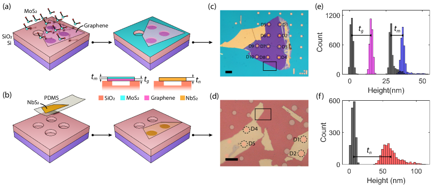
The ALD layers are deposited (see Figs. 1a and b) by plasma-enhanced atomic layer deposition (PE-ALD) technique using an Oxford Instruments Plasma Technology FlexAL ALD reactor. The base pressure of the system is 10-6 . The metal-organic precursors bis(tert-butylimido)-bis(dimethylamido) molybdenum (STREM Chemical, Inc., 98) and (tert-butylimido)-tris-(diethylamino)-niobium (STREM Chemical, Inc., 98) are used for MoOx and NbOx growth, respectively Vos et al. (2016); Basuvalingam et al. (2018). The Mo and Nb precursors are kept in stainless steel bubblers at 50 and 65 , respectively and are bubbled using Ar as the carrier gas. In both the processes, O2 plasma is used as the coreactant. The MoOx and NbOx films are deposited at 100 and 150 , respectively.
Both the MoS2 and NbS2 films are synthesized by a two step approach. As the first step, metal oxide (MoOx or NbOx) film is deposited by PE-ALD technique. Next, the metal oxide film is sulfurized at 900 in H2S environment (10 H2S and 90 Ar) to form metal sulfide film (MoS2 or NbS2). As shown in Figs. 1a and 1c, the MoS2 film is synthesized by PE-ALD on top of suspended graphene drums, resulting in 10 resonators with a radius . Note that device D3 and D9 broke (buckled, Fig. 1c) during fabrication and will not be considered further. On the other hand, NbS2 film is synthesized by growing NbOx on glassy carbon followed by sulfurization at 900 . Then, we fabricate the NbS2 resonators by transferring the NbS2 films from glassy carbon substrate over circular cavities in a SiO2/Si substrate to form suspended drums using the Scotch tape method Lemme et al. (2020) (see Fig. 1b). The cavities have a depth of and were fabricated by reactive ion etching Steeneken et al. (2021). The fabricated NbS2 resonators, shown in Fig. 1d, have a radius of (devices D1 and D2) or (devices D4 and D5). We use AFM (tapping mode) to scan the surface of our fabricated samples, to determine the thickness of the 2D materials. By calculating the height difference between the membranes and substrate (see the statistics in Figs. 1e and 1f), we extract the mean thickness of the graphene (40 layers), MoS2 (13 layers) and NbS2 (92 layers), respectively. The total thickness of the heterostructure is thus .
After fabrication, we determine the Young’s modulus of the ALD devices by indenting with an AFM (contact mode) cantilever at the centre of the suspended area (see Fig. 2a, insert). Following literature Castellanos-Gomez et al. (2012), the applied vertical force versus membrane deflection for a circular membrane (composed of single material), as depicted in Fig. 2a, is given by
| (1) |
where is bending rigidity, is Young’s modulus, is the Poisson ratio, is pretension, , and is a factor that quantifies the effect of interlayer shear interactions on in multilayer 2D materials Wang et al. (2019). The first two terms in Eq. 1 scale linearly with () and are set by and ; while the third cubic term () is due to the geometric nonlinearity of the membrane, which lead to an increase in the in-plane stress that depends on its Young’s modulus . Note that Eq. 1 is suitable for NbS2, while for heterostructures, it contains contributions from graphene and MoS2 layers (see Eq. S2). We use the bulk Poisson ratios , and of graphene, MoS2 and NbS2, respectively, in further analysis. In addition, considering the measured layer numbers of graphene, MoS2 and NbS2 membranes, we use the factors and from literature Wang et al. (2019) and assume .
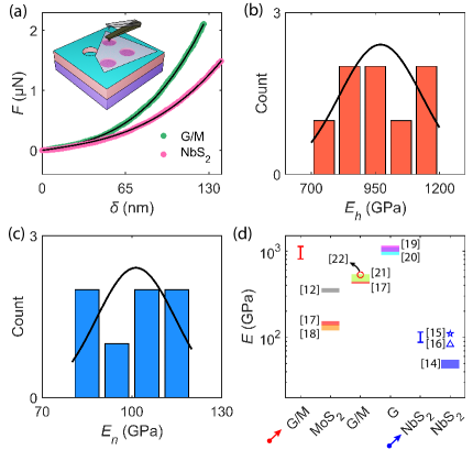
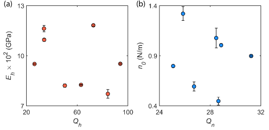
We extract and by the fitting the measured versus with Eq. S2 and Eq. 1, respectively, which nicely describe the experimental data for the NbS2 device D1 (pink points) and the heterostructure device D2 (green points) as shown in Fig. 2a. Figs. 2b and 2c show the extracted statistics of effective Young’s moduli for heterostructure devices () and Young’s moduli () for NbS2 devices, giving the mean values of and , respectively. In Fig. 2d, we compare and with values reported in the literature: shows a good agreement with the reported values of Sheraz et al. (2021); Sun, Agrawal, and Singh (2021); Sun, Zhuo, and Wu (2018); is between the reported values for MoS2 250 and graphene membranes 1025 Elder, Neupane, and Chantawansri (2015); Castellanos-Gomez et al. (2012); Bertolazzi, Brivio, and Kis (2011); López-Polín et al. (2015); Lee et al. (2008), but higher than the reported values for similar fully exfoliated heterostructures 461 Elder, Neupane, and Chantawansri (2015); Ye, Lee, and Feng (2017); Liu et al. (2014). The larger might be caused by the stronger interlayer adhesion or the larger intrinsic Young’s modulus of ALD MoS2. The standard deviations in extracted Young’s moduli, and for NbS2 and heterostructure resonators, respectively, are comparable to the ones reported in literature for exfoliated materials. This illustrates the high homogeneity of ALD materials.
In addition to the Young’s modulus, we also extract the pretension for each device. Supplementary tables 1 and 2 show a complete overview of the obtained parameters from the fitting to Eq. 1. The extracted ranges from 0.45 to for all heterostructure and NbS2 resonators, which are similar to values reported in the literature for resonators made by exfoliation and CVD Ye, Lee, and Feng (2017); Steeneken et al. (2021); Šiškins et al. (2022).
Let us now focus on the dynamics of the ALD resonators. We measured the dynamic response of the membranes with a laser interferometer Šiškins et al. (2022) (see Fig. 3a, bottom). A power modulated blue diode laser ( ) photothermally actuates the resonator, while the refection of a continuous-wave red He-Ne laser ( ) is sensitive to the time-dependent position of membrane. A vector network analyzer (VNA) provides a signal at drive frequency (OUT port) that modulates the blue laser intensity while the intensity of the red laser recorded by a fast photodiode is connected to the IN port. The VNA thus measures a signal that is proportional to the ratio of the membrane amplitude and actuation force. By sweeping the drive frequency , we locate the resonance peak in the range from to . Laser intensities are set to (blue) and (red), respectively. These intensities are low enough for the resonator to vibrate in the linear regime. All measurements were performed at room temperature in vacuum at a pressure of mbar.

Figure 3a (top inserts) shows the measured signal of NbS2 device D6, at around the fundamental and second resonance frequency, respectively. By fitting to the response function of a harmonic oscillator, we extract with and with . For vibrations of clamped drums, we can compute the resonance frequencies using Lee et al. (2013)
| (2) |
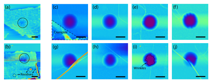
where is the areal mass density, is a correction factor of mass considering the contaminations on resonators, and is a mode-specific factor. We have for the fundamental mode and for the second mode. For an ideal membrane, in which is much larger than the flexural rigidity and thus , we have ; while for an ideal plate where is much larger than , we have and thus . The measured are and for heterostructure and NbS2 devices, respectively (see supplementary tables 1 and 2), suggesting that the modes of heterostructure resonators are near the membrane limit, while the modes of NbS2 resonators are in between the membrane and plate limit. We plot the extracted versus for all heterostructure resonators () and NbS2 resonators () in Figs. 3b and 3c, respectively, including the quality factor of the exfoliated graphene membranes before ALD. As expected from Eq. 2, decreases with increasing for the NbS2 resonators, while for heterostructure resonators varies widely from 14.6 to . This is attributed to the inhomogenieties like wrinkles and crumples in the heterostructures (see images in Fig. S1) and large differences in pretension. All measured resonance frequencies are comparable to those in literature reported for similar devices Lee et al. (2013); Castellanos-Gomez et al. (2012).
The extracted values of and are also comparable to values of previously studied resonators made by exfoliation and CVD Aguila et al. (2022); Zhu et al. (2022); Ye, Lee, and Feng (2017); Ye et al. (2021), as illustrated in Fig. 3f. To gain insight into the damping, we plot versus for heterostructure resonators and versus for NbS2 resonators, respectively, as plotted in Figs. 3d and 3e. For both cases, we observe a linear relation, indicating that pretension plays a more important role on damping than bending rigidity for heterostructure resonators, while it is on the other way around for NbS2 resonators. This is exactly as expected based on the ratio . On the other hand, we do not see clear relations of versus and versus as plotted in Fig. S2a and S2b, respectively.
Concerning the effective masses, we determine the correction factors and by substituting the measured , and the extracted and into Eq. 2 (see values in supplementary tables 1 and 2). We obtain and , respectively. The high of NbS2 devices is attributed to the contaminations from the PDMS stamping. The values for the heterostructure are surprisingly close or even below 1. This suggests the absence of any residues and possibly even the thinning of the graphene membrane during the ALD process, while the ALD MoS2 layer is mainly deposited on top of the suspended graphene membrane instead of bottom (see supplementary S2).
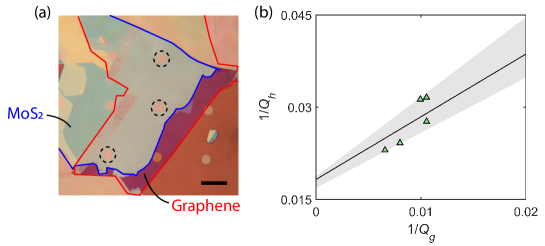
We also observe a general decrease of quality factor in heterostructure resonators after ALD (), as shown in Fig. 3b. Considering the dissipation mechanism for two parallel membranes, the overall can be modeled as
| (3) |
where can be different than 1 on account of structural changes in the graphene because of the ALD process, and is a fit parameter that represents the damping in the heterostructure originating from the ALD MoS2. We fit the measured versus with Eq. 3 (see Fig. 3g) and extract and . The fact that the obtained (within errors) is close to 1, provides evidence that there little to none increase of the dissipation in the graphene during the ALD process. A control experiment has been done with purely exfoliated graphene/MoS2 heterostructures (see Fig. S3), giving us and . The lower of ALD heterostructure compared to exfoliated layers can be attributed to a better conformality of the ALD layer and the absence of contamination by transfer polymers.
Although ALD is known to be capable of wafer-scale synthesis, the dimensions of our fabricated devices are still quite small due to the use of exfoliation in the fabricating process. A strategy could be to grow transferless suspended CVD 2D material membranes like graphene Pezone et al. (2022), and subsequently grow ALD material heterostructures from them. In addition, ALD could benefit from a method to precisely control the flatness, so as to avoid the cragged surfaces of nanoscale devices as illustrated in Figs. S1a and S1b.
In conclusion, we presented the fabrication and mechanical characterization of nanomechancial resonators consisting of ALD 2D materials. We developed two PEALD based approaches to suspend ALD flakes on a patterned Si/SiO2 substrate: one is dry transfer using PDMS (exfoliate ALD Nb2 flakes from glassy carbon); the other is ALD deposition of MoS2 on mechanically exfoliated suspended graphene drums. AFM indentation allows us to determine their Young’s moduli as and . Using an optomechanical method, we extracted their resonance frequencies and the corresponding quality factors. All of the above parameters are well comparable to the reported values of exfoliated and CVD resonators. We found experimental indications that the dissipation of ALD MoS2 membranes in heterostructures is roughly 3.7 times lower than that of purely exfoliated MoS2 membranes, which is promising for high-performance 2D heterostructure resonators. Our results show possibilities toward exploiting ALD technique for nanomechancial resonators in future explorations on atomically thin tunable resonators and 2D sensors. Meanwhile, the thickness-controllable ALD heterostructures could provide valuable insight in interactions at 2D interfaces, which can bring significant improvements in device performance and lead to new functionalities.
Conflict interest The authors declare that they have no competing financial interests.
Data Availability The data that support the findings of this study are available from the corresponding authors upon reasonable request.
References
- Barton et al. (2011) R. A. Barton, B. Ilic, A. M. Van Der Zande, W. S. Whitney, P. L. McEuen, J. M. Parpia, and H. G. Craighead, “High, size-dependent quality factor in an array of graphene mechanical resonators,” Nano letters 11, 1232–1236 (2011).
- Zhu et al. (2022) J. Zhu, B. Xu, F. Xiao, Y. Liang, C. Jiao, J. Li, Q. Deng, S. Wu, T. Wen, S. Pei, et al., “Frequency Scaling, Elastic Transition, and Broad-Range Frequency Tuning in WSe2 Nanomechanical Resonators,” Nano Letters (2022).
- Lee et al. (2013) J. Lee, Z. Wang, K. He, J. Shan, and P. X.-L. Feng, “High frequency MoS2 nanomechanical resonators,” ACS nano 7, 6086–6091 (2013).
- Steeneken et al. (2021) P. G. Steeneken, R. J. Dolleman, D. Davidovikj, F. Alijani, and H. S. Van Der Zant, “Dynamics of 2D material membranes,” 2D Materials 8, 042001 (2021).
- Lemme et al. (2020) M. C. Lemme, S. Wagner, K. Lee, X. Fan, G. J. Verbiest, S. Wittmann, S. Lukas, R. J. Dolleman, F. Niklaus, H. S. van der Zant, et al., “Nanoelectromechanical sensors based on suspended 2D materials,” Research 2020 (2020).
- Ye et al. (2021) F. Ye, A. Islam, T. Zhang, and P. X.-L. Feng, “Ultrawide frequency tuning of atomic layer van der Waals heterostructure electromechanical resonators,” Nano Letters 21, 5508–5515 (2021).
- Mackus, Bol, and Kessels (2014) A. Mackus, A. Bol, and W. Kessels, “The use of atomic layer deposition in advanced nanopatterning,” Nanoscale 6, 10941–10960 (2014).
- Sharma et al. (2018) A. Sharma, M. A. Verheijen, L. Wu, S. Karwal, V. Vandalon, H. C. Knoops, R. S. Sundaram, J. P. Hofmann, W. E. Kessels, and A. A. Bol, “Low-temperature plasma-enhanced atomic layer deposition of 2-D MoS2: Large area, thickness control and tuneable morphology,” Nanoscale 10, 8615–8627 (2018).
- Vos et al. (2016) M. F. Vos, B. Macco, N. F. Thissen, A. A. Bol, and W. Kessels, “Atomic layer deposition of molybdenum oxide from (NtBu)2(NMe2)2Mo and O2 plasma,” Journal of Vacuum Science & Technology A: Vacuum, Surfaces, and Films 34, 01A103 (2016).
- Hao, Marichy, and Journet (2018) W. Hao, C. Marichy, and C. Journet, “Atomic layer deposition of stable 2D materials,” 2D Materials 6, 012001 (2018).
- Basuvalingam et al. (2018) S. B. Basuvalingam, B. Macco, H. C. Knoops, J. Melskens, W. M. Kessels, and A. A. Bol, “Comparison of thermal and plasma-enhanced atomic layer deposition of niobium oxide thin films,” Journal of Vacuum Science & Technology A: Vacuum, Surfaces, and Films 36, 041503 (2018).
- Castellanos-Gomez et al. (2012) A. Castellanos-Gomez, M. Poot, G. A. Steele, H. S. Van Der Zant, N. Agraït, and G. Rubio-Bollinger, “Elastic properties of freely suspended MoS2 nanosheets,” Advanced materials 24, 772–775 (2012).
- Wang et al. (2019) G. Wang, Z. Dai, J. Xiao, S. Feng, C. Weng, L. Liu, Z. Xu, R. Huang, and Z. Zhang, “Bending of multilayer van der Waals materials,” Physical Review Letters 123, 116101 (2019).
- Sheraz et al. (2021) A. Sheraz, N. Mehmood, M. M. Çiçek, İ. Ergün, H. R. Rasouli, E. Durgun, and T. S. Kasırga, “High elasticity and strength of ultra-thin metallic transition metal dichalcogenides,” Nanoscale Advances 3, 3894–3899 (2021).
- Sun, Agrawal, and Singh (2021) H. Sun, P. Agrawal, and C. V. Singh, “A first-principles study of the relationship between modulus and ideal strength of single-layer, transition metal dichalcogenides,” Materials Advances 2, 6631–6640 (2021).
- Sun, Zhuo, and Wu (2018) Y. Sun, Z. Zhuo, and X. Wu, “Bipolar magnetism in a two-dimensional NbS2 semiconductor with high Curie temperature,” Journal of Materials Chemistry C 6, 11401–11406 (2018).
- Elder, Neupane, and Chantawansri (2015) R. M. Elder, M. R. Neupane, and T. L. Chantawansri, “Stacking order dependent mechanical properties of graphene/MoS2 bilayer and trilayer heterostructures,” Applied Physics Letters 107, 073101 (2015).
- Bertolazzi, Brivio, and Kis (2011) S. Bertolazzi, J. Brivio, and A. Kis, “Stretching and breaking of ultrathin MoS2,” ACS nano 5, 9703–9709 (2011).
- López-Polín et al. (2015) G. López-Polín, C. Gómez-Navarro, V. Parente, F. Guinea, M. I. Katsnelson, F. Perez-Murano, and J. Gómez-Herrero, “Increasing the elastic modulus of graphene by controlled defect creation,” Nature Physics 11, 26–31 (2015).
- Lee et al. (2008) C. Lee, X. Wei, J. W. Kysar, and J. Hone, “Measurement of the elastic properties and intrinsic strength of monolayer graphene,” science 321, 385–388 (2008).
- Ye, Lee, and Feng (2017) F. Ye, J. Lee, and P. X.-L. Feng, “Atomic layer MoS2-graphene van der Waals heterostructure nanomechanical resonators,” Nanoscale 9, 18208–18215 (2017).
- Liu et al. (2014) K. Liu, Q. Yan, M. Chen, W. Fan, Y. Sun, J. Suh, D. Fu, S. Lee, J. Zhou, S. Tongay, et al., “Elastic properties of chemical-vapor-deposited monolayer MoS2, WS2, and their bilayer heterostructures,” Nano letters 14, 5097–5103 (2014).
- Šiškins et al. (2022) M. Šiškins, S. Kurdi, M. Lee, B. J. Slotboom, W. Xing, S. Mañas-Valero, E. Coronado, S. Jia, W. Han, T. van der Sar, et al., “Nanomechanical probing and strain tuning of the Curie temperature in suspended Cr2Ge2Te6-based heterostructures,” npj 2D Materials and Applications 6, 1–8 (2022).
- Aguila et al. (2022) M. A. C. Aguila, J. C. Esmenda, J.-Y. Wang, T.-H. Lee, C.-Y. Yang, K.-H. Lin, K.-S. Chang-Liao, S. Kafanov, Y. A. Pashkin, and C.-D. Chen, “Fabry–Perot interferometric calibration of van der Waals material-based nanomechanical resonators,” Nanoscale Advances 4, 502–509 (2022).
- Pezone et al. (2022) R. Pezone, G. Baglioni, P. M. Sarro, P. G. Steeneken, and S. Vollebregt, “Sensitive Transfer-Free Wafer-Scale Graphene Microphones,” ACS Applied Materials & Interfaces (2022).
- Sharma et al. (2020) A. Sharma, R. Mahlouji, L. Wu, M. A. Verheijen, V. Vandalon, S. Balasubramanyam, J. P. Hofmann, W. E. Kessels, and A. A. Bol, “Large area, patterned growth of 2D MoS2 and lateral MoS2–WS2 heterostructures for nano-and opto-electronic applications,” Nanotechnology 31, 255603 (2020).
Supplementary Materials
S1: AFM indentation measurements on fabricated ALD resonators
We fit the measured curves of versus to extract the pretension and Young’s modulus of the fabricated resonators. The applied force equals the product of the cantilever stiffness and its deflection . We use a cantilever with 53.7 , and repeat the indentation measurement three times for each device.
The classical relation for the bending rigidity, , in general, is not valid for multilayer 2D materials, where the interlayer shear interactions are weak and slippage is inevitable. As a result, a calibration factor is induced to describe this interaction, giving the formula as . Since the layers number of graphene and MoS2 in the fabricated heterostructures are 40 and 13 roughly, we adopt and from literature Wang et al. (2019), respectively. We also assume due to their similar lattice structures. For NbS2 resonators, we can directly fit the measured versus to Eq. 1 to obtain and . However, for heterostructure resonators, considering the different mechanical properties of graphene and MoS2 layers, their effective Young’s modulus and effective bending rigidity are given by Ye, Lee, and Feng (2017); Šiškins et al. (2022)
| (S1) |
respectively, where . As a result, the relation of versus for heterostructure resonators is expressed as
| (S2) |
Using the values of , , , , and , the part inside parenthesis of the first term in Eq. S2 can be rewritten as . This part is then replaced by and separately in the fit, causing only a deviation to the extracted .
S2: Experimental results of nanomechanical characteristics for all fabricated ALD resonators in this work
TABLE 1 gives the measured parameters of all ALD heterostructure devices, including radius of drums, Young’s modulus , pretension , fundamental resonance frequency and (corresponding to the graphene membrane before ALD), quality factor and , modes ratio , and the calibration factor with respect to the mass of membrane. TABLE 2 gives the measured parameters of all ALD NbS2 devices. We cannot extract a precise value of for device D8 due to its small size, which needs a quite large loading to achieve the effective indentation with cubic regime. The second resonance frequency of device D8 is missed as well, since we use a low pass filter (up to ) on VNA during the dynamic measurements.
Note that in the calculation of for heterostructure resonators, we have already used the relation , where the thickness of ALD MoS2 is determined by scanning the scratch of MoS2 layer on Si/Si2 substrate. We assume that ALD MoS2 mainly grows on top of the graphene membrane, since the average value of in TABLE 1 is close to 1, indicating that the thickness of ALD MoS2 layer in heterostructure is roughly equal to that on substrate. For heterostructure devices D4 and D5, is larger than 1, which might result from a small quantity of ALD MoS2 deposited on the bottom of graphene.
Figure S1 shows the AFM scanning images of ALD NbS2 device D1 and D2, as well as all ALD heterostructure devices. We can observe the visible polymer residues, crumples and wrinkles on these devices, which significantly affect their static and dynamic properties. More details about the TEM images of ALD MoS2 can be found in our previous work Sharma et al. (2020).
| Device | () | () | () | () | ||||
|---|---|---|---|---|---|---|---|---|
| D1 | 951.7 | 1.418 | 8.3 | 100.6 | 23.5 | 84.2 | 1.41 | 1.16 |
| D2 | 771.4 | 1.547 | 13.6 | 99.1 | 30.7 | 94.0 | 1.49 | 0.61 |
| D4 | 825.5 | 1.074 | 8.5 | 63.2 | 16.2 | 33.9 | 1.58 | 2.03 |
| D5 | 1095.7 | 1.293 | 9.0 | 57.5 | 14.6 | 34.0 | 1.71 | 3.23 |
| D6 | 1182.6 | 1.462 | 7.6 | 125.9 | 22.9 | 72.8 | 1.53 | 1.44 |
| D7 | 950.7 | 1.318 | 8.4 | 99.4 | 28.3 | 63.0 | 1.67 | 0.78 |
| D8 | 1162.9 | 0.892 | 10.2 | 33.6 | 25.8 | 26.4 | 1.92 | 1.01 |
| D10 | 820.9 | 1.010 | 12.4 | 43.0 | 35.0 | 50.3 | 1.45 | 0.43 |
| Device | () | () | () | () | |||
|---|---|---|---|---|---|---|---|
| D1 | 4 | 116.3 | 0.899 | 12.4 | 31.2 | 1.81 | 2.05 |
| D2 | 4 | 101.8 | 0.447 | 11.2 | 28.6 | 2.26 | 2.12 |
| D3 | 4 | 96.5 | 0.593 | 10.8 | 26.7 | 1.58 | 2.20 |
| D4 | 3 | 87.5 | 1.320 | 15.2 | 25.9 | 1.67 | 3.30 |
| D5 | 3 | 106.7 | 1.077 | 15.8 | 28.5 | 1.72 | 3.60 |
| D6 | 3 | 117.5 | 1.005 | 16.0 | 28.9 | 1.57 | 3.79 |
| D7 | 3 | 83.2 | 0.797 | 15.1 | 25.1 | 3.10 | 3.05 |
| D8 | 2 | 21.0 | 32.7 |
Figures S2a and S2b give the obtained versus for heterostructure resonators and versus for NbS2 resonators, respectively. Unlike the proportional relations shown in Figs. 3b and 3c in the main text, we see versus and versus are irregular here.
S3: Experimental results of quality factors for purely exfoliated graphene/MoS2 heterostructure resonators
To shed light on the energy dissipation of MoS2 layer in the heterostructure, purely exfoliated graphene/MoS2 heterostructure devices are fabricated (Fig. S3a) and measured in interferometry setup. As plotted in Fig. S3b, the measured versus is fitted with Eq. 3 and thus extract and .