Transverse currents in spin transistors
Abstract
In many systems, planar Hall effect wherein transverse signal appears in response to longitudinal stimulus is rooted in spin-orbit coupling. A spin transistor put forward by Datta and Das on the other hand consists of ferromagnetic leads connected to spin-orbit coupled central region and its conductance can be controlled by tuning the strength of spin-orbit coupling. We find that transverse currents also appear in Datta-Das transistors made by connecting two two-dimensional ferromagnetic reservoirs to a central spin-orbit coupled two-dimensional electron gas. We find that the spin transistor exhibits a nonzero transverse conductivity which depends on the direction of polarization in ferromagnets and the location where it is measured. We study the conductivities for the system with finite and infinite widths. The conductivities exhibit Fabry-Pérot type oscillations as the length of the spin-orbit coupled regions is varied. Interestingly, even in the limit when longitudinal conductivity is made zero by cutting off the junction between the central spin-orbit coupled region and the ferromagnetic lead on one side (right), the transverse conductivities remain nonzero in the regions that are on the left side of the cut-off junction.
I Introduction
In a two-dimensional metal, a transverse voltage results in response to a current in presence of a magnetic field normal to the plane of the metal, an effect known as Hall effect Kittel (2005). This is due to Lorentz force on electrons in the metal. It was found that in certain systems, the voltage developed perpendicular to the current, magnetic field and the current - all three can lie in the same plane, an effect known as planar Hall effect Goldberg and Davis (1954); Tang et al. (2003); Roy and Kumar (2010); Annadi et al. (2013); Taskin et al. (2017); He et al. (2019); Bhardwaj et al. (2021); Burkov (2017); Kumar et al. (2018); Sonika et al. (2021). While in many of these systems Goldberg and Davis (1954); Tang et al. (2003); Annadi et al. (2013), the planar Hall effect is due to spin-orbit coupling (SOC), the origin is rooted in chiral anomaly in some other systems Burkov (2017); Kumar et al. (2018). In topological insulators, spin momentum locking - which is qualitatively same as SOC, causes this effect Suri and Soori (2021). In spin-orbit coupled metals, the transverse deflection of the longitudinal current under the influence of Zeeman field explains planar Hall effect Soori (2021). A closely related phenomenon - “in-plane Hall effect” rooted in Berry curvature and band geometric effects has also been reported recently Liang et al. (2018); Zhou et al. (2022); Wang et al. (2022).
Datta-Das transistor proposed in 1990 makes use of the fact that the electron spin precesses in spin-orbit coupled region Datta and Das (1990). Experimentally, it was challenging to realize such a transistor, since good quality systems with Rashba spin split bands and spin polarized electrons in semiconductors were difficult to achieve. It was demonstrated in 1997 that the strength of SOC in a semiconductor can be tuned by an applied gate voltage Nitta et al. (1997). The first version of spin transistor proposed by Datta and Das was realized in 2009 Koo et al. (2009). Around the same time, transverse signal was detected in spin-orbit coupled systems by injecting spin polarized electrons Wunderlich et al. (2009). Later, improved versions of Datta-Das transistor were developed Chuang et al. (2015); Choi et al. (2015). In the improved versions Chuang et al. (2015); Choi et al. (2015), the transport was ballistic, in contrast to the diffusive transport in the earlier versions Koo et al. (2009); Wunderlich et al. (2009). Transport in Datta-Das transistor has also been investigated theoretically Aharony et al. (2019); Sarkar et al. (2020).
In ‘planar Hall effect’, the transverse voltage is due to deflection of longitudinal current in the spin-orbit coupled region by the application of in-plane Zeeman field. It would be interesting to investigate whether there is a transverse deflection in the spin-orbit coupled region when the injected electrons are spin-polarized, instead of using a Zeeman field. In this work, we explore the possibility of a transverse current in response to a bias in a ferromagnet-spin-orbit coupled region-ferromagnet junction, where the two ferromagnets are parallel. We follow Landauer-Büttiker scattering approach generalized to two-dimensional systems to address this problem Landauer (1957); Büttiker et al. (1985); Datta (1995). We find that the value of transverse conductivity depends on the location and the spin polarization of the ferromagnets. We study infinitely wide systems as well as the ones having finite width. Further, we find that the transverse conductivity is nonzero even in the case when the one of the junctions between the spin-orbit coupled region and the ferromagnet is cut-off and the longitudinal conductivity is zero.
II Details of calculation
The Hamiltonian describing the setup depicted in Fig. 1 is
| (1) | |||||
where . Here, is the effective mass of electrons in the system, -the chemical potential, -the strength of SOC, -the magnitude of the Zeeman energy that characterizes the ferromagnet, -the direction of spin polarization of the ferromagnets and are Pauli spin matrices. The region is spin-orbit coupled region. The regions and are ferromagnetic wherein the electrons are spin polarized. Along -direction the system is assumed to be translationally invariant. Current is conserved at the junctions for very general boundary conditions other than continuity of wavefunction and the derivatives, akin to the problem of point like scatterer in one dimension Soori (2023). Here we choose the wavefunction and the derivatives to satisfy
| (2) |
at where and . Here, is a real constant. The value implies that the junction is cut off at . In the ferromagnetic leads ( and ), the dispersion relations are , and if , near zero energy, only one band exists. We shall consider transport in the energy range where only one band actively participates in the transport. In this energy range, the spins of the plane wave modes in the ferromagnet are polarized in a direction . In the spin-orbit coupled region (), the dispersion is , where . The width in the -direction can be either finite or infinite. For a finite with periodic boundary conditions in -direction, the is quantized whereas in the limit of , takes continuous values and the electron can be incident at any angle .
II.1
The wavefunction of an electron that approaches from the left ferromagnet onto the SOC region at energy making an angle with -axis has the form (where and ) with
| (3) | |||||
where and are eigenspinors of with , , for are given by , , , and , with for , and , . The boundary conditions at , can be utilized to determine the scattering amplitudes- . The differential conductivity which is defined as where and are infinitesimal changes in current density along -direction and the bias respectively, is given by
| (4) |
Here, is evaluated at energy .
The net current in the -direction can also have a nonzero value. Transverse conductivity defined as where is the infinitesimal change in current density along -direction is given by
| (5) |
where is the current density along -direction for angle of incidence at location . The current density along -direction depends on - the location in the longitudinal direction and angle of incidence . It is given by
II.2 Finite
For finite width with periodic boundary conditions, takes values that are integer multiples of . At energy , the modes that contribute to transport are the ones with where takes integer values in the range , ( denotes the maximum integer less than or equal to ), . The wavefunction for an electron incident in a mode with a given takes the form with
| (7) | |||||
where . The notation is similar to the one followed next to eq. (3), except that the scattering coefficients depend on the index that dictates the value of . The differential conductivity is given by the expression
| (8) |
The transverse conductivity is given by the expression
| (9) |
where
| (10) | |||||
Note that here depend on .
III Results and Analysis
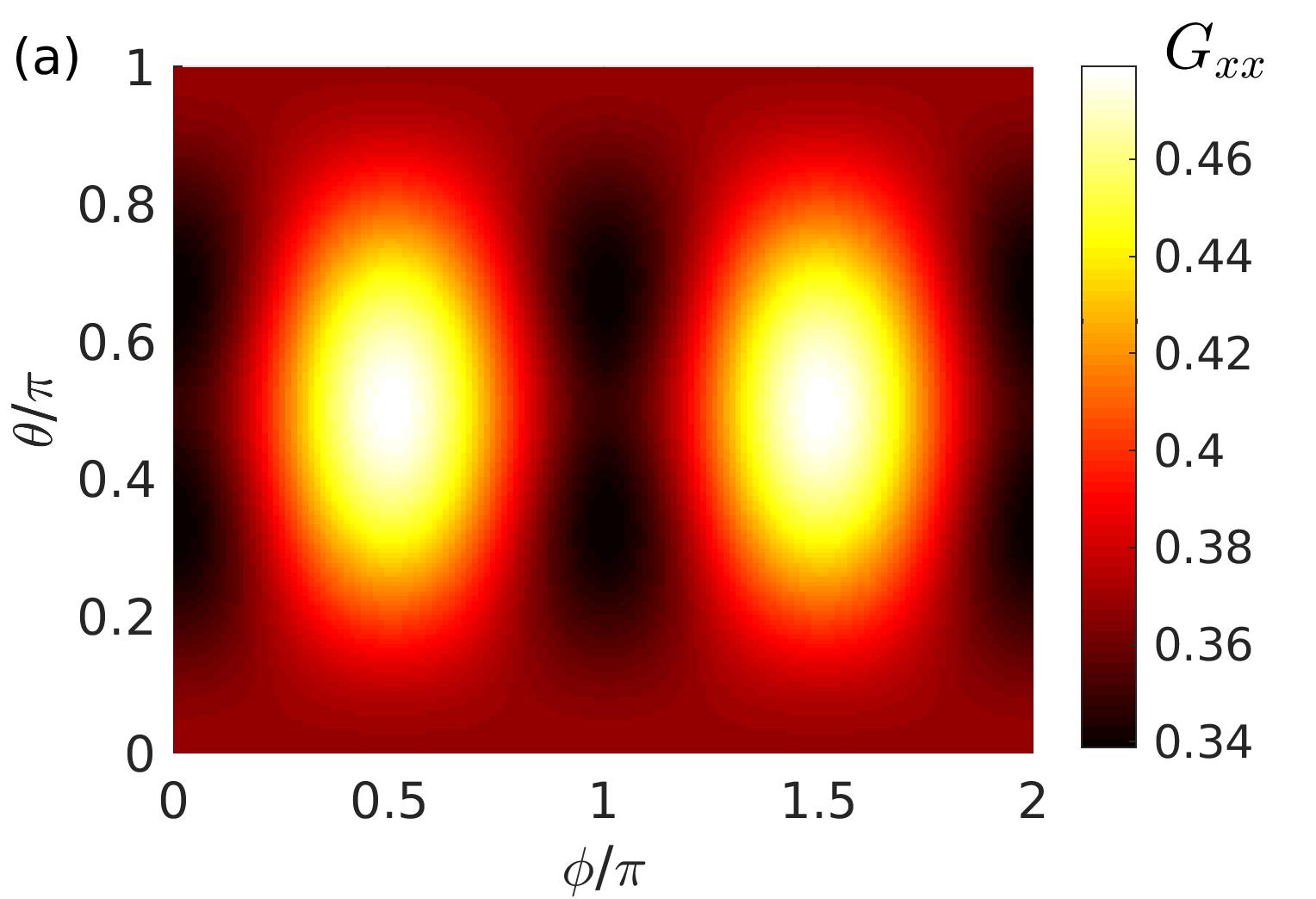
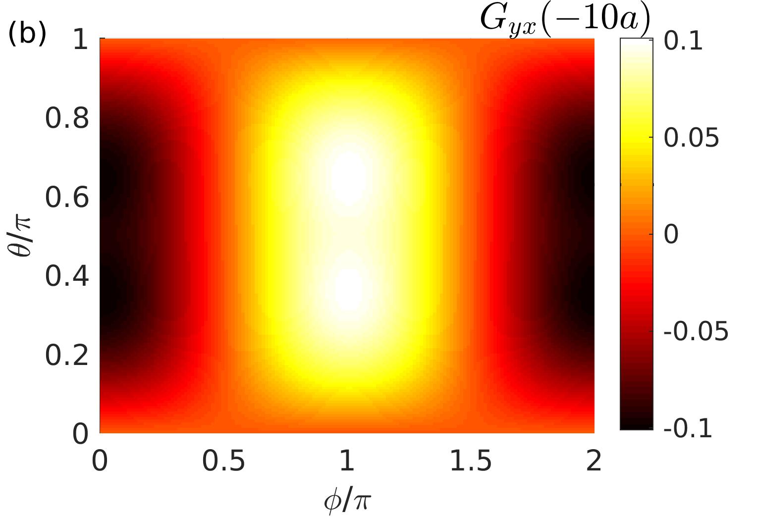
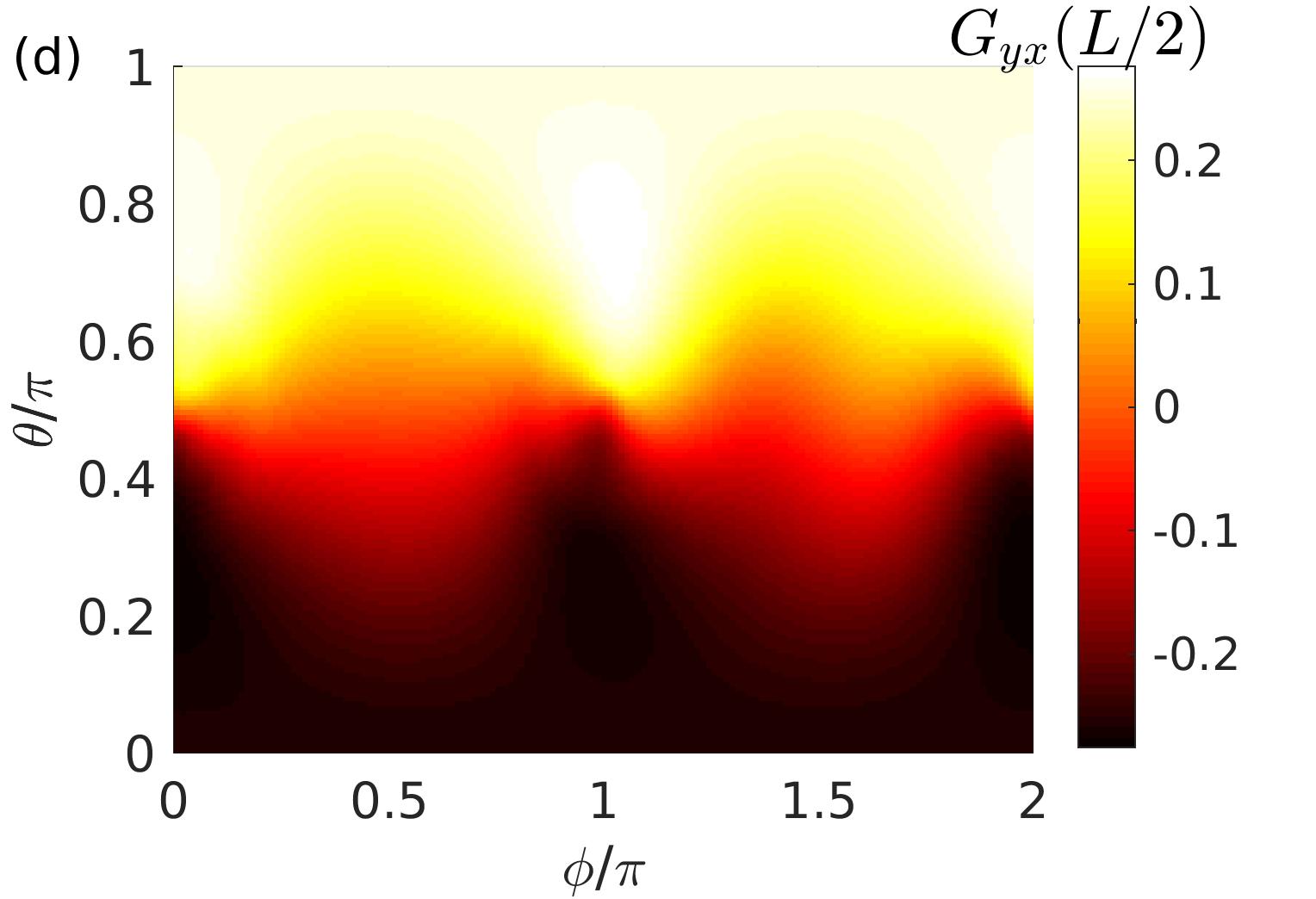
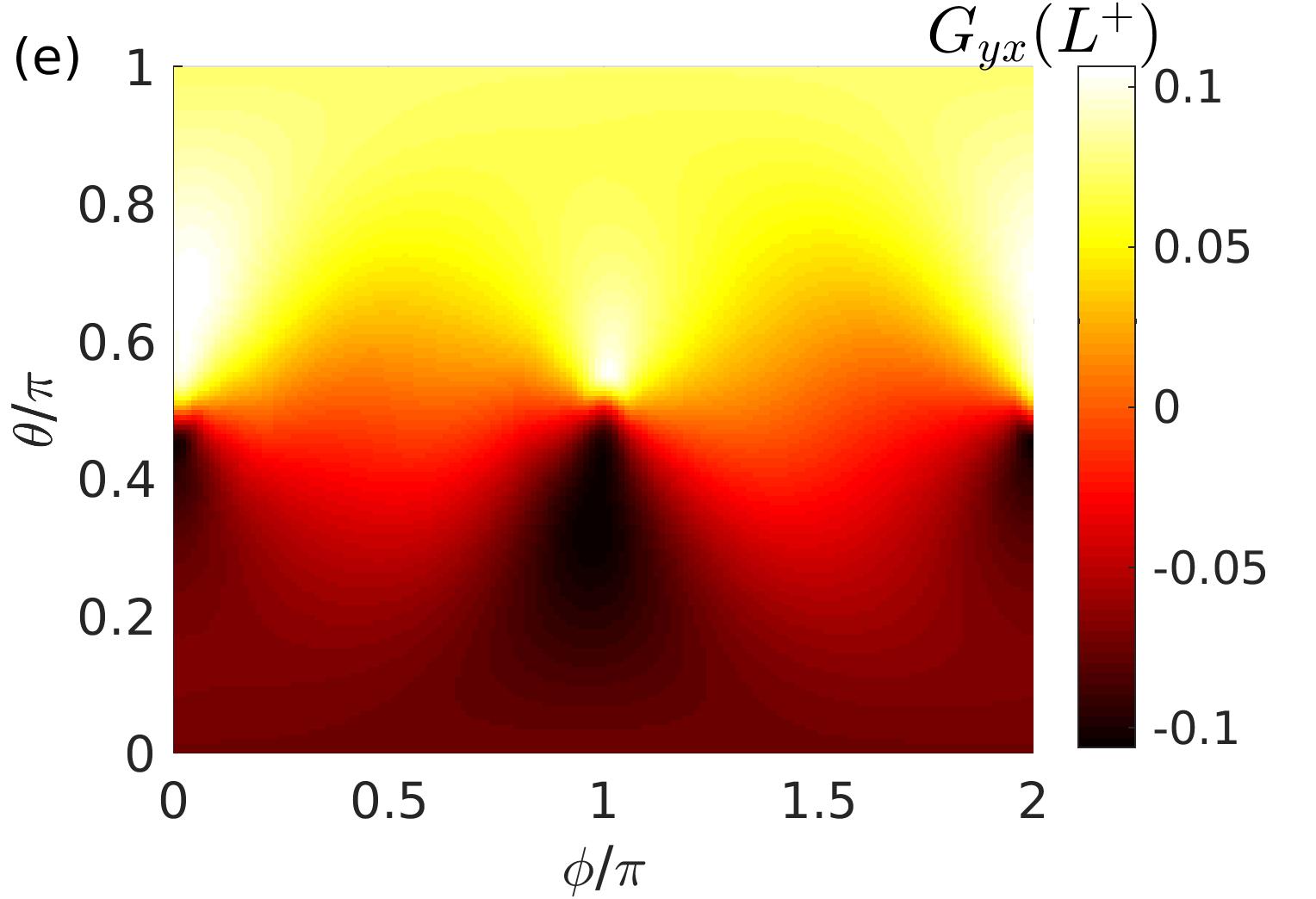
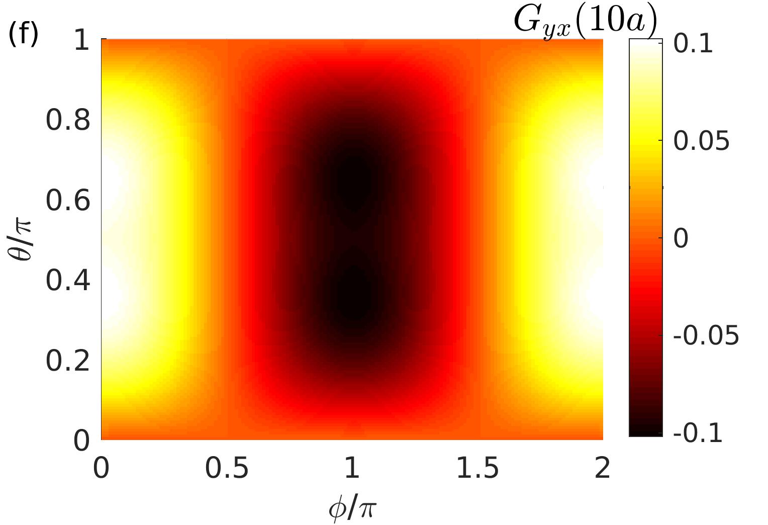
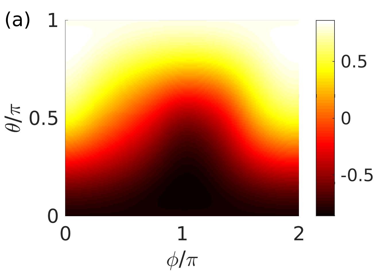
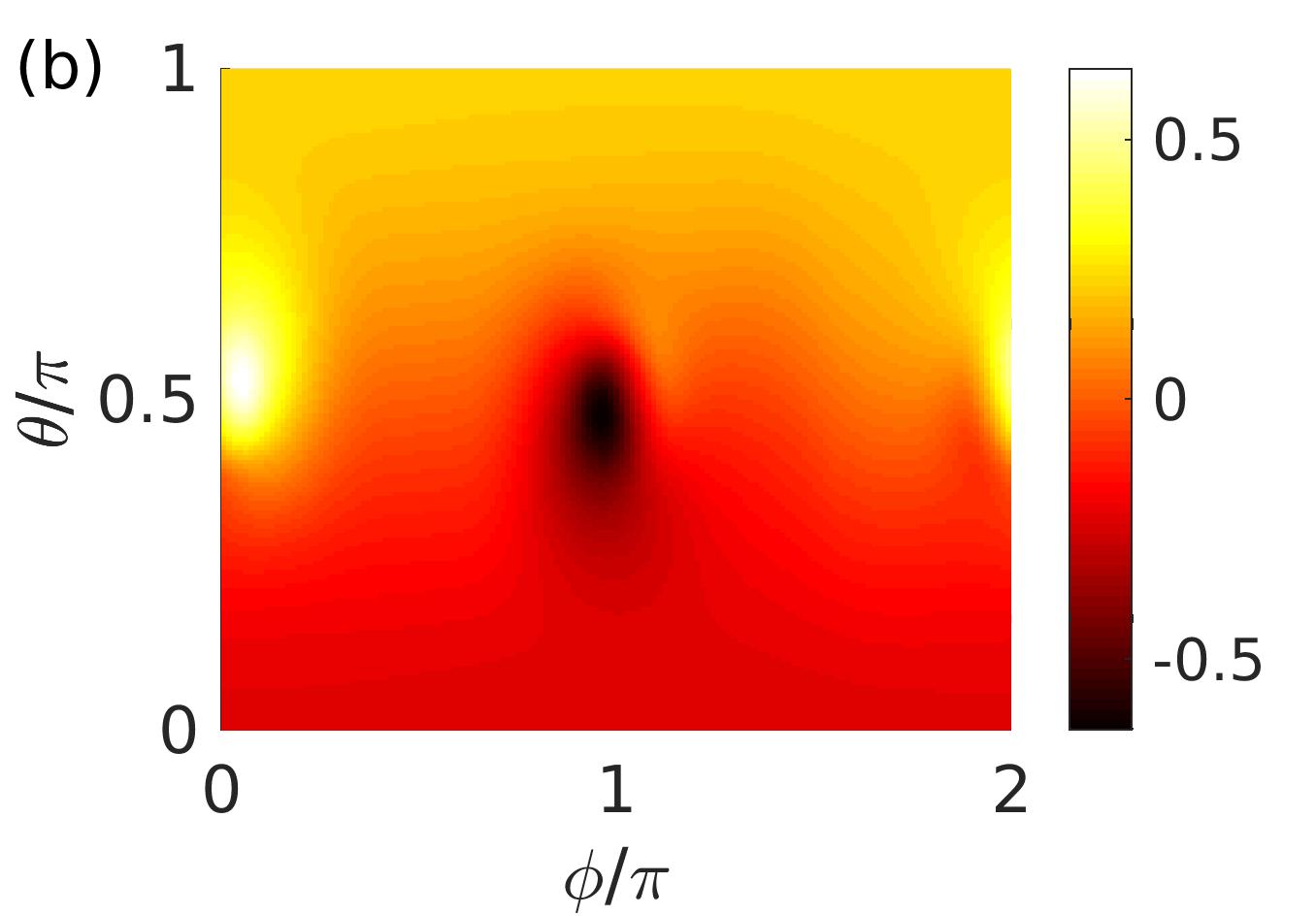
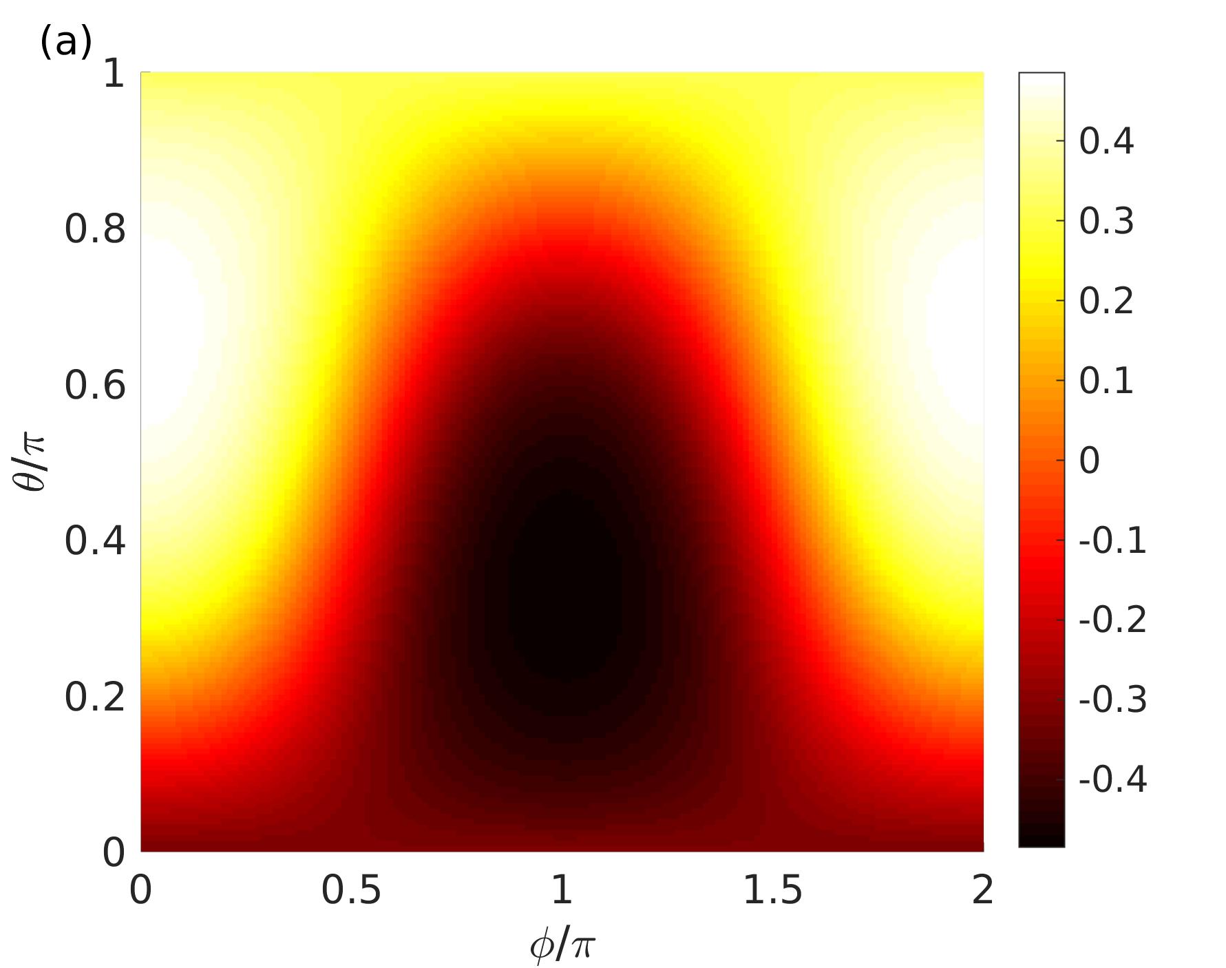
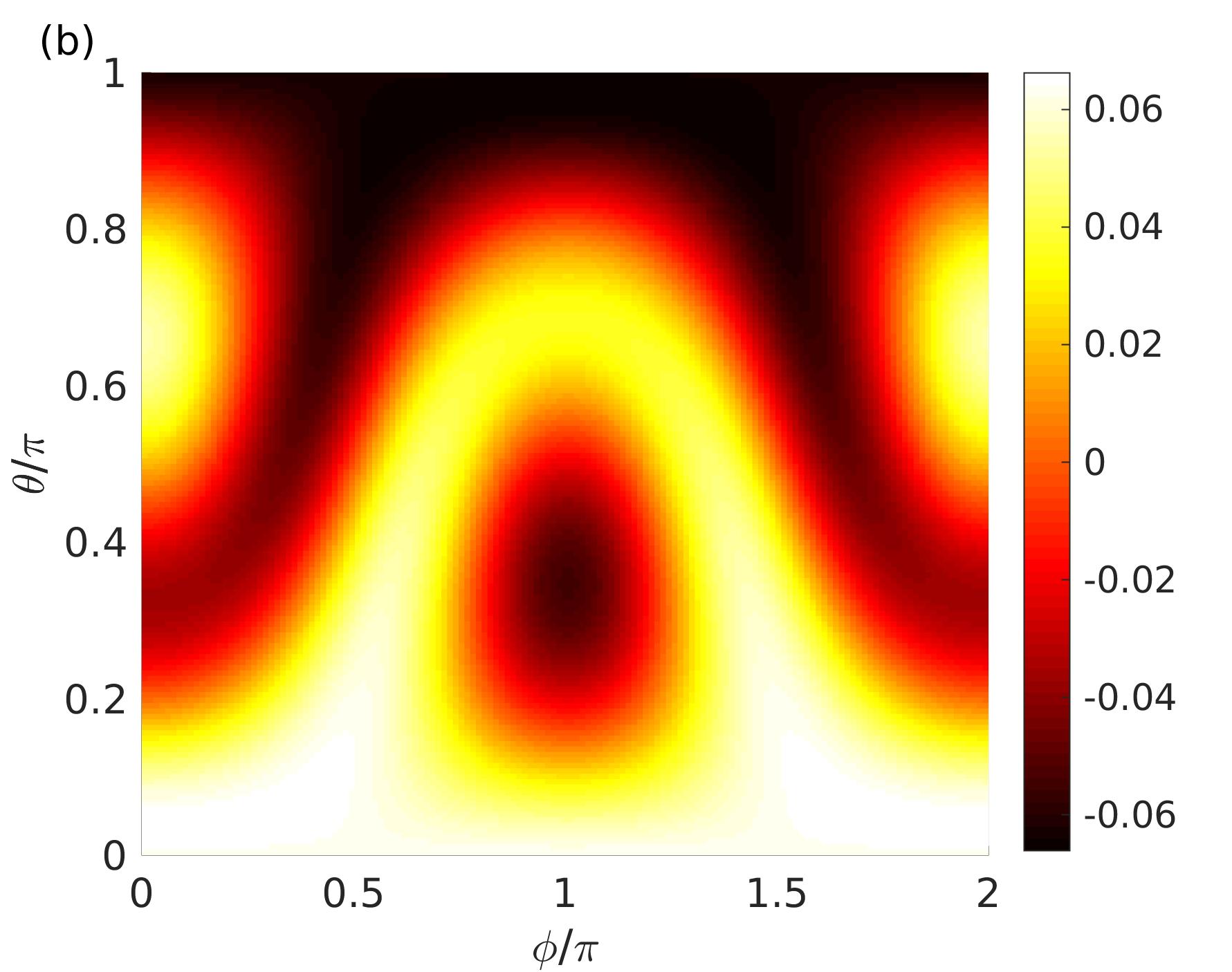
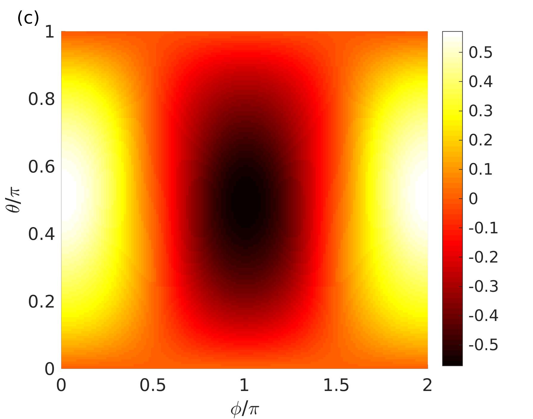
We choose , , (where ), , and calculate the conductivity and the transverse conductivity at numerically as functions of and and plot in Fig. 2. Here zero bias conductivity means the ratio of tiny current density as a response to a tiny bias in the limit . The conductivity depends on the spin polarization direction of the ferromagnet [see Fig. 2(a)] - a characteristic feature of Datta-Das spin transistor. When the spin polarization in the leads is along -direction, the incident electron spin is the same as the spin of the electrons moving along direction in the spin-orbit coupled region, which contributes the most to the longitudinal conductivity. Hence, is peaked around and in Fig. 2(a). In Fig. 2(b-f), the transverse conductivities at different locations are plotted as functions of . The value of transverse conductivity depends on the location and the polarization direction. The dependence on the polarization direction is because of the SOC in the central region. The SOC term in the Hamiltonian is . Any spin component will imply that the transverse wave numbers and are inequivalent and the scattering probabilities are different for these transverse wave numbers. The transverse conductivity is integral of over . depends on through the wavefunction as shown in eq. (LABEL:eq:Iy) and if the scattering amplitudes change when goes to , acquires a nonzero value.
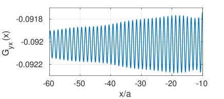
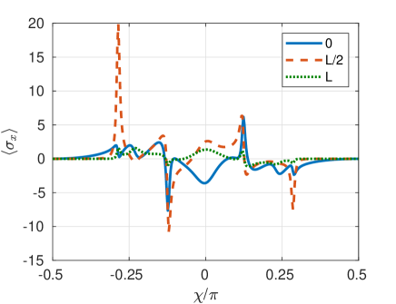
A particularly interesting case is for for which, the ferromagnets are polarized with a zero value for . This means that for , the transverse conductivity should be zero. While this holds true at , the transverse conductivities at locations are nonzero [see Fig.2(b-f)]. The reason for this feature is in the wavefunction which also has evanescent modes pointing along that decay away from the spin-orbit coupled region, but are present near the junctions at as can be seen from eq. (3). We plot using the wavefunction at locations as a function of angle of incidence for and in Fig. 3. We find that not only is nonzero at , it is not an odd function of and when is integrated over , the transverse conductivity obtained is not zero for . The transverse conductivity in the regions and is not affected by the interference of the evanescent modes with the plane waves and meets the expectation that when , .
Another feature of the transverse conductivity is that, while independent of for , oscillates with for . This is because, for , and for , . From eq. (LABEL:eq:Iy), it can be seen that the transverse conductivity depends on , which in turn depends on for . In Fig. 4, is plotted versus for and keeping other parameters the same. It can be seen that the transverse conductivity is not periodic in in the region even though it oscillates. These oscillations of transverse conductivity are rooted in density modulations that are akin to Friedel oscillations.
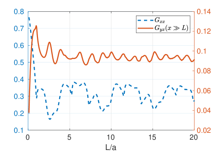
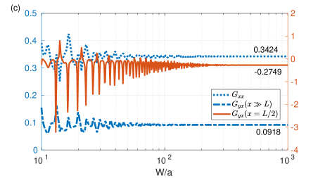
We now study the dependence of and on the length of the spin-orbit coupled region . In Fig. 5, we plot the two conductivities versus the length for and keeping other parameters same as before. We find that the both the conductivities oscillate with though not perfectly in a periodic fashion. Such an oscillation of conductivities is reminiscent of Fabry-Pérot type interference Liang et al. (2001); Ofek et al. (2010); Soori et al. (2012); Soori and Mukerjee (2017); Nehra et al. (2019); Soori (2019); Suri and Soori (2021); Soori (2021, 2022); Soori et al. (2023). In similar one dimensional systems, the peaks in conductance versus graph are uniformly spaced. Because, the Fabry-Pérot resonance condition is , where is the difference between two consecutive peak positions. However, the conductivities in Fig. 5 are calculated by taking integral of angles of incidence in the range [see eq. (4) and eq. (5)]. For different values of angle of incidence , is different. This is the reason why the peaks in Fig. 5 are not uniformly spaced. For the parameters chosen, the wavenumbers in the SOC region for normal incidence at are . This means, . On inspection, the average in Fig. 5 is for and for , which approximately agree with from Fabry-Pérot resonance condition for normal incidence.
Next, we focus our attention on the case of finite width. The formulae in eq. (8) and eq. (9) are used to calculate the conductivities numerically. In Fig. 6(a,b), the transverse conductivity at is plotted versus for keeping other parameters same as earlier. For , the plot of transverse conductivity versus (not shown) looks similar to Fig. 2 (d) which corresponds to the transverse conductivity in the limit of infinite width , whereas for , the transverse conductivity plots do not resemble the one for infinite width. In Fig. 6(c), the conductivities , and are plotted as functions of the width for the choice and . We find that the saturation values of the conductivities in the limit of large () agree with the respective conductivities calculated for the case of .
When the junction between spin-orbit coupled region and the ferromagnet at is cut-off by taking in the boundary condition given by eq. (2), the longitudinal conductivity is zero. In this limit, we calculate the transverse conductivities in the region . Zero bias transverse differential conductivities at are plotted as functions of in Fig. 7(a,b,c). It is interesting to see that the transverse conductivities can be nonzero even when the longitudinal conductivity is zero. This is due to a combination of spin-polarization of incident electrons and spin orbit coupling in the central region.
IV Discussion
Transverse currents are due to spin polarised electrons injected into the spin orbit coupled region. So, in the case when the region to the right of SOC region is a normal metal with no spin polarization instead of a ferromagnet, transverse currents are expected. In fact, even in the extreme case that there is nothing on the right side of SOC region (which is same as cutting of the right junction), transverse currents will appear.
The spin Hall effect involves the generation of a transverse spin current and spin accumulation at the edges in the transverse direction as a result of a charge current flowing in the longitudinal direction Murakami et al. (2003); Sinova et al. (2004, 2015). On contrary, in inverse spin Hall effect, a spin current will result in transverse charge current Sinova et al. (2015). The transverse current we found in this study is similar in spirit to inverse spin Hall effect. In such effects, spin Hall angle - the ratio of dimensionless charge current to dimensionless spin current determines the extent of spin to charge conversion. The longitudinal current is spin current, since the leads are fully spin polarized. So, the spin Hall angle is the ratio of transverse to the longitudinal conductivities. From Fig. 2, it can be seen that the spin Hall angle depends on the location at which the transverse conductivity is calculated. Spin Hall angle reaches a maximum value of around as can be seen from Fig. 2. For the case of the right junction being cut-off wherein the spin current is zero, the spin Hall angle shoots up to infinity.
An earlier work Sarkar et al. (2020) finds zero transverse currents. The main difference between their model and ours is that in their model, the spin-orbit coupled region is one-dimensional whereas in our work the spin-orbit coupled region is two-dimensional. Having two-dimensional spin-orbit coupled region is essential for getting nonzero transverse conductivity. In the limit of small for which there is only one transport channel (), we find that the transverse conductivity is zero in all regions.
Spin-orbit coupling can be induced in graphene by proximitizing it with transition metal dichalcogenides Belayadi and Vasilopoulos (2022, 2023). Inducing ferromagnetism in graphene has also been discussed in literature Haugen et al. (2008); Soori et al. (2018). While the strength of spin-orbit coupling in Datta-Das transistor is varied to control the conductance, gate voltage can be used to control the conductances in graphene heterostructures Belayadi and Vasilopoulos (2022). It will be an interesting future direction to explore transport in spin transistors designed on graphene due to its high electron mobility and the Dirac nature. Our calculations can be repeated using the Dirac Hamiltonian for graphene with terms added for spin-orbit coupling and ferromagnetism to model Datta-Das transistor on graphene.
V Summary and Conclusion
We have theoretically studied longitudinal and transverse conductivities in a spin transistor consisting of ferromagnets and a two-dimensional electron gas with Rashba SOC using Landauer-Büttiker approach. We have shown that the transverse conductivity can be non-zero and depends on the location where it is calculated, in addition to the direction of spin polarization of the ferromagnets. When the spin polarization component along in the ferromagnets is zero, the transverse conductivity is expected to be zero since the SOC is of Rashba type. However, we find that the transverse conductivity is nonzero in and around the spin-orbit coupled region. This is because of the presence of decaying modes in the ferromagnet pointing opposite to the spin polarization direction near the junctions. We explain this qualitatively by showing that near the junctions as a function of angle of incidence is not an odd function. The transverse conductivity oscillates with the location in the source electrode, since the probability density oscillates in the source region. The conductivities oscillate as a function of the length of the spin-orbit coupled region due to Fabry-Pérot interference. However, the oscillation is not perfectly periodic, since the conductivities have contributions from all possible angles of incidence. We also study the case of the system with a finite width. The conductivities oscillate as a function of the width for small and intermediate widths and for large width, saturate to the respective conductivities calculated for infinite width limit. Finally, we find that the transverse conductivity can be nonzero even in the limit when the longitudinal conductivity is zero.
Our findings can be tested in devices wherein the components that make the transistor are ballistic. In early experimental realizations of the spin transistors Koo et al. (2009); Wunderlich et al. (2009), the spin-orbit coupled regions were diffusive. The versions of spin transistors realized later Chuang et al. (2015); Choi et al. (2015) employed materials wherein the transport is ballistic. With the development of high quality ballistic devices in recent times, we envisage that our predictions can be put to test.
Acknowledgements.
We thank DST-INSPIRE Faculty Award (Faculty Reg. No. : IFA17-PH190) for financial support. We thank Dhavala Suri, Amnon Aharony and Kingshuk Sarkar for stimulating discussions.References
- Kittel (2005) C. Kittel, Introduction to Solid State Physics, 8th ed. (John Wiley & Sons Inc., 2005).
- Goldberg and Davis (1954) C. Goldberg and R. E. Davis, “New galvanomagnetic effect,” Phys. Rev. 94, 1121–1125 (1954).
- Tang et al. (2003) H. X. Tang, R. K. Kawakami, D. D. Awschalom, and M. L. Roukes, “Giant planar Hall effect in epitaxial (Ga,Mn)As devices,” Phys. Rev. Lett. 90, 107201 (2003).
- Roy and Kumar (2010) A. Roy and P. S. A. Kumar, “Giant planar Hall effect in pulsed laser deposited permalloy films,” J. Phys. D 43, 365001 (2010).
- Annadi et al. (2013) A. Annadi, Z. Huang, K. Gopinadhan, X. Renshaw Wang, A. Srivastava, Z. Q. Liu, H. Harsan Ma, T. P. Sarkar, T. Venkatesan, and Ariando, “Fourfold oscillation in anisotropic magnetoresistance and planar Hall effect at the heterointerfaces: Effect of carrier confinement and electric field on magnetic interactions,” Phys. Rev. B 87, 201102 (2013).
- Taskin et al. (2017) A. A. Taskin, H. F. Legg, F. Yang, S. Sasaki, Y. Kanai, K. Matsumoto, A. Rosch, and Y. Ando, “Planar Hall effect from the surface of topological insulators,” Nat. Commun. 8, 1340 (2017).
- He et al. (2019) P. He, S. S.-L. Zhang, D. Zhu, S. Shi, O. G. Heinonen, G. Vignale, and H. Yang, “Nonlinear planar Hall effect,” Phys. Rev. Lett. 123, 016801 (2019).
- Bhardwaj et al. (2021) A. Bhardwaj, P. S. Prasad, K. Raman, and D. Suri, “Observation of planar Hall effect in topological insulator – ,” Appl. Phys. Lett. 118, 241901 (2021).
- Burkov (2017) A. A. Burkov, “Giant planar Hall effect in topological metals,” Phys. Rev. B 96, 041110 (2017).
- Kumar et al. (2018) N. Kumar, S. N. Guin, C. Felser, and C. Shekhar, “Planar Hall effect in the Weyl semimetal ,” Phys. Rev. B 98, 041103 (2018).
- Sonika et al. (2021) Sonika, M. K. Hooda, S. Sharma, and C. S. Yadav, “Planar Hall effect in Cu intercalated PdTe2,” Appl. Phys. Lett. 119, 261904 (2021).
- Suri and Soori (2021) D. Suri and A. Soori, “Finite transverse conductance in topological insulators under an applied in-plane magnetic field,” J. Phys.: Condens. Matter 33, 335301 (2021).
- Soori (2021) A. Soori, “Finite transverse conductance and anisotropic magnetoconductance under an applied in-plane magnetic field in two-dimensional electron gases with strong spin–orbit coupling,” J. Phys.: Condens. Matter 33, 335303 (2021).
- Liang et al. (2018) T. Liang, J. Lin, Q. Gibson, S. Kushwaha, M. Liu, W. Wang, H. Xiong, J. A. Sobota, M. Hashimoto, P. S. Kirchmann, Z-X. Shen, R. J. Cava, and N. P. Ong, “Anomalous Hall effect in ZrTe5,” Nat. Phys. 14, 451–455 (2018).
- Zhou et al. (2022) J. Zhou, W. Zhang, Y-C. Lin, J. Cao, Y. Zhou, W. Jiang, H. Du, B. Tang, J. Shi, B. Jiang, X. Cao, B. Lin, Q. Fu, C. Zhu, W. Guo, Y. Huang, Y. Yao, S. S. P. Parkin, J. Zhou, Y. Gao, Y. Wang, Y. Hou, Y. Yao, K. Suenaga, X. Wu, and Z. Liu, “Heterodimensional superlattice with in-plane anomalous Hall effect,” Nature 609, 46–51 (2022).
- Wang et al. (2022) H. Wang, Y.-X. Huang, H. Liu, X. Feng, J. Zhu, W. Wu, C. Xiao, and S. A. Yang, “Theory of intrinsic in-plane Hall effect,” arXiv:2211.05978 (2022).
- Datta and Das (1990) S. Datta and B. Das, “Electronic analog of the electro‐optic modulator,” Appl. Phys. Lett. 56, 665 (1990).
- Nitta et al. (1997) J. Nitta, T. Akazaki, H. Takayanagi, and T. Enoki, “Gate control of spin-orbit interaction in an inverted In0.53Ga0.47As/In0.52Al0.48As heterostructure,” Phys. Rev. Lett. 78, 1335–1338 (1997).
- Koo et al. (2009) H. C. Koo, J. H. Kwon, J. Eom, J. Chang, S. H. Han, and M. Johnson, “Control of spin precession in a spin-injected field effect transistor,” Science 325, 1515–1518 (2009).
- Wunderlich et al. (2009) J. Wunderlich, A. C. Irvine, J. Sinova, B. G. Park, L. P. Zârbo, X. L. Xu, B. Kaestner, V. Novák, and T. Jungwirth, “Spin-injection Hall effect in a planar photovoltaic cell,” Nat. Phys. 5, 675–681 (2009).
- Chuang et al. (2015) P. Chuang, S.-C. Ho, L. W. Smith, F. Sfigakis, M. Pepper, C.-H. Chen, J.-C. Fan, J. P. Griffiths, I. Farrer, H. E. Beere, G. A. C. Jones, D. A. Ritchie, and T.-M. Chen, “All-electric all-semiconductor spin field-effect transistors,” Nat. Nanotechnol. 10, 35–39 (2015).
- Choi et al. (2015) W. Y. Choi, H. Kim, J. Chang, S. H. Han, H. C. Koo, and M. Johnson, “Electrical detection of coherent spin precession using the ballistic intrinsic spin Hall effect,” Nat. Nanotechnol. 10, 666–670 (2015).
- Aharony et al. (2019) A. Aharony, O. Entin-Wohlman, K. Sarkar, R. I. Shekhter, and M. Jonson, “Effects of different lead magnetizations on the Datta–Das spin field-effect transistor,” J. Phys. Chem. C 123, 11094–11100 (2019).
- Sarkar et al. (2020) K. Sarkar, A. Aharony, O. Entin-Wohlman, M. Jonson, and R. I. Shekhter, “Effects of magnetic fields on the Datta-Das spin field-effect transistor,” Phys. Rev. B 102, 115436 (2020).
- Landauer (1957) R. Landauer, “Spatial variation of currents and fields due to localized scatterers in metallic conduction,” IBM J. Res. Dev. 1, 223–231 (1957).
- Büttiker et al. (1985) M. Büttiker, Y. Imry, R. Landauer, and S. Pinhas, “Generalized many-channel conductance formula with application to small rings,” Phys. Rev. B 31, 6207 (1985).
- Datta (1995) S. Datta, Electronic transport in mesoscopic systems (Cambridge University Press, Cambridge, 1995).
- Soori (2023) A. Soori, “Scattering in quantum wires and junctions of quantum wires with edge states of quantum spin Hall insulators,” Solid State Commun. 360, 115034 (2023).
- Liang et al. (2001) W. Liang, M. Bockrath, D. Bozovic, J. H. Hafner, M. Tinkham, and H. Park, “Fabry-perot interference in a nanotube electron waveguide,” Nature 411, 665–669 (2001).
- Ofek et al. (2010) N. Ofek, A. Bid, M. Heiblum, A. Stern, V. Umansky, and D. Mahalu, “Role of interactions in an electronic fabry–perot interferometer operating in the quantum hall effect regime,” Proc. Natl. Acad. Sci. USA 107, 5276–5281 (2010).
- Soori et al. (2012) A. Soori, S. Das, and S. Rao, “Magnetic-field-induced Fabry-Pérot resonances in helical edge states,” Phys. Rev. B 86, 125312 (2012).
- Soori and Mukerjee (2017) A. Soori and S. Mukerjee, “Enhancement of crossed Andreev reflection in a superconducting ladder connected to normal metal leads,” Phys. Rev. B 95, 104517 (2017).
- Nehra et al. (2019) R. Nehra, D. S. Bhakuni, A. Sharma, and A. Soori, “Enhancement of crossed Andreev reflection in a Kitaev ladder connected to normal metal leads,” J. Phys.: Condens. Matter 31, 345304 (2019).
- Soori (2019) A. Soori, “Transconductance as a probe of nonlocality of Majorana fermions,” J. Phys.: Condens. Matter 31, 505301 (2019).
- Soori (2022) A. Soori, “Tunable crossed Andreev reflection in a heterostructure consisting of ferromagnets, normal metal and superconductors,” Solid State Commun. 348-349, 114721 (2022).
- Soori et al. (2023) A. Soori, M. Sivakumar, and V. Subrahmanyam, “Transmission across non-Hermitian PT-symmetric quantum dots and ladders,” J. Phys.: Condens. Matter 35, 055301 (2023).
- Murakami et al. (2003) S. Murakami, N. Nagaosa, and S-C. Zhang, “Dissipationless quantum spin current at room temperature,” Science 301, 1348–1351 (2003).
- Sinova et al. (2004) J. Sinova, D. Culcer, Q. Niu, N. A. Sinitsyn, T. Jungwirth, and A. H. MacDonald, “Universal intrinsic spin Hall effect,” Phys. Rev. Lett. 92, 126603 (2004).
- Sinova et al. (2015) J. Sinova, S. O. Valenzuela, J. Wunderlich, C. H. Back, and T. Jungwirth, “Spin Hall effects,” Rev. Mod. Phys. 87, 1213–1260 (2015).
- Belayadi and Vasilopoulos (2022) A. Belayadi and P. Vasilopoulos, “A spin modulating device, tuned by the Fermi energy, in honeycomb-like substrates periodically stubbed with transition-metal-dichalkogenides,” Nanotechnology 34, 085704 (2022).
- Belayadi and Vasilopoulos (2023) A. Belayadi and P. Vasilopoulos, “Spin-dependent polarization and quantum Hall conductivity in decorated graphene: influence of locally induced spin-orbit-couplings and impurities,” Nanotechnology (2023).
- Haugen et al. (2008) H. Haugen, D. Huertas-Hernando, and A. Brataas, “Spin transport in proximity-induced ferromagnetic graphene,” Phys. Rev. B 77, 115406 (2008).
- Soori et al. (2018) A. Soori, M. R. Sahu, A. Das, and S. Mukerjee, “Enhanced specular Andreev reflection in bilayer graphene,” Phys. Rev. B 98, 075301 (2018).