Unconventional topological phase transition from semimetal to insulator in SnBi2Te4: Role of anomalous thermal expansion
Abstract
We propose SnBi2Te4 to be a novel candidate material exhibiting temperature () mediated transitions between rich topological phases. From a combined theoretical and experimental studies, we find that SnBi2Te4 goes from a low- topological semimetallic phase to a high- (room temperature) topological insulating phase via an intermediate topological metallic phase. Single crystals of SnBi2Te4 are characterized by various experimental probes including Synchrotron based X-ray diffraction, magnetoresistance, Hall effect, Seebeck coefficient, magnetization and angle-resolved photoemission spectroscopy (ARPES). X-ray diffraction data confirms an anomalous thermal expansion of the unit cell volume below 100 K, which significantly affects the bulk band structure and hence the transport properties, as confirmed by our density functional theory calculations. Simulated surface states at 15 K agree fairly well with our ARPES data and are found to be robust with varying . This indirectly supports the experimentally observed paramagnetic singularity in the entire -range. The proposed coexistence of rich topological phases is a rare occurrrence, yet paves a fertile ground to tune various topological phases in a material driven by structural distortion.
pacs:
73.20.At, 73.25.+i, 71.20.-bUnderstanding the nature of topological states of matter beyond topological insulators (TI) is currently one of the prime focuses in condensed matter physics has10 . These states can be realized in metals or semimetals, which are conventionally termed as topological metals or semimetals and have attracted significant attention you12 ; xu15 ; yan14 ; pot14 . In few bulk metals or semimetals adjacent to TIs, such as Sb hsi09 ; hsixiv , Bi0.91Sb0.09 tas09 ; tas10 , Bi2-xMnxTe3 hor10 , and Bi2Se3 ana10 ; eto10 , which was initially proposed to be a wide band-gap TI, interesting topological surface states have been witnessed. The emergence of new topological metals or semimetals continues to grow in interest and opens up a new frontier in the field of quantum materials ran09 ; ber10 ; ber11 ; ort14 .
Bi2Te3 is one of the celebrated three-dimensional (3D) topological insulators chen09 . Recently, the tetradymitelike-layered pseudobinary compounds having a general chemical formula AIVTeBi2Te3 (AIV = Ge, Sn, Pb) or (Ge,Sn,Pb)Bi2Te4 have attracted special attention because of their promising thermoelectric properties she04 ; zha10 ; sam20 ; zha22 ; kur13 ; pan15 ; lee18 ; gur21 . Out of the series, PbBi2Te4 has been experimentally verified as a 3D topological insulator with a considerably large bulk energy gap of 230 meV, which was further validated by ab-initio band structure calculations kur12 . In contrast, a topological metallic state was proposed for GeBi2Te4 from both experiment and density functional theory (DFT) calculations mar13 . Recently, a strong electron-phonon coupling has been verified in GeBi2Te4 based on Raman studies, where the electrons of the topological state were proposed to interact with the phonons involving vibrations of Bi-Te bond sin22 ; li21 . Recent studies on epitaxial (SnBi2Te4)n(Bi2Te3)m superlattices suggested an overlap between topological surface and bulk conduction band (BCB) states at the Fermi level. The contribution of BCB states was found to reduce by increasing the Sn content fra21 . Nevertheless, the topological phase of pristine SnBi2Te4 still needs to be settled, though the possibility of a TI state has been proposed theoretically vil16 ; zou18 ; yan12 ; ver15 ; men15 .
In this letter, we observe an unusual coexistence of topologically non-trivial electronic phases in SnBi2Te4 which is intimately related to negative thermal expansion with temperature. Our ab-initio results match reasonably well with the surface band structure and Fermi surface obtained from ARPES measurements at 15 K. In accordance with the prediction of the DFT calculations, the paramagnetic singularity in the entire temperature range of 2300 K points to a robust Dirac surface state. The Hall effect distinguishes the surface and bulk conduction mechanisms, which are also influenced by the anomalous thermal expansion, as confirmed by synchrotron based X-ray diffraction measurements. Though the temperature mediated structure distortion remains mild in most materials, its influence on the evolution of electronic structure can be significant which is rarely studied in the literature sun15 ; kun18 . Here, we will exploit this aspect and show how a structural distortion driven conduction mechanism can open a new route to design and tuning of topologically non-trivial electronic phases in SnBi2Te4.
Sample preparation, experimental measurements and computational details can be found in the Supplemental Material (SM) sup .
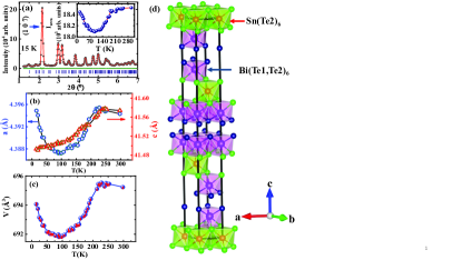
Analysis of the synchrotron diffraction patterns using Rietveld refinement indicates that the same structure is retained in the entire recorded temperature () range. Structural refinement at a representative temperature (15 K) is depicted in Fig. 1(a). The Rietveld refined coordinates are Sn (0,0,0), Te1 (0,0,0.13685(1)), Te2 (0,0,0.26758(8)), and Bi (0,0,0.42963(7)) with the refinement reliability parameters, (%) = 8.2, (%) = 4.15, and = 1.56. Inset of Fig. 1(a) depicts thermal variation of the integrated intensity (Iarea) of the (107) peak. The Iarea decreases with almost linearly until 170 K, below which it further decreases rapidly, following a significant increase below 100 K down to lowest recorded temperature. The lattice constant () and unit cell volume () follow a similar -dependence, see Fig. 1(b,c). The anomalous low- increase of is considerable as 0.33 % at 15 K with respect to the value at 100 K. Figure 1(d) shows the stacking of Sn(Te2)6 and Bi(Te1,Te2)6 octahedra along the -axis, as obtained from the refined atomic positions.
Figures 2(a) and 2(b) show a variation of resistivity () with the magnetic field () applied and to the [001] direction, respectively. Here, the subscript ‘’ represents same direction of the applied current and the recorded voltage, where the electrical connections are made on the (001) plane. For both the and components, the show typical metallic character down to 150 K, below which a semiconducting behavior is observed. A maximum in is noticed around 60 K, which is followed by a decreasing trend down to 2 K in both cases. The in the present system is similar to that observed in Bi2Se3 che09 ; but10 , Bi2Te3 kim12 , and Bi2Te2Se and Bi2-xSbxTe2S cai18 . for Bi2Se3 has been characterized by its dominant bulk contribution che09 ; but10 . On the other hand, the antisite disorder in Bi2Te3 was suggested to be responsible for low- semiconducting behavior. For Bi2Te2Se and Bi2-xSbxTe2S, surface and bulk contribution to were proposed to be independent, and giving rise to a semiconducting-like behavior in low T regime dominant by surface states cai18 . For SnBi2Te4, the value of lies in the range 0.3-0.8 m-cm, which is at least one order of magnitude lower than the reported results, pointing towards a more dominant metallic character in SnBi2Te4.
The magnetoresistance (MR), defined as [ - ]/, curves at selected are shown in the insets of Fig. 2(a) and 2(b) for the and components respectively, where lower and upper insets in both the panels display the low- ( 150 K) and high- curves, respectively. As evident from the upper inset of Fig. 2(a), nature of the curves at high- in the high- region ( K) are different from the low- MR curves. The details of the MR curves are shown in Figs. S2(a) and S2(b) of SM sup . The orbital contribution to MR in the nonmagnetic metals was explained by Kohler, known as the Kohler’s rule (KL) koh38 . The semi-classical KL has been tested for various systems viz., quasi-2D metal mck98 , graphite and bismuth kop06 , Weyl semimetal wan15 , topological semimetals jo17 ; dal21 . Kohler’s rule is verified for both the and components of MR, see Figs. S2(b) and S2(c) of SM sup . The MR curves for the component follow a single master curve for 15 K, above which they deviate and follow the KL until 150 K. The deviation from the master curve of KL was recently explained via a -dependent change in carrier densities xu21 , which is followed in our present system as well, as explained below. The rule is satisfied for the component of MR as well, but does not follow a single master curve.
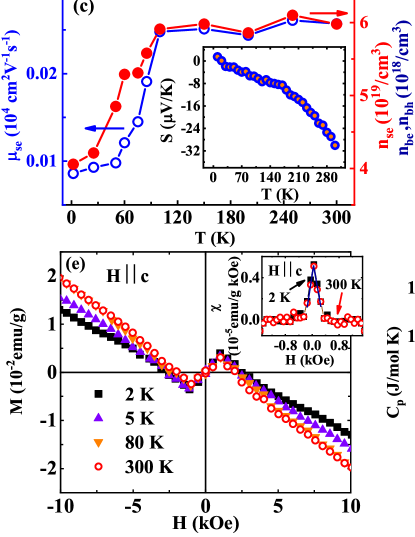
The mobilities and carrier densities are obtained from the -dependent Hall resistivity (), as shown in Fig. S2(e) of SM sup . Interestingly, conductivities () do not fit a two-band model hua15 ; dal21 , rather a three-band model par18 ; ant96 is required to correctly capture all the features. The expression for three-band model and satisfactory global fits (see Fig. S2(f) of SM) of are shown in SM sup . The three-band model suggests the two electron-type Fermi pockets and one hole-type Fermi pocket, implying coexistence of surface and bulk conductivities. The bulk conductivity is governed by the electron () and hole () mobilities. Let us denote , , and as the carrier densities of surface and bulk electrons, and bulk holes, respectively, while as the mobility of the surface electrons. As depicted in Fig. 2(c), and follow similar -dependence i.e. nearly -independent until 120 K, below which a sharp decrease is observed. Both parameters show a nearly -independent behavior at low-. The and are nearly -independent until 120 K (see Fig. 2(d)), below which they increase with decreasing and indicate a nearly -independent trend at low . The and are shown in the inset of Fig. 2(d), which are nearly -independent until 120 K, below which both of them show contrasting behavior. decreases, whereas increases below 120 K. The Inset of Fig. 2(c) displays the Seebeck coefficient () vs. , exhibiting a non-linear behavior, indicating the existence of more than one type of charge carrier. The value of is -30 V/K at 300 K, which indicates dominant electron conduction, consistent with the Hall measurement results.
Figure 2(e) shows the magnetization curves () at selected between 2 and 300 K, where is applied to [001]. The curves show a diamagnetic character over a wide -range except at low- (0.3 kOe), where a typical paramagnetic behavior is observed. The susceptibility () is obtained from the first-order derivative of the curve with respect to . The height of the peak in over the diamagnetic background remains almost the same at 2 and 300 K, as evident in the inset. The paramagnetic singularity at low- has been proposed due to the helical spin texture of 2D Dirac fermions on the surface, as also suggested for (Bi,Sb)2(Se,Te)3 zha14 , ZrTe5 par16 , and Bi1.5Sb0.5Te1.7Se1.3 dut17 .
To confirm the absence of any structural phase transition, -variation of the specific heat capacity was recorded in zero-field from 4 to 300 K, as shown in Fig. 2(f). The data does not show any anomaly over the recorded -region. The data in the intermediate temperature range does not fit well with either Debye or Einstein model. However, a trial with a combined Debye and Einstein model satisfactorily fits the experimental data using shang19 ; kumar22 ; chat20 ; ban18 ; das20 , . The combined Debye and Einstein model represent the acoustic and optical phonon-mode contributions tar03 . The best fit is shown by the solid curve in Fig. 2(f) with = 105.7 K, = 175.1 K, and = 0.59. The low- linear temperature coefficient of is found to be 32.1 mJ mol-1K-2 (obtained by subtracting the lattice contribution) which is comparable to the reported results for a TI phe14 .
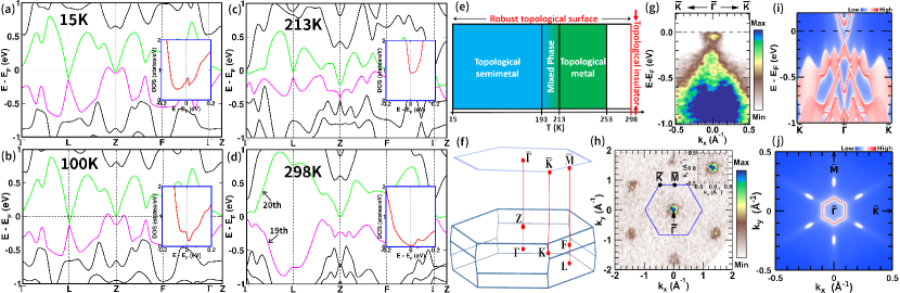
To better understand our experimental data, electronic band structures and density of states (DOS) of SnBi2Te4 were simulated using the experimental lattice parameters and Wyckoff positions (henceforth referred as ELEW) obtained at different . Computational details are given in SM sup . The results at a few representative (15 K, 100 K, 213 K, 298 K) are shown in Fig. 3(a-d) with the DOS near E shown in insets. For electronic structures at few other intermediate , we refer the reader to Fig. S3 of SM sup . At 15 K, one can notice the presence of a relatively moderate DOS with a small peak at E (see inset of Fig. 3(a)). This small peak remains upto 60 K which indirectly supports the increasing and hence metallic trend of in the range 260 K. Beyond 60 K, this peak begins to shift below E and slowly disappears (see inset of Fig. 3(b)). This again corroborates with the decreasing, and hence semiconducting trend of in the range 60150 K. At 213 K, it shows a relatively high DOS near E (see Fig. 3(c) inset), explaining an upturn and hence a weak metallic trend of in the range 150300 K, with a lower magnitude of than that seen in the 260 K range. Interestingly, at 298 K, there is almost vanishing DOS at/near E indicating a semiconducting bulk nature. Thus, the electronic DOS gives us a hint at a possible competition between semiconducting/semimetallic and metallic phases in our system. The origin of such diverse electronic phases is attributed to the sensitive changes in the internal atomic coordinates (Wyckoff positions) with . The lattice parameters of SnBi2Te4 at both 15 K and 298 K are very close to each other (within 0.2%) but their Wyckoff positions are very different. This leads to very different bulk band structures mediated by the impact on the bond lengths which in turn affects the hybridization between different atoms. This change in atomic coordinates does not stimulate any structural transition or symmetry-breaking. The band structures are especially sensitive to the position of Te2 atoms which are sandwiched between Sn and Bi atoms and hence helps in the formation of metallic octahedra around both Sn and Bi. Such sensitive dependence on ELEW has also been explored earlier in a different class of topological materials belonging to the same space group lin10 ; kuroda10 ; chang11 ; eremeev11 ; ohtsubo .
We further performed parity analysis of the filled bands to compute the invariants fu2007 at the representative . Other than 298 K, the electrons were partially filled up to the 20th band, while at 298 K, the 20th band shifts above E and the 19th band becomes the topmost filled band. From parity analysis, we obtain for SnBi2Te4 at all with the change in parity occurring either at or Z point in the bulk (see Fig. S4 of SM sup ). Hence, SnBi2Te4 is a strong TI, as reported earlier. Correspondingly, band inversion between Bi- and Te- orbitals is prominently visible along the Z direction at all (see Fig. S3 of SM). This guarantees the presence of topologically non-trivial surface states (TSS) at all due to the bulk-boundary correspondence. This is a remarkable result since it shows the robustness of the TSS and their insensitivity to in spite of the complicated hybridizations reflected in the bulk bands near E in the entire -range. Hence, we propose a schematic electronic phase diagram for SnBi2Te4, shown in Fig. 3(e). Due to scarce experimental structural data, the range 193 K 213 K is labelled ‘Mixed Phase’. The range 253 K 298 K is kept blank due to no experimental data. Further studies on SnBi2Te4 at different may help identify the nature of the crossover regions and whether these changes in the electronic structure are abrupt or gradual in nature.
To probe the surface states experimentally, ARPES measurements were done at 15 K. The results are shown in Figs. 3(g) and 3(h). A conical outline is clearly visible in Fig. 3(g) confirming the presence of a Dirac cone with the nodal point at -0.16 0.01 eV below E. The Fermi surface shown in Fig. 3(h) shows the isolated nature of the surface states with high local DOS at/around only. In ternary layered materials such as SnBi2Te4, surface relaxation plays an important role and can have significant effects on the surface band structure chang11 ; eremeev11 . Simulated surface band structure and Fermi surface of SnBi2Te4 using relaxed internal atomic coordinates are shown in Figs. 3(i) and 3(j). Simulations using relaxed coordinates at other yield similar results. The expected Dirac-like dispersion is seen around with the nodal point at -0.156 eV below E. The corresponding Fermi surface shows the well-known hexagonal warping of the Dirac cone away from the nodal point energy. There are 6 symmetric hole pockets around the cone originating from trivial surface states crossing E along the direction. The corresponding helical spin textures are shown in Fig. S5 of SM sup . The absence of hole pockets in ARPES data may be attributed to the use of soft X-rays which was not sufficient to resolve such finer details. For completeness, we have also simulated the surface dispersion using ELEWs at a few representative , as shown in Fig. S5 of SM sup . Helical TSS is observed in all of them which further highlights their robustness and the surface sensitivity, as discussed earlier. The above results also correspond well with the experimental signature of paramagnetic singularity obtained at both 2 K and 300 K (see inset of Fig. 2(c)) as mentioned earlier.
It is worth noting that the overall magnitude of is of the order of , which suggests dominant metallic type transport. This can now be attributed to the TSS since is also an order of magnitude higher than and (see Fig. 2(c) and 2(d)). Thus, one can assert that the overall transport is metal-like due to the TSS but the finer changes in with have a bulk origin. The Hall conductivities (see Fig. S2 of SM sup ) were fitted with a three-band model, indicating the presence of three types of charge carriers, which further aligns with the outcome of our simulated electronic structure analysis. Semimetals have both electrons and holes as carriers in the bulk. The presence of TSS below E provides electrons as carriers on the surface.
In summary, we present unconventional temperature mediated topological electronic phase transitions in SnBi2Te4. The system goes from a low- topological semimetallic phase to a high- (room temperature) topological insulator phase via an intermediate topological metal phase. Such unusual transition is intimately connected to the temperature dependent experimental lattice parameters, as demonstrated by our synchrotron based XRD data. The inherent nature of these phases are distinguished by ab-initio calculations done with the -dependent experimental lattice parameters. Our simulated results at 15 K match fairly well with transport and ARPES data. Magnetization measurements confirm the presence of a paramagnetic singularity in the entire -range (2300 K), which supports the robustness of topological surface states obtained from the simulations. The coexistence of such unconventional electronic phases in a single compound is not common and hence gives us a new avenue to explore the evolution of such phases via -mediated structural changes. References zhang ; wagner ; book1 ; sin ; hurd ; kuznet ; dal20_see ; ton66 ; hoh64 ; kre96 ; kre96r ; kre93 ; blo94 ; kre99 ; per96 ; grimme10 ; mar97 ; sou01 ; mar12 ; mos08 ; piz20 ; lee81 ; lee81r ; san85 ; wu18 have been cited in the SM sup .
Acknowledgements: Synchrotron based X-ray diffraction and photoemission studies were performed at the light source PETRA III of DESY, a member of the Helmholtz Association (HGF). Financial support (Proposal No. I-20200322 & I-20191102) by the Department of Science & Technology (Government of India) provided within the framework of the India@DESY collaboration is gratefully acknowledged. AA acknowledges DST- SERB (Grant No. CRG/2019/002050) for funding to support this research.
References
- (1) M. Z. Hasan, C. L. Kane, Rev. Mod. Phys. 82, 3045-3067 (2010).
- (2) S. M. Young, S. Zaheer, J. C. Y. Teo, C. L. Kane, E. J. Mele, and A. M. Rappe, Phys. Rev. Lett. 108, 140405 (2012).
- (3) S.-Y. Xu, C. Liu, S. K. Kushwaha, R. Sankar, J. W. Krizan, I. Belopolski, M. Neupane, G. Bian, N. Alidoust, T.-R. Chang, H.-T. Jeng, C.-Y. Huang, W.-F. Tsai, H. Lin, P. P. Shibayev, F.-C. Chou, R. J. Cava, and M. Z. Hasan, Science 347, 294 (2015).
- (4) B.-J. Yang, N. Nagaosa, Nat. Commun. 5, 4898 (2014).
- (5) A. C. Potter, I. Kimchi, A. Vishwanath, Nat. Commun. 5, 5161 (2014).
- (6) D. Hsieh, Y. Xia, L. Wray, D. Qian, A. Pal, J. H. Dil, J. Osterwalder, F. Meier, G. Bihlmayer, C. L. Kane, Y. S. Hor, R. J. Cava, and M. Z. Hasan, Science 323, 919 (2009).
- (7) D. Hsieh, L. Wray, D. Qian, Y. Xia, Y. Hor, R. Cava, and M. Hasan, arXiv:1001.1574 (unpublished).
- (8) A. A. Taskin and Y. Ando, Phys. Rev. B 80, 085303 (2009).
- (9) A. Taskin, K. Segawa, and Y. Ando, Phys. Rev. B 82, 121302(R) (2010).
- (10) Y. S. Hor, P. Roushan, H. Beidenkopf, J. Seo, D. Qu, J. G. Checkelsky, L. A. Wray, D. Hsieh, Y. Xia, S.-Y. Xu, D. Qian, M. Z. Hasan, N. P. Ong, A. Yazdani, and R. J. Cava Phys. Rev. B 81, 195203 (2010).
- (11) J. Analytis, J. Chu, Y. Chen, F. Corredor, R. McDonald, Z. Shen, and I. Fisher, Phys. Rev. B 81, 205407 (2010).
- (12) K. Eto, Z. Ren, A. A. Taskin, K. Segawa, and Y. Ando, Phys. Rev. B 81, 195309 (2010).
- (13) Y. Ran, Y. Zhang, and A. Vishwanath, Nat. Phys. 5, 298 (2009).
- (14) D. L. Bergman and G. Refael, Phys. Rev. B 82, 195417 (2010).
- (15) D. L. Bergman, Phys. Rev. Lett. 107, 176801 (2011).
- (16) C. Ortix, J. W. F. Venderbos, R. Hayn, and J. van den Brink, Phys. Rev. B 89, 121408(R) (2014).
- (17) Y. L. Chen, J. G. Analytis, J.-H. Chu, Z. K. Liu, S.-K. Mo, X. L. Qi, H. J. Zhang, D. H. Lu, X. Dai, Z. Fang, S. C. Zhang, I. R. Fisher, Z. Hussain, and Z.-X. Shen, Science 325, 178 (2009).
- (18) L. E. Shelimov, O. G. Karpinskii, P. P. Konstantinov, E. S. Avilov, M. A. Kretov, and V. Zemskov, Inorg. Mater. 40, 451 (2004).
- (19) L. Zhang and D. J. Singh, Phys. Rev. B 81, 245119 (2010).
- (20) M. Samanta, T. Ghosh, S. Chandra, and K. Biswas, J. Mater. Chem. A 8, 12226 (2020).
- (21) H. Zhang, L. Lu, and S. Mi, J. Mater. Chem. C 10, 854 (2022).
- (22) B. A. Kuropatwa, A. Assoud, and H. Kleinke, Z. Anorg. Allg. Chem. 639, 2411 (2013).
- (23) L. Pan, J. Li, D. Berardan, and N. Dragoe, J. Solid State Chem. 225, 168 (2015).
- (24) C. Lee, J. N. Kim, J.-Y. Tak, H. K. Cho, J. H. Shim, Y. S. Lim, and M.-H. Whangbo, AIP Advances 8, 115213 (2018).
- (25) G. R. Gurbanov and M. B. Adygezalov, Semiconductors 55, 943 (2021).
- (26) K. Kuroda, H. Miyahara, M. Ye, S. V. Eremeev, Yu. M. Koroteev, E. E. Krasovskii, E. V. Chulkov, S. Hiramoto, C. Moriyoshi, Y. Kuroiwa, K. Miyamoto, T. Okuda, M. Arita, K. Shimada, H. Namatame, M. Taniguchi, Y. Ueda, and A. Kimura, Phys. Rev. Lett. 108, 206803 (2012).
- (27) A. Marcinkova, J. K. Wang, C. Slavonic, A. H. Nevidomskyy, K. F. Kelly, Y. Filinchuk, and E. Morosan, Phys. Rev. B 88, 165128 (2013).
- (28) N. K. Singh, D. Rawat, D. Dey, A. Elsukova, Per O. Å. Persson, Per Eklund, A. Taraphder, and A. Soni, Phys. Rev. B 105, 045134 (2022).
- (29) Y. Li, C. Huang, G. Wang, J. Hu, S. Duan, C. Xu, Q. Lu, Q. Jing, W. Zhang, and D. Qian, Chin. Phys. B 30, 127901 (2021).
- (30) S. Fragkos, L. Baringthon, P. Tsipas, E. Xenogiannopoulou, P. Le Févre, P. Kumar, H. Okuno, N. Reyren, A. Lemaitre, G. Patriarche, J.-M. George, and A. Dimoulas, Phys. Rev. Mater. 5, 014203 (2021).
- (31) R. Vilaplana, J. Sans, F. Manjón, A. Andrada-Chacón, J. Sánchez-Benítez, C. Popescu, O. Gomis, A. Pereira, B. Garcíıa-Domene, P. Rodríguez-Hernández, A. Muoz, D. Daisenberger, and O. Oeckler, J. Alloys Compd. 685, 962 (2016).
- (32) Y.-C. Zou, Z.-G. Chen, E. Zhang, F. Kong, Y. Lu, L. Wang, J. Drennan, Z. Wang, F. Xiu, K. Cho, and J. Zou, Nano Research 11(2), 696–706 (2018).
- (33) K. Yang, W. Setyawan, S. Wang, M. B. Nardelli, and S. Curtarolo, Nat. Mater. 11, 614 (2012).
- (34) M. G. Vergniory, T. V. Menshchikova, I. V. Silkin, Yu. M. Koroteev, S. V. Eremeev, and E. V. Chulkov, Phys. Rev. B 92, 045134 (2015).
- (35) T. V. Menshchikova, S. V. Eremeev, Yu. M. Koroteev, V. M. Kuznetsov, and E. V. Chulkov, JETP Letters 93, 15 (2011).
- (36) K. Sun, Nat. Mater. 14, 262 (2015).
- (37) A. Y. Kuntsevich, M. A. Bryzgalov, V. A. Prudkoglyad, V. P. Martovitskii, Y. G. Selivanov, and E. G. Chizhevskii, New J. Phys. 20, 103022 (2018).
- (38) See Supplemental Materials in LINK.
- (39) J. G. Checkelsky, Y. S. Hor, M. H. Liu, D. X. Qu, R. J. Cava, and N. P. Ong, Phys. Rev. Lett. 103, 246601 (2009).
- (40) N. P. Butch, K. Kirshenbaum, P. Syers, A. B. Sushkov, G. S. Jenkins, H. D. Drew, and J. Paglione, Phys. Rev. B 81, 241301(R) (2010).
- (41) H.-J. Kim, K.-S. Kim, M. D. Kim, S. J. Lee, J. W. Han, A. Ohnishi, M. Kitaura, M. Sasaki, A. Kondo, and K. Kindo, J. Phys. Conf. Ser. 400, 042033 (2012).
- (42) S. Cai, J. Guo, V. A. Sidorov, Y. Zhou, H. Wang, G. Lin, X. Li, Y. Li, K. Yang, A. Li, Q. Wu, J. Hu, S. K. Kushwaha, R. J. Cava, and L. Sun, Npj Quantum. Materials 3, 62 (2018).
- (43) M. Kohler, Ann. Phys. (Berlin) 424, 211 (1938).
- (44) R. H. McKenzie, J. S. Qualls, S. Y. Han, and J. S. Brooks, Phys. Rev. B 57, 11854 (1998).
- (45) Y. Kopelevich, J. C. Medina Pantoja, R. R. da Silva, and S. Moehlecke, Phys. Rev. B 73, 165128 (2006).
- (46) Y. L. Wang, L. R. Thoutam, Z. L. Xiao, J. Hu, S. Das, Z. Q. Mao, J. Wei, R. Divan, A. Luican-Mayer, G. W. Crabtree, and W. K. Kwok, Phys. Rev. B 92, 180402(R) (2015).
- (47) N. H. Jo, Y. Wu, L.-L. Wang, P. P. Orth, S. S. Downing, S. Manni, D. Mou, D. D. Johnson, A. Kaminski, S. L. Budko, and P. C. Canfield, Phys. Rev. B 96, 165145 (2017).
- (48) T. K. Dalui, P. K. Ghose, S. Majumdar, S. K. Mahatha, F. Diekmann, K. Rossnagel, R. Tomar, S. Chakraverty, A. Berlie, and S. Giri, Phys. Rev. B 103, 064428 (2021).
- (49) J. Xu, F. Han, T.-T. Wang, L. R. Thoutam, S. E. Pate, M. Li, X. Zhang, Y.-L. Wang, R. Fotovat, U. Welp, X. Zhou, W.-K. Kwok, D. Y. Chung, M. G. Kanatzidis, and Z.-L. Xiao, Phys. Rev. X 11, 041029 (2021).
- (50) X. Huang, L. Zhao, Y. Long, P. Wang, D. Chen, Z. Yang, H. Liang, M. Xue, H. Weng, Z. Fang, X. Dai, and G. Chen, Phys. Rev. X 5, 031023 (2015).
- (51) A. Pariari, R. Singha, S. Roy, B. Satpati and P. Mandal, Sci. Rep. 8, 10527 (2018).
- (52) J. Antoszewski and L. Faraone, J. Appl. Phys. 80, 3881 (1996).
- (53) L. Zhao, H. Deng, I. Korzhovska, Z. Chen, M. Konczykowski, A. Hruban, V. Oganesyan and L. K. Elbaum, Nat. Mat. 13, 580 (2014).
- (54) A. Pariari and P. Mandal Sci. Rep. 7, 40327 (2016).
- (55) P. Dutta, A. Pariari and P. Mandal, Sci. Rep. 7, 4883 (2017).
- (56) T. Shang, A. Amon, D. Kasinathan, W. Xie, M. Bobnar, Y. Chen, A. Wang, M. Shi, M. Medarde, H. Q. Yuan and T. Shiroka New J. Phys. 21, 073034 (2019).
- (57) R. Kumar and A. Sundaresan, Phys. Rev. B 106, 134423 (2022).
- (58) S. Chatterjee, P. Dutta, S. Giri, S. Majumdar, S. Sadhukhan, S. Kanungo, S. Chatterjee, M. M. Patidar, G. S. Okram, and V. Ganesan, Phys. Rev. B 102, 214443 (2020).
- (59) A. Banerjee, J. Sannigrahi, S. Giri, and S. Majumdar, Phys. Rev. B 98, 104414 (2018).
- (60) M. Das, P. Sarkar, and P. Mandal Phys. Rev. B 101, 144433 (2020).
- (61) A. Tari, The Specific Heat of Matter at Low Temperatures (London: Imperial College Press, 2003).
- (62) W.A. Phelan, S.M. Koohpayeh, P. Cottingham, J.W. Freeland, J.C. Leiner, C.L. Broholm, and T.M. McQueen, Phys. Rev. X 4, 031012 (2014).
- (63) H. Lin, R. S. Markiewicz, L. A. Wray, L. Fu, M. Z. Hasan, and A. Bansil, Phys. Rev. Lett. 105, 036404 (2010).
- (64) K. Kuroda, M. Ye, A. Kimura, S. V. Eremeev, E. E. Krasovskii, E. V. Chulkov, Y. Ueda, K. Miyamoto, T. Okuda, K. Shimada, H. Namatame, and M. Taniguchi, Phys. Rev. Lett. 105, 146801 (2010).
- (65) Jiwon Chang, Leonard F. Register, Sanjay K. Banerjee, and Bhagawan Sahu, Phys. Rev. B 83, 235108 (2011)
- (66) S. V. Eremeev, G. Bihlmayer, M. Vergniory, Yu. M. Koroteev, T. V. Menshchikova, J. Henk, A. Ernst, and E. V. Chulkov, Phys. Rev. B 83, 205129 (2011).
- (67) Y. Ohtsubo, Y. Yamashita, J. Kishi, S. Ideta, K. Tanaka, H. Yamane, J. E. Rault, P. Le Fèvre, F. Bertran, and S. Kimura, J. Phys. D: Appl. Phys. 52, 254002 (2019).
- (68) L. Fu and C. L. Kane, Phys. Rev. B 76, 045302 (2007).
- (69) G. Zhang, H. Qin, J. Teng, J. Guo, Q. Guo, X. Dai, Z. Fang, and K. Wu, Appl. Phys. Lett. 95, 053114 (2009).
- (70) C. D. Wagner, J. Electron Spectrosc. Relat. Phenom. 32, 99 (1983).
- (71) J. M. Ziman, in Electrons and Phonons: The Theory of Transport Phenomena in Solids, Classics Series (Oxford University Press, New York, 2001).
- (72) R. Singha, A. Pariari, B. Satpati and P. Mandal Phys. Rev. B 96, 245138 (2017).
- (73) C. M. Hurd, The Hall Effect in Metals and Alloys. (Plenum, New York, 1972).
- (74) L.A. Kuznetsova, V.L. Kuznetsov, D.M. Rowe, Journal of Physics and Chemistry of Solids 61, 1269–1274 (2000).
- (75) T. K. Dalui, P. K. Ghose, S. Majumdar, and S. Giri, J. Phys.: Condens. Matter 32, 435601 (2020).
- (76) B. Y. Tong and L. J. Sham, Phys. Rev. 144, (1966).
- (77) P. Hohenberg and W. Kohn, Phys. Rev. 136, B864 (1964).
- (78) G. Kresse and J. Furthmüller, Phys. Rev. B 54, 11169 (1996).
- (79) G. Kresse and J. Furthmüller, J. Comput. Mater. Sci. 6, 15 (1996).
- (80) G. Kresse and J. Hafner, Phys. Rev. B 47, 558(R) (1993).
- (81) P. E. Blöchl, Phys. Rev. B 50, 17953 (1994).
- (82) G. Kresse and D. Joubert, Phys. Rev. B 59, 1758 (1999).
- (83) J. P. Perdew, K. Burke, and M. Ernzerhof, Phys. Rev. Lett. 77, 3865 (1996).
- (84) S. Grimme, J. Antony, S. Ehrlich, and S. Krieg, J. Chem. Phys. 132, 154104 (2010).
- (85) N. Marzari and D. Vanderbilt, Phys. Rev. B 56, 12847 (1997).
- (86) I. Souza, N. Marzari, and D. Vanderbilt, Phys. Rev. B 65, 035109 (2001).
- (87) N. Marzari, A. A. Mostofi, J. R. Yates, I. Souza, and D. Vanderbilt, Rev. Mod. Phys. 84, 1419 (2012).
- (88) A. A. Mostofi, J. R. Yates, Y.-S. Lee, I. Souza, D. Vanderbilt, and N. Marzari, Comput. Phys. Commun. 178, 685 (2008).
- (89) G. Pizzi, et al. J. Phys.: Condens. Matter 32, 165902 (2020).
- (90) D. H. Lee and J. D. Joannopoulos, Phys. Rev. B 23, 4988 (1981).
- (91) D. H. Lee and J. D. Joannopoulos, Phys. Rev. B 23, 4997 (1981).
- (92) M. P. Lopez Sancho, J. M. Lopez Sancho, J. M. L. Sancho, and J. Rubio, J. Phys. F: Met. Phys. 15, 851 (1985).
- (93) Q. S. Wu, S. N. Zhang, H.-F. Song, M. Troyer, and A. A. Soluyanov, Comput. Phys. Commun. 224, 405 (2018).