Moiré Superstructures in Marginally-Twisted NbSe2 Bilayers
Abstract
The creation of moiré superlattices in twisted bilayers of two-dimensional crystals has been utilised to engineer quantum material properties in graphene and transition metal dichalcogenide (TMD) semiconductors. Here, we examine the structural relaxation and electronic properties in small-angle twisted bilayers of metallic NbSe2. Reconstruction appears to be particularly strong for misalignment angles and for parallel (P) and antiparallel (AP) orientation of monolayers’ unit cells, respectively. Multiscale modelling reveals the formation of domains and domain walls with distinct stacking, for which density functional theory (DFT) calculations are used to map the shape of the bilayer Fermi surface and the relative phase of the charge density wave (CDW) order in adjacent layers. We find a significant modulation of interlayer coupling across the moiré superstructure and the existence of preferred interlayer orientations of the CDW phase, necessitating the nucleation of CDW discommensurations at superlattice domain walls.
I Introduction
Introduction — The field of twistronics, where a relative twist is applied between adjacent layers in two-dimensional crystalline structures, has recently emerged as a promising method to control electronic [1, 2] and structural [3, 4, 5, 6, 7, 8, 9, 10, 11, 12] properties. For example, in semiconducting TMDs, with chemical formula MX2 (M = Mo, W; X = S, Se), it has recently been established that the moiré pattern in twisted bilayers undergoes significant reconstruction [4, 5, 6, 13] at marginal (i.e. sufficiently small) twist angles.
The niobium (or tantalum) atoms of metallic TMDs host one fewer d-electron in the valence shell. The chemical potential then lies in the valence band, in contrast to semiconducting TMDs, allowing superconducting and charge-density wave (CDW) phases in monolayer and bulk [14, 15, 16, 17, 18, 19]. Here, interlayer effects are also found to be important, moderating the critical temperatures of the superconducting [20, 21] and CDW [22, 23] transitions, enabling van der Waals Josephson junctions through interlayer twisting [24, 25] and leading to spatial variation of the Gibbs free energy of hydrogen absorption [26]. Despite these fascinating properties, there have been no detailed theoretical studies of the structural relaxation of twisted bilayers of metallic TMDs, and the consequent effect of stacking on electronic properties. Here we address these questions for twisted bilayers of NbSe2 using ab-initio density functional theory (DFT) modelling combined with multiscale analysis of lattice relaxation.
Ab-initio analysis of adhesion energy — DFT calculations were performed as implemented in the Quantum ESPRESSO code [27, 28]. Core electrons were approximated using Vanderbilt ultrasoft pseudopotentials [29] under the generalized gradient approximation (GGA), as parameterised by Perdew, Burke and Ernzerhof [30]. A plane-wave cut-off of Ry and charge density cut-off of Ry were applied. A Monkhorst-Pack k-point grid of dimensions [31] and Fermi-Dirac smearing of width eV is applied to aid convergence. Interlayer dispersion is implemented through the optB88-vdW functional [32, 33, 34, 35]. Band structure calculations were performed using Ry and a k-point grid. In both band structure & adhesion parameterisation calculations, we fix the in-plane lattice constant to the bulk value.
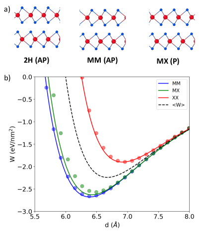
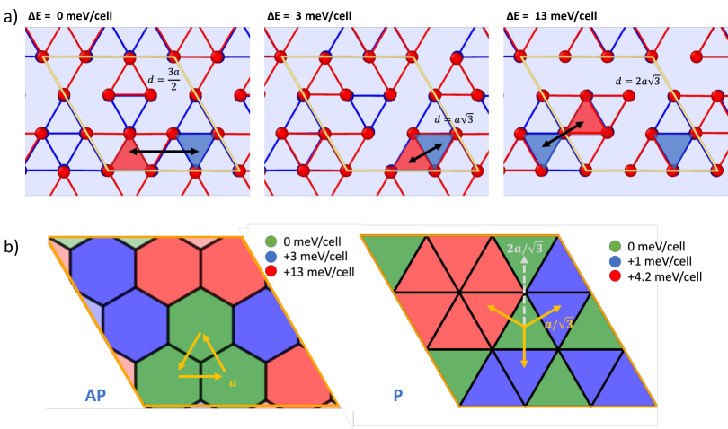
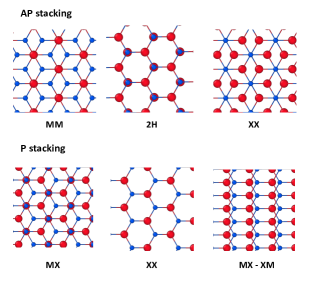
To assess the preferred stacking order, bilayers of NbSe2 were structurally relaxed in a variety of stacking configurations illustrated by sketches in Fig. 1a. Bilayer structures are divided into two classes: anti-parallel (AP), where a 180o rotation of the top layer restores centrosymmetry, which is absent in a monolayer, and parallel (P) where monolayers have the same orientation and centrosymmetry is absent. Comparison of different stackings shows that the lowest-energy stacking polymorph is the metal-overlapping, MM (also called 2Ha [36, 37]) configuration (see Fig. 1b), for which DFT bulk lattice constants, a = 3.45 and c = 12.74 [38], and elastic moduli (see Supplemental Information (SI) section S2), are all found to be in good agreement with available experimental values [38, 39, 40]. 2H-stacking, which is preferred for semiconducting TMDs, is reasonably close in energy. While it has been found with a smaller areal density in CVD-grown NbSe2 bilayers [41], it is a metastable state, whereas the MM configuration is most common and thermodynamically stable. We note that the bulk structure of NbSe2 has frequently been referred to (and sometimes even modelled) as 2H stacking [42, 43, 44, 45], therefore to avoid confusion, below we employ nomenclature of relevant stacking configurations as shown in Fig. 1.
In twisted bilayers, moiré superlattice reconstruction is fully determined by the stacking-dependent variation of adhesion energy between the constituent layers. Following the approach of Ref. [46] we employ an interpolation formula to fit the adhesion energy as a function of local disregistry, . This is parameterised in a coordinate system where XX stacking corresponds to zero displacement, i.e. , and interlayer distance :
| (1) | ||||
Here, is stacking-averaged adhesion energy, characterising long-distance van der Waals attraction between the layers (), and short-distance repulsion (), are reciprocal lattice vectors and , , are fit parameters. The phases, and distinguish P and AP unit cell orientations, reflecting the symmetry of these alignments.
Fitting to DFT results leads to optimal interlayer distances nm and nm for configuration-averaged and ground (MM) stackings, respectively. Expanding Eq. (1) around for , (, eV/nm4), allows us to estimate the frequency of the layer breathing mode in MM-stacked NbSe2 bilayers as follows: cm-1 ( meV) Here, and are mass and area of NbSe2 monolayer unit cell, respectively. The computed value is in a good agreement with the experimental value cm-1 [47] , which validates the DFT-fitted shape of the adhesion energy (1) around .
Lattice reconstruction in twisted NbSe2 bilayers is modelled using a multiscale approach implemented earlier in Ref. [46] for the analysis of semiconducting TMDs. This incorporates the microscopic expression for adhesion energy (1) and elasticity theory applied to the mesoscale strains across a long-period moiré superlattice, which reduces to minimization of total (adhesion and elastic) energy over the moiré supercell. In the elastic energy, characterised by elastic moduli and , we take into account only in-plane strains in top (t) and bottom (b) layers, , neglecting minor bending energies of layers (see SM in [46]) due to adjustment of local optimal interlayer distance with corresponding stacking across the moiré superlattice. To find the latter, we expand around its extremum (), exponential functions in (1) up to linear order in , and, then, minimise the resulting expression as a function of , to obtain an expression for the optimal interlayer distance for every stacking, . Here, , where the first term describes contribution of geometrical twist between the layers, and in-plane displacements, , responsible for local deformations in t/b-layer, are found from minimisation to the total energy.
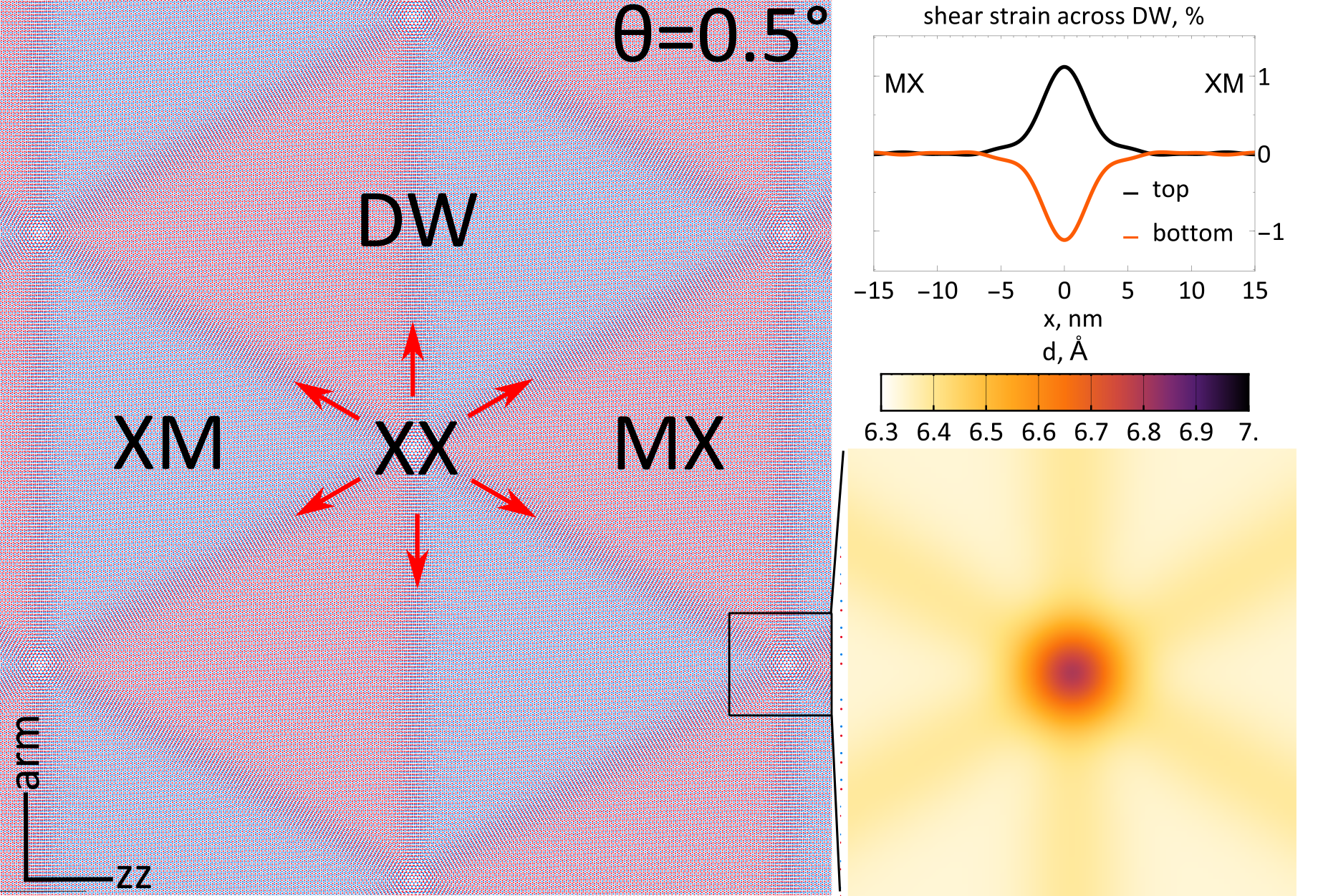
In Fig. 2 we display the reconstructed moiré superlattice resulting from minimisation of total energy in twisted NbSe2 bilayers. Similarly to semiconducting TMDs, at 111Value of critical angles result from equality of gain from formation of domains to the costs of domain wall network. this results in the formation of arrays of triangular domains with rhombohedral stacking (XM and MX), separated by a domain wall network. Each domain wall in the network is a partial screw dislocation with dominating shear strain and a Burgers vector length , shown by red arrows for several DWs merging into a DW network node. The magnitude of shear strain reaches 1% in the middle of domain wall, see Fig. 2, inset.
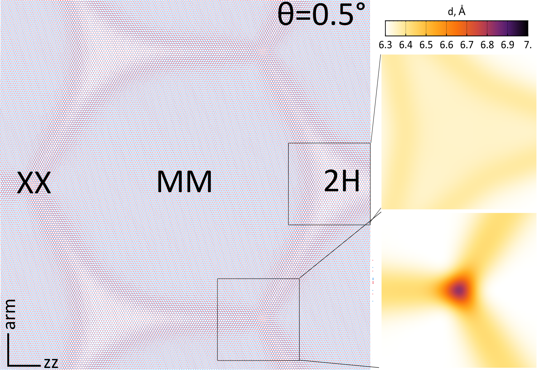
For AP-NbSe2 bilayers with , Fig. 3, lattice reconstruction leads to the expansion of the lowest energy MM domains, and the formation of a hexagonal superlattice domain wall network. The other high-symmetry (2H and XX) stackings occupy corners of the domains, linked by perfect screw dislocations, characterized by a stacking shift of a single translation vector along zigzag axes. We note that the critical angles, are slightly higher than those for semiconducting TMDs [46] because of the softer NbSe2 lattice.
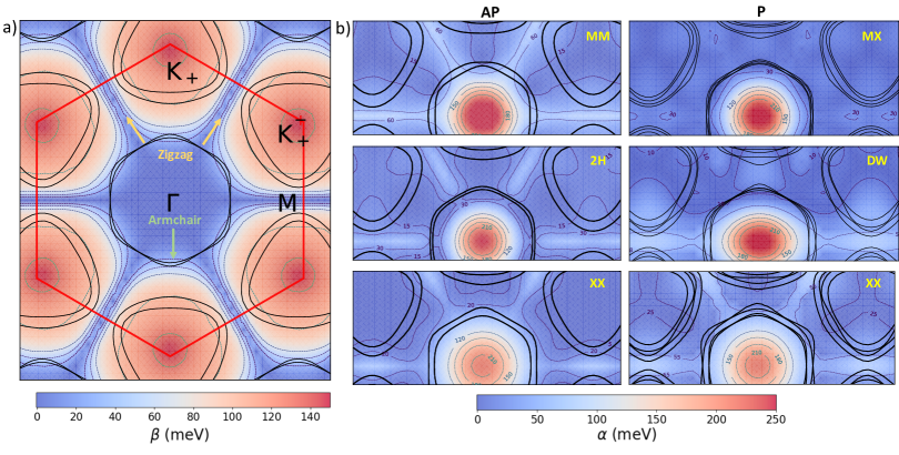
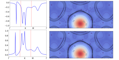
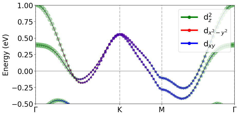
Electronic structure — The Fermi surface of an NbSe2 monolayer is shown in Fig. 4a. There are three distinct hole pockets across the Brillouin zone: one -centred pocket and a pair of triangular K± pockets. The dispersion around each pocket () is
| (2) |
where is Bloch state momentum relative to the pocket centre, is effective mass, parameters account for trigonal and hexagonal warping, is a Pauli matrix operating on spin, arctan [49], and is the energy difference between the band edge and the Fermi level. The shape of the metallic band is overall extremely similar to the conduction band in semiconducting TMDs, with similar effective masses and a high degree of trigonal warping around the K-pockets (see Table 1) [16]. Significant Ising spin-orbit coupling (SOC) is evident across the BZ, with splitting . A map of across the entire BZ is displayed in Fig. 4a, with a maximum value of 78 meV deep in the K± pockets. In the -pocket SOC vanishes along -M lines, , while it is approximately constant, in the pockets [50].
| (eV) | (eVÅ3) | (meV) | ||
|---|---|---|---|---|
| 0.51 [0.58] | -2.52 [-1.92] | 1.29 [0.37] | 35 [35] | |
| K | 0.31 [0.53] | -1.40 [-0.61] | 3.41 [13.50] | 55 [67] |
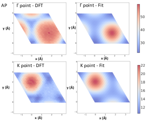
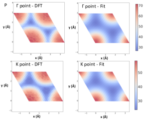
Stacking modulation of interlayer hybridization results in variation of the electronic Fermi surface around each pocket. To quantify this, we relate DFT-calculated energy eigenvalues across the entire Brillouin zone (BZ) to a momentum-dependent hybridization parameter , assuming a simple layer-hybridized wavefunction, , with energies, , where are monolayer energy eigenvalues. [51]
Plots of this parameter calculated across the BZ are overlaid with the DFT-calculated Fermi surface in Fig. 4b. We observe that in centrosymmetric AP configurations, interlayer hybridization leads to a pair of spin-layer locked, layer-hybridized bands which cross the Fermi level in all stacking configurations. In contrast, broken centrosymmetry of the P-bilayers leads to four Fermi lines, which are essentially a pair of layer-hybridized copies of the monolayer bands. DFT calculations in mirror-reflected supercells also demonstrate the presence of a ferroelectric charge transfer, resulting in 11 meV potential energy drop between the layers (see SI section S3), which is notably smaller than for semiconducting TMDs [52]. We note that this charge transfer in principle allows for a layer-dependent potential contribution to interlayer band splitting of P-bilayers, however, explicit incorporation of this term does not have a significant effect on interlayer hybridization due to the small degree of charge transfer between the layers (see comparison between Fermi surface fitting with and without an explicit layer-polarization term, SI section S4).
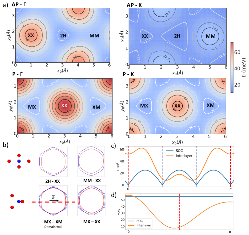
In both bilayer orientations, there is a substantial six/three-fold modulation of the hybridization parameter around the /K± pockets, as shown in Fig. 4b (see also SI section S5). This modulation is proportional to the out-of-plane -orbital component, leading to maxima along the -M and K-M lines around each pocket. The resulting interlayer hybridization, and the associated shape of the Fermi lines, is moderated by the interlayer coordination of Nb atoms. Consequently, there are also distinct modulations of the interlayer hybridization at domain walls, which is evident as a two-fold ”squeezing”, of both the and K-pockets, along distinguished directions of the Brillouin zone for the intermediate stacking configurations occurring at domain walls (see Fig. 4b, P-DW). For example, at the domain walls of a P-oriented moiré we find that there is significantly stronger hybridization of -pocket electrons with crystal momenta parallel to the dislocation line compared to the perpendicular direction, while the opposite is the case for the -pocket. A comparison of the degree of asymmetric warping, and the corresponding positions of Nb atoms in both layers, is shown in Fig. 5b for various intermediate stacking configurations of P and AP bilayers, which demonstrates qualitatively similar distortion between the two bilayers as a function of Nb-interlayer offset. Furthermore we note that, in both pockets, the degree of interlayer coupling can be lifted below or above that of the spin-orbit term, depending on pocket index and crystal momentum. (see Fig. 5c,d).
Using DFT data, we quantify effective interlayer hopping around each pocket by introducing an extra index which acts in layer space. This is encoded in a bilayer Hamiltonian,
| (3) | ||||
where / are electron creation/annihilation operators, is pocket index, is Bloch state momentum relative to the pocket centre, and are spin and layer indices. are Pauli matrices operating on the layer index, where the parameter a = for a AP, P bilayers respectively, and is the strength of hybridization around the corresponding pocket, where modulation is accounted for using appropriate periodic terms in . The hybridization term then takes the form,
| (4) |
where is the average hybridization around pocket. We find that hybridization is approximately constant for momenta , with angular variation incorporated via periodic terms. Further details of these terms in high-symmetry stackings are given in SI sections S6 and S7.
To facilitate simple comparison between different domains in the moiré superstructure, we analyse the average interlayer hopping, (the first term in Eq. 4), at each pocket as a function of interlayer disregistry. We numerically extract this parameter from DFT calculations by averaging interlayer splitting around each pocket along the high-symmetry directions (-M, -K, K-M, K-). This procedure was repeated for relaxed bilayers with different interlayer offsets, and the extracted value of was found to fit to an expansion using only the first star of reciprocal lattice vectors with reasonable accuracy (see SI section S8 and S9). Fig. 5a shows this expansion for both pockets in AP- and P-bilayers.
Interestingly, we find distinct variation of interlayer hybridization between the and K pockets in AP bilayers. For the former, which is most sensitive to the interlayer distance between Se atoms, it is maximal at XX corners, while interlayer hybridization at the K-pocket is strongest inside the lowest-energy MM domains. Interactions are weakest at the 2H corners for both pockets. An opposite trend was found for the moiré of a P-bilayer. In this case, the interlayer separation of chalcogen atoms is rather larger within domains due to trigonal interlayer coordination and there are correspondingly weaker interlayer interactions, which becomes larger at corners and domain walls where the interlayer Se distance is reduced. The overall variation is qualitatively similar at both pockets.
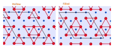
CDW Modulation — Lastly, we examine the ability of the reconstructed moiré superlattice to impact the relative phase of the CDW distortion in adjacent layers, as a function of the interlayer disregistry. CDW order in NbSe2 monolayers induces a reconstruction [53, 54, 20, 55, 56]. In a monolayer, we find two low energy triangular reconstructions of the lattice [57], which are characterised by one of two structural distortions, classified as ”Hollow” or ”Filled”, based on the distortion pattern of atoms in the Nb sublattice [58] (see SI section 10), and that the Hollow phase has lowest overall energy of the two.
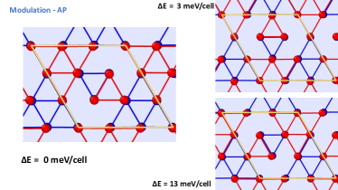
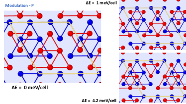
Both monolayer reconstructions are then used to create bilayer cells with different interlayer offsets of the CDW phase between the layers. The difference in DFT total energy between the normal (no reconstruction) and Hollow CDW phase on both layers, , is extracted to quantify the realtive strength of the CDW phase between different structures. In agreement with the monolayer case, we find that structures with the Hollow reconstruction on both layers are lowest in energy. We then calculate the relative strength of the CDW distortion at each of the 18 MX/XM (P) and 9 MM (AP) possible stacking configurations of the CDW in adjacent reconstructed layers. Fig. 6a shows these three unique structural configurations in the AP case, where only the Nb-sublattice is shown to improve clarity (see SI section 10 for additional figures of the monolayer CDW reconstructions, and the different interlayer configurartions of these structures considered in this work.)
We observe a notable trend in this energy difference with interlayer disregistry, shown in the bottom left (right) of Fig. 6b for the AP (P) bilayer. While it is possible to reach another low energy mutual orientation of the two CDW distortions in each layer via a full dislocation in the AP bilayer, this is not possible for P bilayers, where shifting by a partial dislocation always leads to a higher energy configuration. In a moiré superlattice, this suggests that the CDW order in adjacent layers will lock-in inside a domain. Glide of the lattice by a partial or full screw dislocation across domain boundaries will rigidly shift the relative orientation of the CDW on each layer, and, in order to attain a low-energy interlayer configuration, CDW discommensurations should nucleate at moiré dislocation boundaries [59, 60], leading to CDW triplet domains in an AP-moiré [61] and isolated CDW domains in a P-moiré.
In conclusion, multiscale relaxation and electronic structure calculations were performed on twisted bilayer NbSe2. Compared to semiconducting TMDs, monolayer NbSe2 is relatively soft, and significant relaxation begins at slightly larger twist angles. The resulting domain structure for AP-bilayers has hexagonal MM stacking domains with domain walls featuring XX stacking and seeds of 2H stacking in the alternating corners. The Fermi surface undergoes significant modulation across the moiré, with variation of the interlayer coupling at the K points on the order of 10-20 meV (25-55 meV) between different domains for an AP(P)-bilayer. Notably, there is significant anisotropy in the interlayer coupling is observed along domain walls. For AP-bilayers the interlayer coupling of metallic bands is strongest inside domains, in contrast to our finding regarding P-bilayers. In P-bilayers, the triangular MX/XM domains have smaller interlayer coupling of electron bands than along the triangular domain wall network.
A further observation arising from this work is that discommensurations [60] of the CDW phase should occur due to the rigid displacement of the relative orientation of the CDW in each layer which occurs at superlattice domain walls. CDW discommensurations are known to enhance the superconducting order in TiSe2 [62, 63, 64]. This suggests a promising application for moiré superlattices in metallic TMDs systems as a method to control the CDW, and potentially, other order parameters. The potential for distinct modulation of interlayer hopping at each pocket, in addition to control of the CDW phase, along with anisotropic hopping at dislocation boundaries, suggests that marginally-twisted NbSe2 would be an interesting test system to further probe interlayer effects on correlated superconducting and CDW phases of the metallic TMDs [20].
Finally, we remark on possible implications of our results for Ising superconductivity in marginally-twisted bilayers. At small angles, the interlayer coupling in both pockets across a significant area of the moiré supercell is of a similar magnitude to the MM bilayer, for both twisted AP and P bilayers. In multilayer NbSe2 [20] both the critical temperature, , and in-plane magnetic field of the superconducting transition show a significant dependence on the number of layers, suggesting the importance of interlayer electronic effects to the magnitude and form of the superconducting gap. If the breaking of spin-layer locking through increased interlayer hopping is the active mechanism in determining the superconducting transition temperature as a function of layer number, this suggests that the significant modulation of interlayer hopping by the moiré superstructure could be utilised to engineer superconductivity in specific domains of the superlattice. In an applied field, superconductivity would preferentially persist in regions of the moiré with smaller interlayer coupling, which are MX/XM domains (P-bilayer), or domain walls and corners (AP-bilayer).
Acknowledgements. This work was supported by EC-FET European Graphene Flagship Core3 Project, EC-FET Quantum Flagship Project 2D-SIPC, EPSRC grants EP/S030719/1 and EP/V007033/1, and the Lloyd Register Foundation Nanotechnology Grant.
References
- Sung et al. [2020] J. Sung, Y. Zhou, G. Scuri, V. Zólyomi, T. I. Andersen, H. Yoo, D. S. Wild, A. Y. Joe, R. J. Gelly, H. Heo, S. J. Magorrian, D. Bérubé, A. M. M. Valdivia, T. Taniguchi, K. Watanabe, M. D. Lukin, P. Kim, V. I. Fal’ko, and H. Park, Broken mirror symmetry in excitonic response of reconstructed domains in twisted MoSe2/MoSe2 bilayers, Nature Nanotechnology 15, 750 (2020).
- Chen et al. [2022] D. Chen, Z. Lian, X. Huang, Y. Su, M. Rashetnia, L. Ma, L. Yan, M. Blei, L. Xiang, T. Taniguchi, K. Watanabe, S. Tongay, D. Smirnov, Z. Wang, C. Zhang, Y.-T. Cui, and S.-F. Shi, Excitonic Insulator in a Heterojunction Moiré Superlattice, Nature Physics 18, 1171 (2022).
- Yoo et al. [2019] H. Yoo, R. Engelke, S. Carr, S. Fang, K. Zhang, P. Cazeaux, S. H. Sung, R. Hovden, A. W. Tsen, T. Taniguchi, and et al, Atomic and electronic reconstruction at the van der Waals interface in twisted bilayer graphene, Nature materials 18, 448 (2019).
- Weston et al. [2020] A. Weston, Y. Zou, V. Enaldiev, A. Summerfield, N. Clark, V. Zólyomi, A. Graham, C. Yelgel, S. Magorrian, M. Zhou, J. Zultak, D. Hopkinson, A. Barinov, T. H. Bointon, A. Kretinin, N. R. Wilson, P. H. Beton, V. I. Fal’ko, S. J. Haigh, and R. Gorbachev, Atomic reconstruction in twisted bilayers of transition metal dichalcogenides, Nature Nanotechnology 15, 592 (2020).
- Rosenberger et al. [2020] M. R. Rosenberger, H.-J. Chuang, M. Phillips, V. P. Oleshko, K. M. McCreary, S. V. Sivaram, C. S. Hellberg, and B. T. Jonker, Twist angle-dependent atomic reconstruction and moiré patterns in transition metal dichalcogenide heterostructures, ACS Nano 14, 4550 (2020).
- Halbertal et al. [2021] D. Halbertal, N. R. Finney, S. S. Sunku, A. Kerelsky, C. Rubio-Verdú, S. Shabani, L. Xian, S. Carr, S. Chen, C. Zhang, L. Wang, D. Gonzalez-Acevedo, A. S. McLeod, D. Rhodes, K. Watanabe, T. Taniguchi, E. Kaxiras, C. R. Dean, J. C. Hone, A. N. Pasupathy, D. M. Kennes, A. Rubio, and D. N. Basov, Moiré metrology of energy landscapes in van der waals heterostructures, Nature Communications 12, 242 (2021).
- McGilly et al. [2020] L. J. McGilly, A. Kerelsky, N. R. Finney, K. Shapovalov, E.-M. Shih, A. Ghiotto, Y. Zeng, S. L. Moore, W. Wu, Y. Bai, K. Watanabe, T. Taniguchi, M. Stengel, L. Zhou, J. Hone, X. Zhu, D. N. Basov, C. Dean, C. E. Dreyer, and A. N. Pasupathy, Visualization of moiré superlattices, Nature Nanotechnology 15, 580 (2020).
- Shabani et al. [2021] S. Shabani, D. Halbertal, W. Wu, M. Chen, S. Liu, J. Hone, W. Yao, D. N. Basov, X. Zhu, and A. N. Pasupathy, Deep moiré potentials in twisted transition metal dichalcogenide bilayers, Nature Physics 17, 720 (2021).
- Edelberg et al. [2020] D. Edelberg, H. Kumar, V. Shenoy, H. Ochoa, and A. N. Pasupathy, Tunable strain soliton networks confine electrons in van der waals materials, Nature Physics 16, 1097 (2020).
- Engelke et al. [2022] R. Engelke, H. Yoo, S. Carr, K. Xu, P. Cazeaux, R. Allen, A. M. Valdivia, M. Luskin, E. Kaxiras, M. Kim, and et al, Non-abelian topological defects and strain mapping in 2d moir’e materials, arXiv:2207.05276 (2022).
- Van Winkle et al. [2022] M. Van Winkle, I. M. Craig, S. Carr, M. Dandu, K. C. Bustillo, J. Ciston, C. Ophus, T. Taniguchi, K. Watanabe, A. Raja, S. M. Griffin, and D. K. Bediako, Quantitative imaging of intrinsic and extrinsic strain in transition metal dichalcogenide moiré bilayers (2022).
- Kazmierczak et al. [2021] N. P. Kazmierczak, M. V. Winkle, C. Ophus, K. C. Bustillo, S. Carr, H. G. Brown, J. Ciston, T. Taniguchi, K. Watanabe, and D. K. Bediako, Strain fields in twisted bilayer graphene, Nature Materials 20, 956 (2021).
- Enaldiev et al. [2022] V. V. Enaldiev, F. Ferreira, J. G. McHugh, and V. I. Fal’ko, Self-organized quantum dots in marginally twisted MoSe2/WSe2 and MoS2/WS2 bilayers, npj 2D Materials and Applications 6, 10.1038/s41699-022-00346-0 (2022).
- He et al. [2018] W.-Y. He, B. T. Zhou, J. J. He, N. F. Q. Yuan, T. Zhang, and K. T. Law, Magnetic field driven nodal topological superconductivity in monolayer transition metal dichalcogenides, Communications Physics 1, 10.1038/s42005-018-0041-4 (2018).
- Fischer et al. [2018] M. H. Fischer, M. Sigrist, and D. F. Agterberg, Superconductivity without inversion and time-reversal symmetries, Physical Review Letters 121, 10.1103/physrevlett.121.157003 (2018).
- Bawden et al. [2016] L. Bawden, S. P. Cooil, F. Mazzola, J. M. Riley, L. J. Collins-McIntyre, V. Sunko, K. W. B. Hunvik, M. Leandersson, C. M. Polley, T. Balasubramanian, T. K. Kim, M. Hoesch, J. W. Wells, G. Balakrishnan, M. S. Bahramy, and P. D. C. King, Spin-valley locking in the normal state of a transition-metal dichalcogenide superconductor, Nature Communications 7, 10.1038/ncomms11711 (2016).
- de la Barrera et al. [2018] S. C. de la Barrera, M. R. Sinko, D. P. Gopalan, N. Sivadas, K. L. Seyler, K. Watanabe, T. Taniguchi, A. W. Tsen, X. Xu, D. Xiao, and B. M. Hunt, Tuning ising superconductivity with layer and spin-orbit coupling in two-dimensional transition-metal dichalcogenides, Nature Communications 9, 10.1038/s41467-018-03888-4 (2018).
- Wickramaratne et al. [2020] D. Wickramaratne, S. Khmelevskyi, D. F. Agterberg, and I. Mazin, Ising superconductivity and magnetism in nbse2, Physical Review X 10, 10.1103/physrevx.10.041003 (2020).
- Johannes et al. [2006] M. Johannes, I. Mazin, and C. Howells, Fermi-surface nesting and the origin of the charge-density wave in nbse2, Physical Review B 73, 10.1103/physrevb.73.205102 (2006).
- Xi et al. [2015] X. Xi, Z. Wang, W. Zhao, J.-H. Park, K. T. Law, H. Berger, L. Forró, J. Shan, and K. F. Mak, Ising pairing in superconducting NbSe2 atomic layers, Nature Physics 12, 139 (2015).
- Noat et al. [2015] Y. Noat, J. A. Silva-Guillén, T. Cren, V. Cherkez, C. Brun, S. Pons, F. Debontridder, D. Roditchev, W. Sacks, L. Cario, P. Ordejón, A. García, and E. Canadell, Quasiparticle spectra of nbse2: Two-band superconductivity and the role of tunneling selectivity, Physical Review B 92, 10.1103/physrevb.92.134510 (2015).
- Lin et al. [2020] D. Lin, S. Li, J. Wen, H. Berger, L. Forró, H. Zhou, S. Jia, T. Taniguchi, K. Watanabe, X. Xi, and M. S. Bahramy, Patterns and driving forces of dimensionality-dependent charge density waves in 2h-type transition metal dichalcogenides, Nature Communications 11, 10.1038/s41467-020-15715-w (2020).
- Calandra et al. [2009] M. Calandra, I. I. Mazin, and F. Mauri, Effect of dimensionality on the charge-density wave in few-layer 2h-nbse2, Physical Review B 80, 10.1103/physrevb.80.241108 (2009).
- Farrar et al. [2021] L. S. Farrar, A. Nevill, Z. J. Lim, G. Balakrishnan, S. Dale, and S. J. Bending, Superconducting quantum interference in twisted van der waals heterostructures, Nano Letters 21, 6725 (2021).
- Yabuki et al. [2016] N. Yabuki, R. Moriya, M. Arai, Y. Sata, S. Morikawa, S. Masubuchi, and T. Machida, Supercurrent in van der waals josephson junction, Nature Communications 7, 10.1038/ncomms10616 (2016).
- Zhang et al. [2021] Y. Zhang, C. Felser, and L. Fu, Moiré metal for catalysis (2021).
- Giannozzi et al. [2009] P. Giannozzi, S. Baroni, N. Bonini, M. Calandra, R. Car, C. Cavazzoni, D. Ceresoli, G. L. Chiarotti, M. Cococcioni, I. Dabo, A. D. Corso, S. de Gironcoli, S. Fabris, G. Fratesi, R. Gebauer, U. Gerstmann, C. Gougoussis, A. Kokalj, M. Lazzeri, L. Martin-Samos, N. Marzari, F. Mauri, R. Mazzarello, S. Paolini, A. Pasquarello, L. Paulatto, C. Sbraccia, S. Scandolo, G. Sclauzero, A. P. Seitsonen, A. Smogunov, P. Umari, and R. M. Wentzcovitch, Quantum ESPRESSO: a modular and open-source software project for quantum simulations of materials, Journal of Physics: Condensed Matter 21, 395502 (2009).
- Giannozzi et al. [2017] P. Giannozzi, O. Andreussi, T. Brumme, O. Bunau, M. B. Nardelli, M. Calandra, R. Car, C. Cavazzoni, D. Ceresoli, M. Cococcioni, N. Colonna, I. Carnimeo, A. D. Corso, S. de Gironcoli, P. Delugas, R. A. DiStasio, A. Ferretti, A. Floris, G. Fratesi, G. Fugallo, R. Gebauer, U. Gerstmann, F. Giustino, T. Gorni, J. Jia, M. Kawamura, H.-Y. Ko, A. Kokalj, E. Küçükbenli, M. Lazzeri, M. Marsili, N. Marzari, F. Mauri, N. L. Nguyen, H.-V. Nguyen, A. O. de-la Roza, L. Paulatto, S. Poncé, D. Rocca, R. Sabatini, B. Santra, M. Schlipf, A. P. Seitsonen, A. Smogunov, I. Timrov, T. Thonhauser, P. Umari, N. Vast, X. Wu, and S. Baroni, Advanced capabilities for materials modelling with Quantum ESPRESSO, Journal of Physics: Condensed Matter 29, 465901 (2017).
- Garrity et al. [2014] K. F. Garrity, J. W. Bennett, K. M. Rabe, and D. Vanderbilt, Pseudopotentials for high-throughput DFT calculations, Computational Materials Science 81, 446 (2014).
- Perdew et al. [1996] J. P. Perdew, K. Burke, and M. Ernzerhof, Generalized gradient approximation made simple, Physical Review Letters 77, 3865 (1996).
- Monkhorst and Pack [1976] H. J. Monkhorst and J. D. Pack, Special points for brillouin-zone integrations, Physical Review B 13, 5188 (1976).
- Thonhauser et al. [2007] T. Thonhauser, V. R. Cooper, S. Li, A. Puzder, P. Hyldgaard, and D. C. Langreth, Van der waals density functional: Self-consistent potential and the nature of the van der waals bond, Physical Review B 76, 10.1103/physrevb.76.125112 (2007).
- Thonhauser et al. [2015] T. Thonhauser, S. Zuluaga, C. Arter, K. Berland, E. Schröder, and P. Hyldgaard, Spin signature of nonlocal correlation binding in metal-organic frameworks, Physical Review Letters 115, 10.1103/physrevlett.115.136402 (2015).
- Berland et al. [2015] K. Berland, V. R. Cooper, K. Lee, E. Schröder, T. Thonhauser, P. Hyldgaard, and B. I. Lundqvist, van der waals forces in density functional theory: a review of the vdW-DF method, Reports on Progress in Physics 78, 066501 (2015).
- Langreth et al. [2009] D. C. Langreth, B. I. Lundqvist, S. D. Chakarova-Käck, V. R. Cooper, M. Dion, P. Hyldgaard, A. Kelkkanen, J. Kleis, L. Kong, S. Li, P. G. Moses, E. Murray, A. Puzder, H. Rydberg, E. Schröder, and T. Thonhauser, A density functional for sparse matter, Journal of Physics: Condensed Matter 21, 084203 (2009).
- Meerschaut and Deudon [2001] A. Meerschaut and C. Deudon, Crystal structure studies of the 3r-nb1.09s2 and the 2h-NbSe2 compounds: correlation between nonstoichiometry and stacking type (= polytypism), Materials Research Bulletin 36, 1721 (2001).
- Kershaw et al. [1967] R. Kershaw, M. Vlasse, and A. Wold, The preparation of and electrical properties of niobium selenide and tungsten selenide, Inorganic Chemistry 6, 1599 (1967).
- Feldman [1976] J. Feldman, Elastic constants of 2h-MoS2 and 2h-NbSe2 extracted from measured dispersion curves and linear compressibilities, Journal of Physics and Chemistry of Solids 37, 1141 (1976).
- Lv et al. [2017] X. Lv, W. Wei, Q. Sun, B. Huang, and Y. Dai, A first-principles study of nbse2 monolayer as anode materials for rechargeable lithium-ion and sodium-ion batteries, Journal of Physics D: Applied Physics 50, 235501 (2017).
- Gardos [1990] M. Gardos, On the elastic constants of thin solid lubricant films, in Tribology Series (Elsevier, 1990) pp. 3–13.
- Wang et al. [2017] H. Wang, X. Huang, J. Lin, J. Cui, Y. Chen, C. Zhu, F. Liu, Q. Zeng, J. Zhou, P. Yu, X. Wang, H. He, S. H. Tsang, W. Gao, K. Suenaga, F. Ma, C. Yang, L. Lu, T. Yu, E. H. T. Teo, G. Liu, and Z. Liu, High-quality monolayer superconductor NbSe2 grown by chemical vapour deposition, Nature Communications 8, 10.1038/s41467-017-00427-5 (2017).
- Valla et al. [2004] T. Valla, A. V. Fedorov, P. D. Johnson, P.-A. Glans, C. McGuinness, K. E. Smith, E. Y. Andrei, and H. Berger, Quasiparticle spectra, charge-density waves, superconductivity, and electron-phonon coupling in 2h-nbse2, Physical Review Letters 92, 10.1103/physrevlett.92.086401 (2004).
- Nakata et al. [2018] Y. Nakata, K. Sugawara, S. Ichinokura, Y. Okada, T. Hitosugi, T. Koretsune, K. Ueno, S. Hasegawa, T. Takahashi, and T. Sato, Anisotropic band splitting in monolayer NbSe2: implications for superconductivity and charge density wave, npj 2D Materials and Applications 2, 10.1038/s41699-018-0057-3 (2018).
- Rahn et al. [2012] D. J. Rahn, S. Hellmann, M. Kalläne, C. Sohrt, T. K. Kim, L. Kipp, and K. Rossnagel, Gaps and kinks in the electronic structure of the superconductor 2h-nbse2 from angle-resolved photoemission at 1 k, Physical Review B 85, 10.1103/physrevb.85.224532 (2012).
- Borisenko et al. [2009] S. V. Borisenko, A. A. Kordyuk, V. B. Zabolotnyy, D. S. Inosov, D. Evtushinsky, B. Büchner, A. N. Yaresko, A. Varykhalov, R. Follath, W. Eberhardt, L. Patthey, and H. Berger, Two energy gaps and fermi-surface arcs in 2h-nbse2, Physical Review Letters 102, 10.1103/physrevlett.102.166402 (2009).
- Enaldiev et al. [2020] V. V. Enaldiev, V. Zólyomi, C. Yelgel, S. J. Magorrian, and V. I. Fal’ko, Stacking domains and dislocation networks in marginally twisted bilayers of transition metal dichalcogenides, Phys. Rev. Lett. 124, 206101 (2020).
- He et al. [2016] R. He, J. van Baren, J.-A. Yan, X. Xi, Z. Ye, G. Ye, I.-H. Lu, S. M. Leong, and C. H. Lui, Interlayer breathing and shear modes in nbse2 atomic layers, 2D Materials 3, 031008 (2016).
- Note [1] Value of critical angles result from equality of gain from formation of domains to the costs of domain wall network.
- Kormányos et al. [2015] A. Kormányos, G. Burkard, M. Gmitra, J. Fabian, V. Zólyomi, N. D. Drummond, and V. Fal’ko, Corrigendum: k.p theory for two-dimensional transition metal dichalcogenide semiconductors, 2D Materials 2, 049501 (2015).
- Shaffer et al. [2020] D. Shaffer, J. Kang, F. J. Burnell, and R. M. Fernandes, Crystalline nodal topological superconductivity and bogolyubov fermi surfaces in monolayer nbse2, Physical Review B 101, 10.1103/physrevb.101.224503 (2020).
- Flicker [2015] F. Flicker, The Geometry and Topology of Charge-Ordered Quantum Fields in Low-Dimensional Systems, Ph.D. thesis (2015).
- Ferreira et al. [2021] F. Ferreira, V. V. Enaldiev, V. I. Fal’ko, and S. J. Magorrian, Weak ferroelectric charge transfer in layer-asymmetric bilayers of 2d semiconductors, Scientific Reports 11, 10.1038/s41598-021-92710-1 (2021).
- Ugeda et al. [2015] M. M. Ugeda, A. J. Bradley, Y. Zhang, S. Onishi, Y. Chen, W. Ruan, C. Ojeda-Aristizabal, H. Ryu, M. T. Edmonds, H.-Z. Tsai, A. Riss, S.-K. Mo, D. Lee, A. Zettl, Z. Hussain, Z.-X. Shen, and M. F. Crommie, Characterization of collective ground states in single-layer NbSe2, Nature Physics 12, 92 (2015).
- Dai et al. [2014] J. Dai, E. Calleja, J. Alldredge, X. Zhu, L. Li, W. Lu, Y. Sun, T. Wolf, H. Berger, and K. McElroy, Microscopic evidence for strong periodic lattice distortion in two-dimensional charge-density wave systems, Physical Review B 89, 10.1103/physrevb.89.165140 (2014).
- Arguello et al. [2014] C. J. Arguello, S. P. Chockalingam, E. P. Rosenthal, L. Zhao, C. Gutiérrez, J. H. Kang, W. C. Chung, R. M. Fernandes, S. Jia, A. J. Millis, R. J. Cava, and A. N. Pasupathy, Visualizing the charge density wave transition in 2h-nbse2 in real space, Physical Review B 89, 10.1103/physrevb.89.235115 (2014).
- Silva-Guillén et al. [2016] J. Á. Silva-Guillén, P. Ordejón, F. Guinea, and E. Canadell, Electronic structure of 2h-nbse2 single-layers in the CDW state, 2D Materials 3, 035028 (2016).
- Guster et al. [2019] B. Guster, C. Rubio-Verdú, R. Robles, J. Zaldívar, P. Dreher, M. Pruneda, J. Á. Silva-Guillén, D.-J. Choi, J. I. Pascual, M. M. Ugeda, P. Ordejón, and E. Canadell, Coexistence of elastic modulations in the charge density wave state of 2h-nbse2, Nano Letters 19, 3027 (2019).
- Lian et al. [2018] C.-S. Lian, C. Si, and W. Duan, Unveiling charge-density wave, superconductivity, and their competitive nature in two-dimensional NbSe2, Nano Letters 18, 2924 (2018).
- Lim et al. [2020] S. Lim, J. Kim, C. Won, and S.-W. Cheong, Atomic-scale observation of topological vortices in the incommensurate charge density wave of 2h-TaSe2, Nano Letters 20, 4801 (2020).
- McMillan [1976] W. L. McMillan, Theory of discommensurations and the commensurate-incommensurate charge-density-wave phase transition, Physical Review B 14, 1496 (1976).
- Goodwin and Fal’ko [2022] Z. A. H. Goodwin and V. I. Fal’ko, Moiré modulation of charge density waves, Journal of Physics: Condensed Matter 34, 494001 (2022).
- Chen et al. [2019] C. Chen, L. Su, A. H. C. Neto, and V. M. Pereira, Discommensuration-driven superconductivity in the charge density wave phases of transition-metal dichalcogenides, Physical Review B 99, 10.1103/physrevb.99.121108 (2019).
- Joe et al. [2014] Y. I. Joe, X. M. Chen, P. Ghaemi, K. D. Finkelstein, G. A. de la Peña, Y. Gan, J. C. T. Lee, S. Yuan, J. Geck, G. J. MacDougall, T. C. Chiang, S. L. Cooper, E. Fradkin, and P. Abbamonte, Emergence of charge density wave domain walls above the superconducting dome in 1t-TiSe2, Nature Physics 10, 421 (2014).
- Leridon et al. [2020] B. Leridon, S. Caprara, J. Vanacken, V. V. Moshchalkov, B. Vignolle, R. Porwal, R. C. Budhani, A. Attanasi, M. Grilli, and J. Lorenzana, Protected superconductivity at the boundaries of charge-density-wave domains, New Journal of Physics 22, 073025 (2020).
II Supplementary Information
S1 Stacking configurations.
S2 DFT-calculated Adhesion fit & Elastic parameters.
| C1 (eV nm2) | C2 (eV nm6) | C3 (eV nm10) | A1 (eV/nm2) | A2 (eV/nm2) | (nm) | (nm) | (nm) | (eV/nm4) |
|---|---|---|---|---|---|---|---|---|
| 0.136 | 0.208 | 0.029 | 0.178 | -0.016 | 0.051 | 0.042 | 0.66 | 214 |
| a (Å) | c (Å) | Young’s modulus (N/m) | Poisson’s ratio |
| 3.45 | 12.74 | 77.92 | 0.334 |
S3 DFT calculation of ferroelectric charge transfer.
S4 Layer polarization
S5 Band Structure, Orbital Projections
S6 Full expression for hybridization around and K pockets.
We model spin and interlayer splitting at each pocket with a Hamiltonian
| (5) |
The interlayer term varies with interlayer displacement between the layers, which also has periodic dependence on crystal momentum around a pocket,
| (6) |
and
| (7) |
the 3/6 cosine terms capture periodic dependence inside domains, while the 2/1 terms are due to nematic distortion of pockets in the vicinity of dislocations. The parameters are the average interlayer hybridization around a pocket. Spin-orbit terms are also included,
| (8) |
such that spin splitting vanishes along -M directions, and with fixed splitting in the K±-pockets,
| (9) |
S7 Full hybridization parameters around and K pockets in domains and at domain boundaries.
| (meV) | (meV) | (meV) | |
|---|---|---|---|
| 2H | 18.22 | 15.00 | 0.00 |
| MM | 52.73 | 21.00 | 0.00 |
| XX | 57.50 | 16.40 | 0.00 |
| DW (2H-XX) | 56.27 | -4.33 | 24.54 |
| DW (XX-MM) | 47.05 | 3.78 | -22.57 |
| (meV) | (meV) | (meV) | |
|---|---|---|---|
| 2H | 15.00 | 0.00 | 0.00 |
| MM | 21.00 | 0.00 | 0.00 |
| XX | 16.40 | 0.00 | 0.00 |
| DW (2H-XX) | 23.16 | 16.29 | 0.00 |
| DW (XX-MM) | 15.11 | 12.21 | 0.00 |
| (meV) | (meV) | (meV) | |
|---|---|---|---|
| MX | 19.55 | 24.00 | 0.00 |
| XX | 66.46 | 52.95 | 0.00 |
| DW (MX-XM) | 34.94 | 0.00 | -27.67 |
| (meV) | (meV) | (meV) | |
|---|---|---|---|
| MX | 24.00 | 4.16 | 0.00 |
| XX | 52.95 | 10.49 | 0.00 |
| DW (MX-XM) | 11.62 | 13.63 | 21.75 |
S8 Fourier expansion of hopping parameter across moiré supercell.
We have evaluated the average interlayer hybridization term, , at individual pockets using DFT. We do this by performing band structure calculations along each of six individual high-symmetry lines in momentum space around each pocket, using fully-relaxed cells (at fixed disregistry - i.e. fixed planar coordinates). We then average the value of at the Fermi level along these directions. The obtained DFT data (as a function of disregistry) is fitted to a Fourier expansion using the first star of reciprocal lattice vectors around the lattice site ,
| (10) |
where the vectors are the six TMD reciprocal lattice vectors in the first star, , and
| (11) |
| V0 (meV) | V1 (meV) | r’ | ||
|---|---|---|---|---|
| AP, | 36.55 | 3.88 | 7.44 | XX |
| AP, K | 14.90 | 1.20 | 112.00 | XX |
| P, | 41.53 | -4.97 | 59.80 | MX |
| P, K | 35.22 | -3.84 | 59.70 | MX |
S9 Fourier expansion of average interlayer hybridization parameter
S10 CDW structures